EP2443640B1 - Farbstoffsensibilisierte solarzelle und verfahren zu ihrer herstellung - Google Patents
Farbstoffsensibilisierte solarzelle und verfahren zu ihrer herstellung Download PDFInfo
- Publication number
- EP2443640B1 EP2443640B1 EP10726062.2A EP10726062A EP2443640B1 EP 2443640 B1 EP2443640 B1 EP 2443640B1 EP 10726062 A EP10726062 A EP 10726062A EP 2443640 B1 EP2443640 B1 EP 2443640B1
- Authority
- EP
- European Patent Office
- Prior art keywords
- grains
- dsc
- nanoparticles
- accordance
- layers
- Prior art date
- Legal status (The legal status is an assumption and is not a legal conclusion. Google has not performed a legal analysis and makes no representation as to the accuracy of the status listed.)
- Not-in-force
Links
- 238000000034 method Methods 0.000 title claims description 22
- 238000004519 manufacturing process Methods 0.000 title claims description 11
- GWEVSGVZZGPLCZ-UHFFFAOYSA-N Titan oxide Chemical compound O=[Ti]=O GWEVSGVZZGPLCZ-UHFFFAOYSA-N 0.000 claims description 158
- 239000004038 photonic crystal Substances 0.000 claims description 147
- 239000002105 nanoparticle Substances 0.000 claims description 66
- 239000000758 substrate Substances 0.000 claims description 56
- VYPSYNLAJGMNEJ-UHFFFAOYSA-N Silicium dioxide Chemical compound O=[Si]=O VYPSYNLAJGMNEJ-UHFFFAOYSA-N 0.000 claims description 40
- 238000000151 deposition Methods 0.000 claims description 29
- 239000000725 suspension Substances 0.000 claims description 28
- 239000002245 particle Substances 0.000 claims description 22
- 239000000377 silicon dioxide Substances 0.000 claims description 18
- 238000007639 printing Methods 0.000 claims description 12
- 230000000737 periodic effect Effects 0.000 claims description 10
- 239000000463 material Substances 0.000 claims description 9
- 239000000203 mixture Substances 0.000 claims description 8
- 238000000227 grinding Methods 0.000 claims description 7
- 229910052681 coesite Inorganic materials 0.000 claims description 6
- 229910052906 cristobalite Inorganic materials 0.000 claims description 6
- 229910052682 stishovite Inorganic materials 0.000 claims description 6
- 229910052905 tridymite Inorganic materials 0.000 claims description 6
- 230000015572 biosynthetic process Effects 0.000 claims description 4
- 239000013078 crystal Substances 0.000 claims description 4
- 238000007650 screen-printing Methods 0.000 claims description 4
- 238000005507 spraying Methods 0.000 claims description 4
- 238000003786 synthesis reaction Methods 0.000 claims description 4
- 238000001125 extrusion Methods 0.000 claims description 3
- 238000001338 self-assembly Methods 0.000 claims description 2
- 230000008021 deposition Effects 0.000 description 19
- 239000010408 film Substances 0.000 description 19
- 229920000642 polymer Polymers 0.000 description 18
- 239000011230 binding agent Substances 0.000 description 13
- 239000011521 glass Substances 0.000 description 13
- 230000002209 hydrophobic effect Effects 0.000 description 13
- 239000002904 solvent Substances 0.000 description 13
- 238000010438 heat treatment Methods 0.000 description 12
- MCMNRKCIXSYSNV-UHFFFAOYSA-N Zirconium dioxide Chemical compound O=[Zr]=O MCMNRKCIXSYSNV-UHFFFAOYSA-N 0.000 description 10
- 238000000149 argon plasma sintering Methods 0.000 description 9
- 230000003287 optical effect Effects 0.000 description 9
- 238000010296 bead milling Methods 0.000 description 7
- 239000001856 Ethyl cellulose Substances 0.000 description 6
- ZZSNKZQZMQGXPY-UHFFFAOYSA-N Ethyl cellulose Chemical compound CCOCC1OC(OC)C(OCC)C(OCC)C1OC1C(O)C(O)C(OC)C(CO)O1 ZZSNKZQZMQGXPY-UHFFFAOYSA-N 0.000 description 6
- PEDCQBHIVMGVHV-UHFFFAOYSA-N Glycerine Chemical compound OCC(O)CO PEDCQBHIVMGVHV-UHFFFAOYSA-N 0.000 description 6
- YXFVVABEGXRONW-UHFFFAOYSA-N Toluene Chemical compound CC1=CC=CC=C1 YXFVVABEGXRONW-UHFFFAOYSA-N 0.000 description 6
- 239000000654 additive Substances 0.000 description 6
- WUOACPNHFRMFPN-UHFFFAOYSA-N alpha-terpineol Chemical compound CC1=CCC(C(C)(C)O)CC1 WUOACPNHFRMFPN-UHFFFAOYSA-N 0.000 description 6
- 238000001816 cooling Methods 0.000 description 6
- SQIFACVGCPWBQZ-UHFFFAOYSA-N delta-terpineol Natural products CC(C)(O)C1CCC(=C)CC1 SQIFACVGCPWBQZ-UHFFFAOYSA-N 0.000 description 6
- 238000000113 differential scanning calorimetry Methods 0.000 description 6
- 235000019325 ethyl cellulose Nutrition 0.000 description 6
- 229920001249 ethyl cellulose Polymers 0.000 description 6
- 230000001965 increasing effect Effects 0.000 description 6
- 239000007791 liquid phase Substances 0.000 description 6
- 239000011159 matrix material Substances 0.000 description 6
- 229940116411 terpineol Drugs 0.000 description 6
- 239000011324 bead Substances 0.000 description 5
- 239000003795 chemical substances by application Substances 0.000 description 5
- 239000003792 electrolyte Substances 0.000 description 5
- 239000012071 phase Substances 0.000 description 5
- LFQSCWFLJHTTHZ-UHFFFAOYSA-N Ethanol Chemical compound CCO LFQSCWFLJHTTHZ-UHFFFAOYSA-N 0.000 description 4
- CPLXHLVBOLITMK-UHFFFAOYSA-N Magnesium oxide Chemical compound [Mg]=O CPLXHLVBOLITMK-UHFFFAOYSA-N 0.000 description 4
- -1 TiO2 metal oxide Chemical class 0.000 description 4
- XLOMVQKBTHCTTD-UHFFFAOYSA-N Zinc monoxide Chemical compound [Zn]=O XLOMVQKBTHCTTD-UHFFFAOYSA-N 0.000 description 4
- PNEYBMLMFCGWSK-UHFFFAOYSA-N aluminium oxide Inorganic materials [O-2].[O-2].[O-2].[Al+3].[Al+3] PNEYBMLMFCGWSK-UHFFFAOYSA-N 0.000 description 4
- 238000006243 chemical reaction Methods 0.000 description 4
- 229910052593 corundum Inorganic materials 0.000 description 4
- QDOXWKRWXJOMAK-UHFFFAOYSA-N dichromium trioxide Chemical compound O=[Cr]O[Cr]=O QDOXWKRWXJOMAK-UHFFFAOYSA-N 0.000 description 4
- GNTDGMZSJNCJKK-UHFFFAOYSA-N divanadium pentaoxide Chemical compound O=[V](=O)O[V](=O)=O GNTDGMZSJNCJKK-UHFFFAOYSA-N 0.000 description 4
- SZVJSHCCFOBDDC-UHFFFAOYSA-N ferrosoferric oxide Chemical compound O=[Fe]O[Fe]O[Fe]=O SZVJSHCCFOBDDC-UHFFFAOYSA-N 0.000 description 4
- 238000009472 formulation Methods 0.000 description 4
- NUJOXMJBOLGQSY-UHFFFAOYSA-N manganese dioxide Chemical compound O=[Mn]=O NUJOXMJBOLGQSY-UHFFFAOYSA-N 0.000 description 4
- 238000002156 mixing Methods 0.000 description 4
- ZKATWMILCYLAPD-UHFFFAOYSA-N niobium pentoxide Chemical compound O=[Nb](=O)O[Nb](=O)=O ZKATWMILCYLAPD-UHFFFAOYSA-N 0.000 description 4
- 229920006254 polymer film Polymers 0.000 description 4
- 239000004810 polytetrafluoroethylene Substances 0.000 description 4
- 229920001343 polytetrafluoroethylene Polymers 0.000 description 4
- XOLBLPGZBRYERU-UHFFFAOYSA-N tin dioxide Chemical compound O=[Sn]=O XOLBLPGZBRYERU-UHFFFAOYSA-N 0.000 description 4
- XLYOFNOQVPJJNP-UHFFFAOYSA-N water Substances O XLYOFNOQVPJJNP-UHFFFAOYSA-N 0.000 description 4
- 229910001845 yogo sapphire Inorganic materials 0.000 description 4
- YMWUJEATGCHHMB-UHFFFAOYSA-N Dichloromethane Chemical compound ClCCl YMWUJEATGCHHMB-UHFFFAOYSA-N 0.000 description 3
- 229910000831 Steel Inorganic materials 0.000 description 3
- 238000002485 combustion reaction Methods 0.000 description 3
- 230000001747 exhibiting effect Effects 0.000 description 3
- 239000011888 foil Substances 0.000 description 3
- 229910052751 metal Inorganic materials 0.000 description 3
- 239000002184 metal Substances 0.000 description 3
- 239000004033 plastic Substances 0.000 description 3
- 229920003023 plastic Polymers 0.000 description 3
- 229920000307 polymer substrate Polymers 0.000 description 3
- 239000000843 powder Substances 0.000 description 3
- 238000000527 sonication Methods 0.000 description 3
- 239000010959 steel Substances 0.000 description 3
- 239000004094 surface-active agent Substances 0.000 description 3
- 239000004698 Polyethylene Substances 0.000 description 2
- 239000004793 Polystyrene Substances 0.000 description 2
- 238000010521 absorption reaction Methods 0.000 description 2
- 150000001298 alcohols Chemical class 0.000 description 2
- ADCOVFLJGNWWNZ-UHFFFAOYSA-N antimony trioxide Inorganic materials O=[Sb]O[Sb]=O ADCOVFLJGNWWNZ-UHFFFAOYSA-N 0.000 description 2
- UHYPYGJEEGLRJD-UHFFFAOYSA-N cadmium(2+);selenium(2-) Chemical compound [Se-2].[Cd+2] UHYPYGJEEGLRJD-UHFFFAOYSA-N 0.000 description 2
- 239000001913 cellulose Substances 0.000 description 2
- 229920002678 cellulose Polymers 0.000 description 2
- CETPSERCERDGAM-UHFFFAOYSA-N ceric oxide Chemical compound O=[Ce]=O CETPSERCERDGAM-UHFFFAOYSA-N 0.000 description 2
- 229910000422 cerium(IV) oxide Inorganic materials 0.000 description 2
- 239000011248 coating agent Substances 0.000 description 2
- 238000000576 coating method Methods 0.000 description 2
- UBEWDCMIDFGDOO-UHFFFAOYSA-N cobalt(II,III) oxide Inorganic materials [O-2].[O-2].[O-2].[O-2].[Co+2].[Co+3].[Co+3] UBEWDCMIDFGDOO-UHFFFAOYSA-N 0.000 description 2
- 238000007796 conventional method Methods 0.000 description 2
- MTHSVFCYNBDYFN-UHFFFAOYSA-N diethylene glycol Chemical compound OCCOCCO MTHSVFCYNBDYFN-UHFFFAOYSA-N 0.000 description 2
- 238000003618 dip coating Methods 0.000 description 2
- 239000006185 dispersion Substances 0.000 description 2
- 238000004090 dissolution Methods 0.000 description 2
- 239000000428 dust Substances 0.000 description 2
- 230000000694 effects Effects 0.000 description 2
- 239000012777 electrically insulating material Substances 0.000 description 2
- CJNBYAVZURUTKZ-UHFFFAOYSA-N hafnium(IV) oxide Inorganic materials O=[Hf]=O CJNBYAVZURUTKZ-UHFFFAOYSA-N 0.000 description 2
- 238000000265 homogenisation Methods 0.000 description 2
- PJXISJQVUVHSOJ-UHFFFAOYSA-N indium(III) oxide Inorganic materials [O-2].[O-2].[O-2].[In+3].[In+3] PJXISJQVUVHSOJ-UHFFFAOYSA-N 0.000 description 2
- JEIPFZHSYJVQDO-UHFFFAOYSA-N iron(III) oxide Inorganic materials O=[Fe]O[Fe]=O JEIPFZHSYJVQDO-UHFFFAOYSA-N 0.000 description 2
- GEYXPJBPASPPLI-UHFFFAOYSA-N manganese(III) oxide Inorganic materials O=[Mn]O[Mn]=O GEYXPJBPASPPLI-UHFFFAOYSA-N 0.000 description 2
- 230000000873 masking effect Effects 0.000 description 2
- 229920000609 methyl cellulose Polymers 0.000 description 2
- 239000001923 methylcellulose Substances 0.000 description 2
- 235000010981 methylcellulose Nutrition 0.000 description 2
- 238000003801 milling Methods 0.000 description 2
- 239000004570 mortar (masonry) Substances 0.000 description 2
- GNRSAWUEBMWBQH-UHFFFAOYSA-N nickel(II) oxide Inorganic materials [Ni]=O GNRSAWUEBMWBQH-UHFFFAOYSA-N 0.000 description 2
- 239000012811 non-conductive material Substances 0.000 description 2
- BASFCYQUMIYNBI-UHFFFAOYSA-N platinum Chemical compound [Pt] BASFCYQUMIYNBI-UHFFFAOYSA-N 0.000 description 2
- 229920003229 poly(methyl methacrylate) Polymers 0.000 description 2
- 229920000728 polyester Polymers 0.000 description 2
- 239000004926 polymethyl methacrylate Substances 0.000 description 2
- 229920002223 polystyrene Polymers 0.000 description 2
- 238000007790 scraping Methods 0.000 description 2
- 238000007789 sealing Methods 0.000 description 2
- SBIBMFFZSBJNJF-UHFFFAOYSA-N selenium;zinc Chemical compound [Se]=[Zn] SBIBMFFZSBJNJF-UHFFFAOYSA-N 0.000 description 2
- 239000004065 semiconductor Substances 0.000 description 2
- 238000004528 spin coating Methods 0.000 description 2
- 238000001694 spray drying Methods 0.000 description 2
- YEAUATLBSVJFOY-UHFFFAOYSA-N tetraantimony hexaoxide Chemical compound O1[Sb](O2)O[Sb]3O[Sb]1O[Sb]2O3 YEAUATLBSVJFOY-UHFFFAOYSA-N 0.000 description 2
- 239000001993 wax Substances 0.000 description 2
- 229920002153 Hydroxypropyl cellulose Polymers 0.000 description 1
- KJTLSVCANCCWHF-UHFFFAOYSA-N Ruthenium Chemical compound [Ru] KJTLSVCANCCWHF-UHFFFAOYSA-N 0.000 description 1
- 238000003848 UV Light-Curing Methods 0.000 description 1
- 239000006096 absorbing agent Substances 0.000 description 1
- 239000005030 aluminium foil Substances 0.000 description 1
- 125000000129 anionic group Chemical group 0.000 description 1
- 239000002518 antifoaming agent Substances 0.000 description 1
- 239000012298 atmosphere Substances 0.000 description 1
- QVGXLLKOCUKJST-UHFFFAOYSA-N atomic oxygen Chemical compound [O] QVGXLLKOCUKJST-UHFFFAOYSA-N 0.000 description 1
- 238000000498 ball milling Methods 0.000 description 1
- 238000009835 boiling Methods 0.000 description 1
- 230000003197 catalytic effect Effects 0.000 description 1
- 125000002091 cationic group Chemical group 0.000 description 1
- 239000000919 ceramic Substances 0.000 description 1
- 239000000084 colloidal system Substances 0.000 description 1
- 239000002131 composite material Substances 0.000 description 1
- 230000007547 defect Effects 0.000 description 1
- 239000007772 electrode material Substances 0.000 description 1
- 238000010894 electron beam technology Methods 0.000 description 1
- 230000002708 enhancing effect Effects 0.000 description 1
- 238000011067 equilibration Methods 0.000 description 1
- 238000001704 evaporation Methods 0.000 description 1
- 230000008020 evaporation Effects 0.000 description 1
- 239000000284 extract Substances 0.000 description 1
- 238000001914 filtration Methods 0.000 description 1
- 238000010304 firing Methods 0.000 description 1
- 238000007646 gravure printing Methods 0.000 description 1
- 238000003306 harvesting Methods 0.000 description 1
- 239000012943 hotmelt Substances 0.000 description 1
- 239000001863 hydroxypropyl cellulose Substances 0.000 description 1
- 235000010977 hydroxypropyl cellulose Nutrition 0.000 description 1
- 239000003999 initiator Substances 0.000 description 1
- 238000010030 laminating Methods 0.000 description 1
- 229910044991 metal oxide Inorganic materials 0.000 description 1
- 150000002894 organic compounds Chemical class 0.000 description 1
- 229910052760 oxygen Inorganic materials 0.000 description 1
- 239000001301 oxygen Substances 0.000 description 1
- 229910052697 platinum Inorganic materials 0.000 description 1
- 229920000573 polyethylene Polymers 0.000 description 1
- 229920000379 polypropylene carbonate Polymers 0.000 description 1
- 125000004424 polypyridyl Polymers 0.000 description 1
- 238000002360 preparation method Methods 0.000 description 1
- 230000005855 radiation Effects 0.000 description 1
- 229910052707 ruthenium Inorganic materials 0.000 description 1
- 238000007764 slot die coating Methods 0.000 description 1
- 238000002791 soaking Methods 0.000 description 1
- 239000005361 soda-lime glass Substances 0.000 description 1
- 238000001179 sorption measurement Methods 0.000 description 1
- 230000003595 spectral effect Effects 0.000 description 1
- 238000001228 spectrum Methods 0.000 description 1
- 239000012798 spherical particle Substances 0.000 description 1
- 238000003756 stirring Methods 0.000 description 1
- 239000010409 thin film Substances 0.000 description 1
- 238000000427 thin-film deposition Methods 0.000 description 1
- 230000032258 transport Effects 0.000 description 1
Images



Classifications
-
- H—ELECTRICITY
- H01—ELECTRIC ELEMENTS
- H01G—CAPACITORS; CAPACITORS, RECTIFIERS, DETECTORS, SWITCHING DEVICES, LIGHT-SENSITIVE OR TEMPERATURE-SENSITIVE DEVICES OF THE ELECTROLYTIC TYPE
- H01G9/00—Electrolytic capacitors, rectifiers, detectors, switching devices, light-sensitive or temperature-sensitive devices; Processes of their manufacture
- H01G9/20—Light-sensitive devices
- H01G9/2027—Light-sensitive devices comprising an oxide semiconductor electrode
- H01G9/2031—Light-sensitive devices comprising an oxide semiconductor electrode comprising titanium oxide, e.g. TiO2
-
- Y—GENERAL TAGGING OF NEW TECHNOLOGICAL DEVELOPMENTS; GENERAL TAGGING OF CROSS-SECTIONAL TECHNOLOGIES SPANNING OVER SEVERAL SECTIONS OF THE IPC; TECHNICAL SUBJECTS COVERED BY FORMER USPC CROSS-REFERENCE ART COLLECTIONS [XRACs] AND DIGESTS
- Y02—TECHNOLOGIES OR APPLICATIONS FOR MITIGATION OR ADAPTATION AGAINST CLIMATE CHANGE
- Y02E—REDUCTION OF GREENHOUSE GAS [GHG] EMISSIONS, RELATED TO ENERGY GENERATION, TRANSMISSION OR DISTRIBUTION
- Y02E10/00—Energy generation through renewable energy sources
- Y02E10/50—Photovoltaic [PV] energy
- Y02E10/542—Dye sensitized solar cells
-
- Y—GENERAL TAGGING OF NEW TECHNOLOGICAL DEVELOPMENTS; GENERAL TAGGING OF CROSS-SECTIONAL TECHNOLOGIES SPANNING OVER SEVERAL SECTIONS OF THE IPC; TECHNICAL SUBJECTS COVERED BY FORMER USPC CROSS-REFERENCE ART COLLECTIONS [XRACs] AND DIGESTS
- Y02—TECHNOLOGIES OR APPLICATIONS FOR MITIGATION OR ADAPTATION AGAINST CLIMATE CHANGE
- Y02P—CLIMATE CHANGE MITIGATION TECHNOLOGIES IN THE PRODUCTION OR PROCESSING OF GOODS
- Y02P70/00—Climate change mitigation technologies in the production process for final industrial or consumer products
- Y02P70/50—Manufacturing or production processes characterised by the final manufactured product
Definitions
- the present invention relates to a solar-to-electric energy conversion device having a light absorbing electrode with micrometer- and submicrometer-sized porous grains with 1D photonic crystal properties.
- the 1D photonic crystal grains have porous layers of nanoparticles that are stacked on top of each other in such a way that each grain acts like a 1D photonic crystal exhibiting Bragg reflector properties.
- a dye-sensitized solar cell typically has a few micrometer thick porous TiO 2 electrode layer deposited onto a transparent conducting substrate.
- the TiO 2 electrode normally consists of interconnected TiO 2 metal oxide particles (anatase structure, typical average crystal size around 20 nm).
- the dyed TiO 2 electrode is formed by adsorbing dye molecules (typically a Ruthenium polypyridyl complex) onto the surface of the TiO 2 particles. The adsorption of dye-molecules is usually achieved by soaking the TiO 2 electrode in a solution of dye-molecules for several hours.
- FIG. 1 shows a prior art structure where the transparent conducting substrate 1 normally consisting of a transparent conducting oxide (TCO), FTO or ITO, deposited onto a glass substrate 2.
- the dyed TiO 2 electrode 4 is in contact with an electrolyte 5 (typically containing I - /I 3 - ion pairs) and another transparent conducting substrate, i.e., a counter electrode 3.
- the TCO layer 6 of the counter electrode is usually covered with a thin catalytic layer of platinum (not indicated in fig. 1 ).
- the dyed TiO 2 electrodes are typically deposited in segments with gaps in between in order to provide space for the deposition of current collectors between the TiO 2 electrode segments.
- the edges of the transparent_conducting substrates are usually not deposited with TiO 2 electrode material.
- the two transparent_conducting substrates are usually sealed at the edges (using a hot melt such as SurlynTM1702) in order to protect the DSC components against the surrounding atmosphere and to prevent evaporation or leakage of the electrolyte.
- Sunlight is harvested by the dye producing photo-excited electrons that are injected into the conduction band of the nanocrystalline TiO 2 semiconductor network, and then into the transparent conducting substrate.
- the redox electrolyte reduces the oxidized dye and transports the electron acceptor species (I 3 - ) to the counter-electrode.
- a record value of power conversion efficiency of 11% has been reported, although good quality DSCs typically provide between 5% and 8%.
- One known way to increase the efficiency of DSCs is to increase the effective path of light in the TiO 2 electrode. This can be achieved as shown in figure 2 by depositing a porous diffuse scattering layer 7on top of the TiO 2 electrode.
- the porous diffuse scattering layer is normally several micrometers thick and consists of large non-porous light scattering TiO 2 particles (typically several hundreds of nanometres in diameter).
- the porous diffuse scattering layer increase the effective path of light in the dyed TiO 2 electrode 4 by acting as a mirror reflecting the light that is transmitted through the TiO 2 electrode back into the TiO 2 electrode again.
- porous diffuse scattering layer consisting of several hundred nanometres sized non-porous particles is that it cannot easily be made transparent or semi-transparent. Consequently, DSCs containing this type of porous diffuse scattering layers are not suitable for windows and facade applications where transparency or semi-transparency is required.
- Another problem is that the total TiO 2 film thickness increases with the deposited porous diffuse scattering layer leading to an increased ionic resistance in the electrolyte between the TiO 2 electrode and the counter electrode. An increased ionic resistance leads to an increased potential drop over the electrolyte lowering the fill factor of the DSC.
- Another problem with a thicker TiO 2 electrode is that the absorption of dye takes longer time when the film thickness is larger due to the longer time for the dye-molecules to penetrate thicker porous layers when the thickness of the porous layer is increased.
- Another problem with the diffuse scattering layer is that the photocurrents generated by dye-molecules adsorbed onto these large particles are relatively small due to the small surface-to-volume ratio of large non-porous particles.
- FIG. 3 Another way to increase the effective path of the light is shown in figure 3 .
- a deposition of a porous 1D photonic crystal (PC) 10 is made on top of the TiO 2 electrode 4.
- the PC is coupled to the TiO 2 electrode by deposition of a porous multilayer forming a structure of alternated particle layers of controlled thickness so that a periodic or quasi-periodic spacial modulation of the refractive index across the layers is achieved, Colodrero, S., Adv. Mater. 2008, 20, 1-7 and WO2008102046 .
- the PC can be designed to reflect light in certain wavelength regions and thereby increase the effective path of light in the dyed TiO 2 electrode in those wavelength regions.
- In order to reflect light efficiently (i.e., to achieve a strong reflectance peak) typically six or more alternated layers have to be deposited. Deposition of several layers of oxides with different porosities is described in WO2008034932 . The deposition of each layer is made directly onto an optic device which is complicated and requires masking of areas which shall not be covered. Masking is especially important for coating techniques like dip-coating or spin coating.
- the reflecting layer is both transparent in certain wavelength regions and reflective in other wavelength regions at the same time and therefore such PC layers can be used in DSCs for transparent or semi-transparent window applications.
- photonic crystals in DSCs involves the deposition of several thin film layers on top of the TiO 2 electrode.
- the known method to deposit the porous PC is to spin coat the PC directly on top of the TiO 2 electrode.
- a mask In order to provide clean transparent conducting substrate areas between the deposited TiO 2 electrode and the edges of the transparent conducting substrate i.e., the areas that are used for electrical connection- and sealing purposes, a mask must be applied in order to prevent coating the electric contact areas and/or sealing areas with PC material.
- the invention concerns a further development of Dye Sensitised Solar Cells (DSC) comprising 1D porous photonic crystals.
- DSC Dye Sensitised Solar Cells
- the 1D PC are deposited to the DSC in the form of submicrometer- or micrometer-sized grains.
- the 1D PC grains can constitute a semiconducting electrode of the DSCs as well as enhancing the power conversion efficiency of the DSC by absorbing light and/or by reflecting light thereby selectively increasing the optical absorption of the electrode in certain wavelength regions in order to improve the light-to-electric energy conversion efficiency.
- the porous 1D PC grains can be used as such or be mixed with semiconducting electrode nanoparticles.
- the 1D PC grains have alternated layers of semiconducting particles creating a difference in the refractive index between the alternated layers.
- the reflection of light in the 1D PC grains can be controlled by varying the porosity of the alternated layers and/or the thickness of the alternated layers and/or the materials in the alternated layers. Consequently, the optical response of the 1D PC grains can be controlled by varying the porosity of the alternated layers and/or the thickness of the alternated layers and/or the materials in the alternated layers.
- the deposition of 1D PC grains to the DSC can be made by conventional deposition methods such as printing or spraying.
- the 1D PC grains can form a network having direct physical and electrical contact with each other and the conducting substrate or indirect contact via the semiconducting electrode particles.
- the 1D PC grains can also comprise non-conductive material or materials and thereby act mainly as mirrors increasing the efficiency of the cell but without generating current within the grain itself.
- porous 1D PC grains are manufactured in a separate process before they are applied to the DSC.
- the manufacturing of the 1D PC grains comprises depositing of a nanoparticle suspension into layers on a substrate and thereafter break the deposition into grains.
- the nanoparticles can be made of e.g., SiO 2 , TiO 2 , SnO 2 , Al 2 O 3 , MgO, ZnO, Nb 2 O 5 , CeO 2 , Fe 2 O 3 , Fe 3 O 4 , V 2 O 5 , Cr 2 O 3 , HfO 2 , MnO 2 , Mn 2 O 3 , Co 3 O 4 , NiO, Al 2 O 3 , In 2 O 3 , Sb 2 O 3 . CdS, CdSe, ZnS, ZnSe.
- An advantage with the present invention is that it is possible to deposit a porous high surface area layer containing the 1D PC crystal grains in one step rather than using a multistep thin film deposition procedure forming the layers.
- the 1D PC grains can contain the semiconducting electrode another advantage with the present invention is that there is no need to deposit the layers of the PC directly on top of the TiO 2 electrode layer with the risk of damage to the TiO 2 electrode.
- Another advantage of the present invention is that the deposition of the PC is more flexible in terms of the patterns and geometries that can be used since the deposition is less limited by the printing technique since both thick and thin layers containing PC can be produced on small areas or large areas.
- Another advantage is that the deposition geometry of the PC is not limited by the geometry of the absorbing layer, which eliminates problems with registering the PC print onto the TiO 2 electrode print.
- Another advantage is that the total film thickness can be made smaller, since the light absorbing layer already contains the PC, thus leading to smaller losses in ionic resistance and electronic resistance.
- Another advantage is that defects in tandem PCs produced on top of the TiO 2 electrode can be avoided since each PC grain type can be produced separately.
- PC layer can be made both transparent and light scattering depending on the refractive index of the environment in which it is embedded.
- porous PC grains can be used both as reflectors and light absorbers meaning that also the inner surface area of the grains can be used for light harvesting.
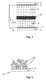
- Figure 4 shows a porous 1D PC TiO 2 electrode having multiple 1D PC TiO 2 grains 8 deposited onto a transparent conducting substrate 9 comprising a transparent conducting oxide 1 and a glass substrate 2.
- the PC grains form a network and are in physical and electrical contact with each other and the conducting substrate.
- the black lines and the spaces between the black lines represent the alternated porous layers of nanoparticles creating a periodic variation of the refractive index in the PC.
- Figure 5 shows an electrode having 1D PC grains 8 with different lattice parameters formed by the layers and having different thicknesses.
- Porous 1D PC TiO 2 grains with different lattice parameters show a difference in optical response. It is also possible to create a difference of the optical response of the 1D PC grains by varying the porosity of the alternated layers while keeping the lattice parameter constant.
- the optical response can also be changed by mixing grains containing different types of materials with different refractive index in the alternated layers.
- an electrode consisting of both porous 1D PC TiO 2 grains consisting of layers of alternated porosity of TiO 2 and porous 1D PC grains consisting of alternated layers of TiO 2 and SiO 2 can be manufactured. It is not recommended to manufacture electrodes consisting entirely of 1D PC grains that contain electrically insulating materials such as SiO 2 . However, mixtures of 1D PC grains that contain electrically insulating materials and 1D PC grains that contain semiconducting materials such as TiO 2 may be used.
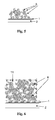
- the porous 1D PC grains 8 can be embedded in a matrix of semiconducting nanoparticles 11, see fig. 6 and fig. 7 .
- porous 1D PC grains By embedding the porous 1D PC grains in a matrix of nanoparticles with similar or the same index of refraction as the 1D PC grains, it is possible to reduce the differences in the index of refraction between the 1D PC grains and their environment. Such embedment could be used in order to reduce the light scattering effect and to reduce the opacity created by the 1D PC grains.
- 1D PC grains 8 as a diffuse scattering layer on top of a TiO 2 electrode 11.
- 1D PC grains 8 By depositing 1D PC grains on top of the TiO 2 electrode it is possible to create a diffuse light scattering layer consisting of porous 1D PC's.
- figure 9 is shown light scattering 1D PC grains 8 embedded in a matrix of TiO 2 nanoparticles 11. By embedding the 1D PC grains the light scattering effect can be reduced.
- the 1D PC grains can be produced from PC films deposited onto substrates.
- Such a PC synthesis procedure can include the following steps:
- the particles can be made of e.g., SiO 2 , TiO 2 , SnO 2 , Al 2 O 3 , MgO, ZnO, Nb 2 O 5 , CeO 2 , Fe 2 O 3 , Fe 3 O 4 , V 2 O 5 , Cr 2 O 3 , HfO 2 , MnO 2 , Mn 2 O 3 , Co 3 O 4 , NiO, Al 2 O 3 , In 2 O 3 , Sb 2 O 3 . CdS, CdSe, ZnS, ZnSe.
- the size of the nanoparticles can be in the range of 1-100 nm.
- the volume concentration of nanoparticles in the suspension can be between 0.1% and 50%.
- the nanoparticles can be produced by any technique known in the art of nanoparticle production.
- the nanoparticles can be in the form of powders or colloidal suspensions or powder suspensions.
- a suspension of nanoparticle powder can be produced using conventional techniques such as bead milling and sonication.
- the nanoparticle suspension formulation includes adequate solvents, binders or, additives etc depending on the application.
- the nanoparticle suspension formulation depends on the application at hand.
- solvents are water or alcohols etc.
- binders are PEG 20,000, PMMA, polystyrene, CarbowaxTM or ethyl cellulose, methyl cellulose etc.
- additives are dispersion additives, levelling agents, deforming agents, anti-cratering agents, waxes etc.
- PC films can be produced by depositing the nanoparticle suspensions on substrates using well known printing techniques such as: dip coating, spin coating, spraying (e.g., ultra sonic spraying), ink-jet, screen printing, rotary screen, flexo printing, gravure printing, embossed printing, Langmuir-Blodgett, slot-die coating, etc. It is preferred to use printing techniques capable of producing thin wet layers of sub-micrometer and micrometer thicknesses.
- printing techniques capable of producing thin wet layers of sub-micrometer and micrometer thicknesses.
- the multilayer structure having alternated layers can be formed by alternate deposition of layers of controlled thickness so that a periodic or quasi-periodic spatial modulation of the refractive index is attained across the multilayer.
- the solvent is allowed to evaporate.
- the deposited film can then be subjected to a brief heat treatment to assure that most of the solvent is evaporated.
- the next nanoparticle suspension layer is then printed on top of the first dried nanoparticle suspension layer and the solvent is allowed to evaporate again possibly including a heating step if necessary and so forth.
- Several additional layers can be deposited on top of each other until sufficiently many layers have been printed on top of each other to yield the desired optical properties.
- the deposited films contain organic contents, such as binder that can be dissolved during the deposition of the layers it may be necessary to ensure that the binder in the deposited dried layers is removed by combustion by heating to a higher temperature. Care must be taken that the substrate material is not destroyed at these elevated temperatures.
- the nanoparticle suspension is essentially binder free and then a lower temperature can be used.
- binders that are cross linked chemically or by heat or through light- or electron beam radiation before the application of the next layer.
- nanoparticle suspensions based on two different binders and two different solvent systems in such a way that the dissolution of the binders in the dried layers are reduced or significantly eliminated during the deposition of the layers.
- An example could be a water based nanoparticle suspension with hydroxypropyl cellulose binder and another nanoparticle suspension based on terpineol and ethyl cellulose binder. Since hydropropyl cellulose is insoluble in terpineol and since ethyl cellulose is insoluble in water it is possible to deposit alternating layers of the two different nanoparticle suspensions with reduced or eliminated dissolution of the binders in the dried layers.
- Composites of polymer with nanoparticles, exhibiting 1D photonic crystal properties, have been manufactured using UV curable polymers containing nanoparticles combined with photo initiators.
- UV curable polymer-nanoparticle systems are suitable for flexo printing purposes.
- TiO 2 based UV curable polymer nanoparticle suspensions and SiO 2 based UV curable nanoparticle suspensions can be deposited in alternated layers with a UV curing step following each layer deposition. The UV cured polymer can then be removed by combustion in to create a porous 1D PC.
- the substrate can be for example a metal foil, a polymer sheet, polymer film, or a glass substrate.
- the substrate can be a combination of the above mentioned substrates such as a polymer deposited onto a metal foil or a polymer deposited onto a glass sheet. Even a polymer deposited onto a cellulose based substrate such as paper or board can be used. It is preferred that the surface of the substrate is as smooth as possible in order to create a PC film with high optical quality.
- metal substrates could be steel foil or aluminium foil.
- polymer substrates could be PE, PP, PA, PET, PVC etc.
- the total thickness of the substrate can be around 10 micrometers or thicker.
- the deposited PC films can be removed from the substrate by for example dissolving the substrate in a solvent and then filtering the remaining PC product and then firing the filtered product.
- the PC product can be obtained directly by combusting the substrate in the case the substrate is easily combusted.
- easily combusted substrates are e.g., polymer substrates or polymer coated paper or polymer coated board.
- the PC film can also be removed by mechanical scraping in the case rigid substrates are used such as glass or steel.
- the PC can also be removed by infiltrating a polymer (5% solution of Poly(bisphenol-A-carbonate) in methylene chloride into the PC layer and then peeling off the polymer infiltrated PC layer in the form of a film.
- the self-standing polymer infiltrated film can then be heated in order to remove the polymer by combustion and in order to create mechanically stable PC grains.
- the obtained 1D PC product can be fired at some point in order to remove combustible components and to sinter the nanoparticles of each layer inside the PC grains together in order to create a mechanically stable 1D PC structure within each grain.
- the obtained 1D PC product is ground down to suitable sizes using conventional grinding equipment such as a bead mill, ball mill, or another milling technique. It is preferred that the major proportion of PC grains have sizes that are larger than the lattice spacing in the 1D PC crystal.
- Suspensions can be prepared from grinded PC grains.
- a suspension of the PC grains can be produced using conventional techniques such as stirring, bead milling and sonication techniques.
- the PC suspension formulation includes adequate solvents, binders or, additives etc depending on the application.
- the PC suspension formulation depends on the application at hand.
- solvents are water or alcohols etc.
- binders are PEG 20,000, PMMA, polystyrene, CarbowaxTM or ethyl cellulose, methyl cellulose etc.
- additives are dispersion additives, levelling agents, defoaming agents, anti-cratering agents, waxes etc.
- suspensions of PC grains with suspensions of nanoparticles and/or large non-porous light scattering particles. It is also possible to prepare suspensions containing both 1D PC grains and nanoparticles and/or large non-porous light scattering particles in one step by mixing the PC grains and nanoparticles/light scattering particles together before preparing the suspension.
- 1D PC grains can also be manufactured using template-assisted synthesis.
- An example of template-assisted synthesis is shown in the following scheme:
- the extrusion technique also allows for several layers to be extruded simultaneously thereby creating, e.g., three polymer films deposited on top of each other in on step.
- Several multilayer structures can be laminated with each other and heated in order to remove the polymer and to sinter the nanoparticles together to yield a 1D PC.
- a silica (SiO 2 ) ink consisting of 1,7% by weight of silica (surface area: 230g/m 2 ), 2.3% by weight of ethyl cellulose (viscosity 46 cP, 5 % in toluene/ethanol 80:20, Aldrich) and 96% by weight of terpineol (Fluka), was manufactured by bead milling using zirconia beads. The ink was passed through a three roll mill and finally the ink was filtered using a 1 ⁇ m PTFE filter.
- a titania ink consisting of 2.6 % by weight of titania (TiO 2 , anatase, particle size 8nm), 1.9% by weight of ethyl cellulose (viscosity 46 cP, 5 % in toluene/ethanol 80:20, Aldrich) and 95.5% by weight of terpineol was manufactured by bead milling using 0.1mm zirconia beads. The ink was passed through a three roll mill and finally the ink was filtered using a 1 ⁇ m PTFE filter.
- the titania ink and the silica ink were deposited using screen printing.
- the polyester screen used was 460 mesh.
- the printing speed was 300mm/s.
- the squeegee pressure was set to 3 bar.
- a wandress was used to remove dust from the glass substrates immediately prior to ink deposition.
- the glass substrates consisted of soda lime glass with a thickness of 2mm.
- the glass substrate area was 10cm x 10 cm.
- the printed area was 9cm x 9cm.
- First a layer of titania ink was deposited onto the glass substrate.
- the glass substrate and the deposited titania ink film was subjected to brief heat treatment (1min 180°C in air) in a conveyor belt oven to remove the solvent.
- the glass substrate and the film was subjected to heat treatment at 500°C in air for 5 minutes.
- a second layer of silica ink was deposited onto the titania layer.
- the deposited silica ink was subjected to the same thermal and cooling treatment as the titania ink.
- a multilayer consisting of alternating layers of titania /silica was manufactured by alternating deposition and thermal/cooling treatment. Alternating multi-layers consisting of 2, 4, 6, 8, 10, 12, 14, 16 layers could be manufactured this way.
- the final deposited multilayer could be removed by mechanical scraping using a doctor blade of steel, a plastic scraper or a ceramic blade such as a zirconia blade.
- the removed multilayer consisted of grains that were flat in shape and in where the grains consisted of a multilayer of alternating titania and silica, i.e., photonic crystal grains.
- the photonic crystal grains could be shaped into smaller sizes by grinding the grains using an agate mortar and a pestle.
- a silica (SiO 2 ) ink consisting of 1,7% by weight of silica (surface area: 230g/m 2 ), 10% by weight of glycerol and 88.3% by weight of terpineol (Fluka), was manufactured by bead milling using zirconia beads. The ink was passed through a three roll mill. Additionally, the ink was filtered using a 1 ⁇ m PTFE filter.
- a titania ink consisting of 2.8 % by weight of titania (TiO 2 , anatase, particle size 8nm), 10% by weight of glycerol and 87.2% by weight of terpineol was manufactured by bead milling using 0.1mm zirconia beads. The ink was passed through a three roll mill. Additionally, the ink was filtered using a 1 ⁇ m PTFE filter.
- the titania ink and the silica ink were deposited using screen printing.
- the polyester screen used was 460 mesh.
- the printing speed was 300mm/s.
- the squeegee pressure was set to 3 bar.
- a wandres was used to remove dust from the plastic substrates immediately prior to ink deposition.
- the plastic substrates consisted of polyethylene coated paper (PECP).
- the substrate area was 30cm x 30 cm.
- the printed area was 25cm x 25cm.
- First a layer of titania ink was deposited onto the PECP.
- the PECP substrate and the deposited titania ink film was subjected to brief heat treatment (10min 100°C in air) in a conveyor belt oven to remove the solvent.
- a second layer of silica ink was deposited onto the titania layer.
- the deposited silica ink was subjected to the same thermal and cooling treatment as the titania ink.
- a multilayer consisting of alternating layers of titania /silica was manufactured by alternating deposition and thermal/cooling treatment. Alternating multi-layers consisting of 2, 4, 6, 8, 10, 12, 14, 16 layers could be manufactured this way.
- the final deposited multilayer on the PECP substrate was rolled upp and put in a glass beaker and subsequently heated to 500°C for 30min in air.
- the heating caused the burning and removal of the organic PECP substrate leaving flakes of the deposited multilayer left in the glass beaker.
- the multilayer flakes were flat in shape and consisted of a multilayer of alternating titania and silica, i.e., photonic crystal grains.
- the obtained photonic crystal grains could be shaped into smaller sizes by grinding the grains using an agate mortar and a pestle.
Landscapes
- Engineering & Computer Science (AREA)
- Power Engineering (AREA)
- Microelectronics & Electronic Packaging (AREA)
- Photovoltaic Devices (AREA)
Claims (14)
- Farbstoffsolarzelle (DSC), aufweisend 1D-photonische Kristalle (PC), dadurch gekennzeichnet, dass die 1D-PC in Form von Körnern (8) vorliegen und jedes Korn (8) mehrere sich abwechselnde poröse Schichten aus halbleitenden Nanopartikeln aufweist, die eine periodische Variation eines Brechungsindex in den 1D-PC erzeugen.
- DSC nach Anspruch 1, dadurch gekennzeichnet, dass die 1D-PC-Körner unterschiedliche Porositäten und/oder Dicken und/oder Materialien der sich abwechselnden Schichten aufweisen.
- DSC nach Anspruch 1 oder 2, dadurch gekennzeichnet, dass ein großer Teil der 1D-PC-Körner Größen aufweisen, die größer sind als ein Gitterabstand in dem 1D-PC-Kristall.
- DSC nach Anspruch 1, 2 oder 3, dadurch gekennzeichnet, dass die 1D-PC-Körner eine halbleitende Elektrode des DSC bilden.
- DSC nach Anspruch 1, 2 oder 3, dadurch gekennzeichnet, dass die 1D-PC eine diffus streuende Schicht bilden.
- DSC nach Anspruch 1, 2, 3, 4 oder 5, dadurch gekennzeichnet, dass die 1D-PC-Körner aus TiO2 oder aus sich abwechselnden Schichten aus TiO2 und SiO2 bestehen.
- DSC nach Anspruch 4 oder 6, dadurch gekennzeichnet, dass die 1D-PC-Körner mit halbleitenden Elektroden-Nanopartikeln vermischt sind.
- DSC nach Anspruch 6 oder 7, dadurch gekennzeichnet, dass die 1D-PC-Körner oder die Mischung von 1D-PC-Körnern mit halbleitenden Partikeln ein Netzwerk bilden, das direkten physischen und elektrischen Kontakt zu einem leitenden Substrat der DSC hat oder indirekten Kontakt über die halbleitenden Partikel hat.
- DSC nach Anspruch 7 oder 8, dadurch gekennzeichnet, dass die halbleitenden Nanopartikel TiO2-Partikel sind.
- DSC nach einem der vorgenannten Ansprüche, dadurch gekennzeichnet, dass die 1D-PC-Körner Muster mit verschiedenen Dicken in dem DSC bilden.
- Verfahren zum Herstellen einer DSC, der einen 1D-PC aufweist, gekennzeichnet durch:- Auftragen von Nanopartikeln in Schichten auf eine Substratschicht;- Entfernen der Substratschicht; und- Zermahlen der aufgetragenen Schichtenstruktur in Körner (8);- Auftragen der Körner (8) auf die DSC durch Drucken oder Sprühen.
- Verfahren zum Herstellen einer DSC nach Anspruch 11, dadurch gekennzeichnet, dass das Auftragen der Nanopartikel durch Drucken, vorzugsweise durch Siebdruck, einer Suspension von Nanopartikeln auf das Substrat erfolgt.
- Verfahren zum Herstellen einer DSC nach Anspruch 11, dadurch gekennzeichnet, dass das Auftragen der Nanopartikel durch vorlagengestützte Synthese, Extrusion oder Schicht-auf-Schicht-Selbstmontage erfolgt.
- Verfahren zum Herstellen einer DSC nach einem der Ansprüche 11 bis 13, dadurch gekennzeichnet, dass die aufgetragene Schichtenstruktur erhitzt wird, um die Nanopartikel zu sintern.
Applications Claiming Priority (2)
| Application Number | Priority Date | Filing Date | Title |
|---|---|---|---|
| US18781609P | 2009-06-17 | 2009-06-17 | |
| PCT/EP2010/058472 WO2010146088A1 (en) | 2009-06-17 | 2010-06-16 | Dye sensitised solar cell and method of manufacture |
Publications (2)
| Publication Number | Publication Date |
|---|---|
| EP2443640A1 EP2443640A1 (de) | 2012-04-25 |
| EP2443640B1 true EP2443640B1 (de) | 2014-10-22 |
Family
ID=42358608
Family Applications (1)
| Application Number | Title | Priority Date | Filing Date |
|---|---|---|---|
| EP10726062.2A Not-in-force EP2443640B1 (de) | 2009-06-17 | 2010-06-16 | Farbstoffsensibilisierte solarzelle und verfahren zu ihrer herstellung |
Country Status (2)
| Country | Link |
|---|---|
| EP (1) | EP2443640B1 (de) |
| WO (1) | WO2010146088A1 (de) |
Cited By (2)
| Publication number | Priority date | Publication date | Assignee | Title |
|---|---|---|---|---|
| US10520923B2 (en) | 2018-05-22 | 2019-12-31 | Mantle Inc. | Method and system for automated toolpath generation |
| US10807162B2 (en) | 2016-09-15 | 2020-10-20 | Mantle Inc. | System and method for additive metal manufacturing |
Families Citing this family (3)
| Publication number | Priority date | Publication date | Assignee | Title |
|---|---|---|---|---|
| SE542946C2 (en) * | 2018-11-28 | 2020-09-22 | Stora Enso Oyj | Process for production of free standing film comprising cellulosic nanomaterial |
| KR20230092923A (ko) * | 2020-09-25 | 2023-06-26 | 레드 뱅크 테크놀로지스 엘엘씨 | 다수의 광파장을 방출하는 대역 경계 방출 강화 유기 발광 다이오드 기반 디바이스 |
| WO2026017240A1 (de) | 2024-07-16 | 2026-01-22 | Vusiongroup Gmbh | Vorrichtung zum anbringen an einem regal mit einer energy-harvesting-einrichtung |
Family Cites Families (4)
| Publication number | Priority date | Publication date | Assignee | Title |
|---|---|---|---|---|
| CH674596A5 (de) | 1988-02-12 | 1990-06-15 | Sulzer Ag | |
| ES2296533B1 (es) | 2006-09-22 | 2009-04-01 | Consejo Superior Investig. Cientificas | Procedimiento de preparacion de multicapas con estructura mesoporosa ordenada, material asi obtenido y utilizacion. |
| ES2304104B1 (es) | 2007-02-23 | 2009-08-25 | Consejo Superior De Investigaciones Cientificas | Estructura multicapa formada por laminas de nanoparticulas con propiedades de cristal fotonico unidimensional, procedimiento para su fabricacion y sus aplicaciones. |
| RU2516242C2 (ru) * | 2008-04-18 | 2014-05-20 | Нлаб Солар Аб | Устройство преобразования солнечной энергии в электрическую |
-
2010
- 2010-06-16 EP EP10726062.2A patent/EP2443640B1/de not_active Not-in-force
- 2010-06-16 WO PCT/EP2010/058472 patent/WO2010146088A1/en not_active Ceased
Cited By (8)
| Publication number | Priority date | Publication date | Assignee | Title |
|---|---|---|---|---|
| US10807162B2 (en) | 2016-09-15 | 2020-10-20 | Mantle Inc. | System and method for additive metal manufacturing |
| US11813788B2 (en) | 2016-09-15 | 2023-11-14 | Mantle Inc. | System and method for additive metal manufacturing |
| US11919224B2 (en) | 2016-09-15 | 2024-03-05 | Mantle Inc. | System and method for additive metal manufacturing |
| US10520923B2 (en) | 2018-05-22 | 2019-12-31 | Mantle Inc. | Method and system for automated toolpath generation |
| US11422532B2 (en) | 2018-05-22 | 2022-08-23 | Mantle Inc. | Method and system for automated toolpath generation |
| US11662711B2 (en) | 2018-05-22 | 2023-05-30 | Mantle Inc. | Method and system for automated toolpath generation |
| US12032356B2 (en) | 2018-05-22 | 2024-07-09 | Mantle Inc. | Method and system for automated toolpath generation |
| US12429848B2 (en) | 2018-05-22 | 2025-09-30 | Mantle Inc. | Method and system for automated toolpath generation |
Also Published As
| Publication number | Publication date |
|---|---|
| WO2010146088A1 (en) | 2010-12-23 |
| EP2443640A1 (de) | 2012-04-25 |
| HK1169885A1 (en) | 2013-02-08 |
Similar Documents
| Publication | Publication Date | Title |
|---|---|---|
| US10580588B2 (en) | Solar to electric energy conversion device | |
| Colodrero et al. | Porous one‐dimensional photonic crystals improve the power‐conversion efficiency of dye‐sensitized solar cells | |
| JP5375804B2 (ja) | 電気化学セルの製造方法 | |
| US9040816B2 (en) | Methods and apparatus for forming photovoltaic cells using electrospray | |
| US7323635B2 (en) | Photovoltaic cell | |
| EP2443640A1 (de) | Farbstoffsensibilisierte solarzelle und verfahren zu ihrer herstellung | |
| JP2002093476A (ja) | 色素増感型太陽電池セルおよびそれを用いた色素増感型太陽電池モジュール、およびそれらの製造方法 | |
| KR101172361B1 (ko) | 염료감응 태양전지용 광전극의 제조방법 | |
| JP2008258011A (ja) | 色素増感型太陽電池 | |
| US20120097243A1 (en) | Dye sensitized solar cell with improved optical characteristics | |
| JPWO2008007448A1 (ja) | 色素増感太陽電池およびそのための電極と積層フィルム | |
| HK1169885B (en) | Dye sensitised solar cell and method of manufacture | |
| WO2005074068A1 (ja) | 色素増感型太陽電池用積層フィルム ならびに色素増感型太陽電池用電極およびその製造方法 | |
| JP5021914B2 (ja) | 色素増感型太陽電池用電極 | |
| JP5209216B2 (ja) | 色素増感型太陽電池用電極およびその製造方法 | |
| JP5031997B2 (ja) | 色素増感型太陽電池用電極およびその製造方法 | |
| JP2007018951A (ja) | 色素増感型太陽電池用電極 | |
| JP4922568B2 (ja) | 色素増感型太陽電池用電極 | |
| JP5059295B2 (ja) | 色素増感型太陽電池用電極およびその製造方法 | |
| JP4922567B2 (ja) | 色素増感型太陽電池用電極 | |
| JP2011086449A (ja) | 色素増感型太陽電池用電極 | |
| JP2006252801A (ja) | 色素増感型太陽電池用電極およびその製造方法 | |
| HK1170060A (en) | Dye sensitized solar cell with improved optical characteristics | |
| HK1150188B (en) | Dye-sensitized solar cell with one-dimensional photonic crystal |
Legal Events
| Date | Code | Title | Description |
|---|---|---|---|
| PUAI | Public reference made under article 153(3) epc to a published international application that has entered the european phase |
Free format text: ORIGINAL CODE: 0009012 |
|
| 17P | Request for examination filed |
Effective date: 20111219 |
|
| AK | Designated contracting states |
Kind code of ref document: A1 Designated state(s): AL AT BE BG CH CY CZ DE DK EE ES FI FR GB GR HR HU IE IS IT LI LT LU LV MC MK MT NL NO PL PT RO SE SI SK SM TR |
|
| DAX | Request for extension of the european patent (deleted) | ||
| REG | Reference to a national code |
Ref country code: HK Ref legal event code: DE Ref document number: 1169885 Country of ref document: HK |
|
| GRAP | Despatch of communication of intention to grant a patent |
Free format text: ORIGINAL CODE: EPIDOSNIGR1 |
|
| INTG | Intention to grant announced |
Effective date: 20140526 |
|
| GRAS | Grant fee paid |
Free format text: ORIGINAL CODE: EPIDOSNIGR3 |
|
| GRAA | (expected) grant |
Free format text: ORIGINAL CODE: 0009210 |
|
| AK | Designated contracting states |
Kind code of ref document: B1 Designated state(s): AL AT BE BG CH CY CZ DE DK EE ES FI FR GB GR HR HU IE IS IT LI LT LU LV MC MK MT NL NO PL PT RO SE SI SK SM TR |
|
| REG | Reference to a national code |
Ref country code: GB Ref legal event code: FG4D |
|
| REG | Reference to a national code |
Ref country code: CH Ref legal event code: EP |
|
| REG | Reference to a national code |
Ref country code: AT Ref legal event code: REF Ref document number: 692968 Country of ref document: AT Kind code of ref document: T Effective date: 20141115 |
|
| REG | Reference to a national code |
Ref country code: IE Ref legal event code: FG4D |
|
| REG | Reference to a national code |
Ref country code: DE Ref legal event code: R096 Ref document number: 602010019685 Country of ref document: DE Effective date: 20141204 |
|
| REG | Reference to a national code |
Ref country code: SE Ref legal event code: TRGR |
|
| REG | Reference to a national code |
Ref country code: NL Ref legal event code: VDEP Effective date: 20141022 |
|
| REG | Reference to a national code |
Ref country code: AT Ref legal event code: MK05 Ref document number: 692968 Country of ref document: AT Kind code of ref document: T Effective date: 20141022 |
|
| REG | Reference to a national code |
Ref country code: LT Ref legal event code: MG4D |
|
| PG25 | Lapsed in a contracting state [announced via postgrant information from national office to epo] |
Ref country code: NL Free format text: LAPSE BECAUSE OF FAILURE TO SUBMIT A TRANSLATION OF THE DESCRIPTION OR TO PAY THE FEE WITHIN THE PRESCRIBED TIME-LIMIT Effective date: 20141022 Ref country code: ES Free format text: LAPSE BECAUSE OF FAILURE TO SUBMIT A TRANSLATION OF THE DESCRIPTION OR TO PAY THE FEE WITHIN THE PRESCRIBED TIME-LIMIT Effective date: 20141022 Ref country code: LT Free format text: LAPSE BECAUSE OF FAILURE TO SUBMIT A TRANSLATION OF THE DESCRIPTION OR TO PAY THE FEE WITHIN THE PRESCRIBED TIME-LIMIT Effective date: 20141022 Ref country code: PT Free format text: LAPSE BECAUSE OF FAILURE TO SUBMIT A TRANSLATION OF THE DESCRIPTION OR TO PAY THE FEE WITHIN THE PRESCRIBED TIME-LIMIT Effective date: 20150223 Ref country code: FI Free format text: LAPSE BECAUSE OF FAILURE TO SUBMIT A TRANSLATION OF THE DESCRIPTION OR TO PAY THE FEE WITHIN THE PRESCRIBED TIME-LIMIT Effective date: 20141022 Ref country code: IS Free format text: LAPSE BECAUSE OF FAILURE TO SUBMIT A TRANSLATION OF THE DESCRIPTION OR TO PAY THE FEE WITHIN THE PRESCRIBED TIME-LIMIT Effective date: 20150222 Ref country code: NO Free format text: LAPSE BECAUSE OF FAILURE TO SUBMIT A TRANSLATION OF THE DESCRIPTION OR TO PAY THE FEE WITHIN THE PRESCRIBED TIME-LIMIT Effective date: 20150122 |
|
| PG25 | Lapsed in a contracting state [announced via postgrant information from national office to epo] |
Ref country code: GR Free format text: LAPSE BECAUSE OF FAILURE TO SUBMIT A TRANSLATION OF THE DESCRIPTION OR TO PAY THE FEE WITHIN THE PRESCRIBED TIME-LIMIT Effective date: 20150123 Ref country code: AT Free format text: LAPSE BECAUSE OF FAILURE TO SUBMIT A TRANSLATION OF THE DESCRIPTION OR TO PAY THE FEE WITHIN THE PRESCRIBED TIME-LIMIT Effective date: 20141022 Ref country code: CY Free format text: LAPSE BECAUSE OF FAILURE TO SUBMIT A TRANSLATION OF THE DESCRIPTION OR TO PAY THE FEE WITHIN THE PRESCRIBED TIME-LIMIT Effective date: 20141022 Ref country code: HR Free format text: LAPSE BECAUSE OF FAILURE TO SUBMIT A TRANSLATION OF THE DESCRIPTION OR TO PAY THE FEE WITHIN THE PRESCRIBED TIME-LIMIT Effective date: 20141022 Ref country code: PL Free format text: LAPSE BECAUSE OF FAILURE TO SUBMIT A TRANSLATION OF THE DESCRIPTION OR TO PAY THE FEE WITHIN THE PRESCRIBED TIME-LIMIT Effective date: 20141022 Ref country code: LV Free format text: LAPSE BECAUSE OF FAILURE TO SUBMIT A TRANSLATION OF THE DESCRIPTION OR TO PAY THE FEE WITHIN THE PRESCRIBED TIME-LIMIT Effective date: 20141022 |
|
| REG | Reference to a national code |
Ref country code: DE Ref legal event code: R097 Ref document number: 602010019685 Country of ref document: DE |
|
| PG25 | Lapsed in a contracting state [announced via postgrant information from national office to epo] |
Ref country code: DK Free format text: LAPSE BECAUSE OF FAILURE TO SUBMIT A TRANSLATION OF THE DESCRIPTION OR TO PAY THE FEE WITHIN THE PRESCRIBED TIME-LIMIT Effective date: 20141022 Ref country code: EE Free format text: LAPSE BECAUSE OF FAILURE TO SUBMIT A TRANSLATION OF THE DESCRIPTION OR TO PAY THE FEE WITHIN THE PRESCRIBED TIME-LIMIT Effective date: 20141022 Ref country code: RO Free format text: LAPSE BECAUSE OF FAILURE TO SUBMIT A TRANSLATION OF THE DESCRIPTION OR TO PAY THE FEE WITHIN THE PRESCRIBED TIME-LIMIT Effective date: 20141022 Ref country code: SK Free format text: LAPSE BECAUSE OF FAILURE TO SUBMIT A TRANSLATION OF THE DESCRIPTION OR TO PAY THE FEE WITHIN THE PRESCRIBED TIME-LIMIT Effective date: 20141022 Ref country code: CZ Free format text: LAPSE BECAUSE OF FAILURE TO SUBMIT A TRANSLATION OF THE DESCRIPTION OR TO PAY THE FEE WITHIN THE PRESCRIBED TIME-LIMIT Effective date: 20141022 |
|
| PLBE | No opposition filed within time limit |
Free format text: ORIGINAL CODE: 0009261 |
|
| STAA | Information on the status of an ep patent application or granted ep patent |
Free format text: STATUS: NO OPPOSITION FILED WITHIN TIME LIMIT |
|
| REG | Reference to a national code |
Ref country code: HK Ref legal event code: GR Ref document number: 1169885 Country of ref document: HK |
|
| 26N | No opposition filed |
Effective date: 20150723 |
|
| PG25 | Lapsed in a contracting state [announced via postgrant information from national office to epo] |
Ref country code: MC Free format text: LAPSE BECAUSE OF FAILURE TO SUBMIT A TRANSLATION OF THE DESCRIPTION OR TO PAY THE FEE WITHIN THE PRESCRIBED TIME-LIMIT Effective date: 20141022 |
|
| REG | Reference to a national code |
Ref country code: CH Ref legal event code: PL |
|
| PG25 | Lapsed in a contracting state [announced via postgrant information from national office to epo] |
Ref country code: LU Free format text: LAPSE BECAUSE OF FAILURE TO SUBMIT A TRANSLATION OF THE DESCRIPTION OR TO PAY THE FEE WITHIN THE PRESCRIBED TIME-LIMIT Effective date: 20150616 Ref country code: SI Free format text: LAPSE BECAUSE OF FAILURE TO SUBMIT A TRANSLATION OF THE DESCRIPTION OR TO PAY THE FEE WITHIN THE PRESCRIBED TIME-LIMIT Effective date: 20141022 |
|
| REG | Reference to a national code |
Ref country code: IE Ref legal event code: MM4A |
|
| PG25 | Lapsed in a contracting state [announced via postgrant information from national office to epo] |
Ref country code: CH Free format text: LAPSE BECAUSE OF NON-PAYMENT OF DUE FEES Effective date: 20150630 Ref country code: LI Free format text: LAPSE BECAUSE OF NON-PAYMENT OF DUE FEES Effective date: 20150630 Ref country code: IE Free format text: LAPSE BECAUSE OF NON-PAYMENT OF DUE FEES Effective date: 20150616 |
|
| REG | Reference to a national code |
Ref country code: FR Ref legal event code: PLFP Year of fee payment: 7 |
|
| PG25 | Lapsed in a contracting state [announced via postgrant information from national office to epo] |
Ref country code: MT Free format text: LAPSE BECAUSE OF FAILURE TO SUBMIT A TRANSLATION OF THE DESCRIPTION OR TO PAY THE FEE WITHIN THE PRESCRIBED TIME-LIMIT Effective date: 20141022 |
|
| PG25 | Lapsed in a contracting state [announced via postgrant information from national office to epo] |
Ref country code: BG Free format text: LAPSE BECAUSE OF FAILURE TO SUBMIT A TRANSLATION OF THE DESCRIPTION OR TO PAY THE FEE WITHIN THE PRESCRIBED TIME-LIMIT Effective date: 20141022 Ref country code: HU Free format text: LAPSE BECAUSE OF FAILURE TO SUBMIT A TRANSLATION OF THE DESCRIPTION OR TO PAY THE FEE WITHIN THE PRESCRIBED TIME-LIMIT; INVALID AB INITIO Effective date: 20100616 Ref country code: SM Free format text: LAPSE BECAUSE OF FAILURE TO SUBMIT A TRANSLATION OF THE DESCRIPTION OR TO PAY THE FEE WITHIN THE PRESCRIBED TIME-LIMIT Effective date: 20141022 |
|
| REG | Reference to a national code |
Ref country code: FR Ref legal event code: PLFP Year of fee payment: 8 |
|
| PG25 | Lapsed in a contracting state [announced via postgrant information from national office to epo] |
Ref country code: TR Free format text: LAPSE BECAUSE OF FAILURE TO SUBMIT A TRANSLATION OF THE DESCRIPTION OR TO PAY THE FEE WITHIN THE PRESCRIBED TIME-LIMIT Effective date: 20141022 |
|
| PG25 | Lapsed in a contracting state [announced via postgrant information from national office to epo] |
Ref country code: BE Free format text: LAPSE BECAUSE OF FAILURE TO SUBMIT A TRANSLATION OF THE DESCRIPTION OR TO PAY THE FEE WITHIN THE PRESCRIBED TIME-LIMIT Effective date: 20141022 |
|
| REG | Reference to a national code |
Ref country code: FR Ref legal event code: PLFP Year of fee payment: 9 |
|
| PG25 | Lapsed in a contracting state [announced via postgrant information from national office to epo] |
Ref country code: MK Free format text: LAPSE BECAUSE OF FAILURE TO SUBMIT A TRANSLATION OF THE DESCRIPTION OR TO PAY THE FEE WITHIN THE PRESCRIBED TIME-LIMIT Effective date: 20141022 |
|
| PG25 | Lapsed in a contracting state [announced via postgrant information from national office to epo] |
Ref country code: AL Free format text: LAPSE BECAUSE OF FAILURE TO SUBMIT A TRANSLATION OF THE DESCRIPTION OR TO PAY THE FEE WITHIN THE PRESCRIBED TIME-LIMIT Effective date: 20141022 |
|
| PGFP | Annual fee paid to national office [announced via postgrant information from national office to epo] |
Ref country code: IT Payment date: 20190607 Year of fee payment: 10 |
|
| PGFP | Annual fee paid to national office [announced via postgrant information from national office to epo] |
Ref country code: SE Payment date: 20190627 Year of fee payment: 10 Ref country code: FR Payment date: 20190625 Year of fee payment: 10 |
|
| PGFP | Annual fee paid to national office [announced via postgrant information from national office to epo] |
Ref country code: GB Payment date: 20190627 Year of fee payment: 10 Ref country code: DE Payment date: 20190627 Year of fee payment: 10 |
|
| REG | Reference to a national code |
Ref country code: DE Ref legal event code: R119 Ref document number: 602010019685 Country of ref document: DE |
|
| GBPC | Gb: european patent ceased through non-payment of renewal fee |
Effective date: 20200616 |
|
| PG25 | Lapsed in a contracting state [announced via postgrant information from national office to epo] |
Ref country code: FR Free format text: LAPSE BECAUSE OF NON-PAYMENT OF DUE FEES Effective date: 20200630 Ref country code: GB Free format text: LAPSE BECAUSE OF NON-PAYMENT OF DUE FEES Effective date: 20200616 |
|
| PG25 | Lapsed in a contracting state [announced via postgrant information from national office to epo] |
Ref country code: DE Free format text: LAPSE BECAUSE OF NON-PAYMENT OF DUE FEES Effective date: 20210101 Ref country code: SE Free format text: LAPSE BECAUSE OF NON-PAYMENT OF DUE FEES Effective date: 20200617 |
|
| REG | Reference to a national code |
Ref country code: SE Ref legal event code: EUG |
|
| PG25 | Lapsed in a contracting state [announced via postgrant information from national office to epo] |
Ref country code: IT Free format text: LAPSE BECAUSE OF NON-PAYMENT OF DUE FEES Effective date: 20200616 |