EP2446532B1 - Filterkreis - Google Patents
Filterkreis Download PDFInfo
- Publication number
- EP2446532B1 EP2446532B1 EP09785970.6A EP09785970A EP2446532B1 EP 2446532 B1 EP2446532 B1 EP 2446532B1 EP 09785970 A EP09785970 A EP 09785970A EP 2446532 B1 EP2446532 B1 EP 2446532B1
- Authority
- EP
- European Patent Office
- Prior art keywords
- amplifier
- resonator
- output port
- filter
- resonators
- Prior art date
- Legal status (The legal status is an assumption and is not a legal conclusion. Google has not performed a legal analysis and makes no representation as to the accuracy of the status listed.)
- Not-in-force
Links
- 238000000034 method Methods 0.000 claims description 35
- 230000005540 biological transmission Effects 0.000 claims description 34
- 230000004044 response Effects 0.000 claims description 29
- 238000012546 transfer Methods 0.000 claims description 14
- 238000001914 filtration Methods 0.000 claims description 10
- 230000003139 buffering effect Effects 0.000 claims description 9
- 239000003990 capacitor Substances 0.000 description 65
- 238000010586 diagram Methods 0.000 description 16
- 238000013461 design Methods 0.000 description 12
- 230000000694 effects Effects 0.000 description 12
- 230000004048 modification Effects 0.000 description 7
- 238000012986 modification Methods 0.000 description 7
- 230000008859 change Effects 0.000 description 6
- 238000010897 surface acoustic wave method Methods 0.000 description 6
- 238000004458 analytical method Methods 0.000 description 5
- 238000004519 manufacturing process Methods 0.000 description 5
- 230000008569 process Effects 0.000 description 4
- 230000003321 amplification Effects 0.000 description 3
- 239000000919 ceramic Substances 0.000 description 3
- 230000003247 decreasing effect Effects 0.000 description 3
- 239000010408 film Substances 0.000 description 3
- 239000000463 material Substances 0.000 description 3
- 238000003199 nucleic acid amplification method Methods 0.000 description 3
- 230000007704 transition Effects 0.000 description 3
- 230000000903 blocking effect Effects 0.000 description 2
- 239000013078 crystal Substances 0.000 description 2
- 230000001747 exhibiting effect Effects 0.000 description 2
- 239000010409 thin film Substances 0.000 description 2
- 229910003327 LiNbO3 Inorganic materials 0.000 description 1
- XUIMIQQOPSSXEZ-UHFFFAOYSA-N Silicon Chemical compound [Si] XUIMIQQOPSSXEZ-UHFFFAOYSA-N 0.000 description 1
- 230000002238 attenuated effect Effects 0.000 description 1
- 239000000872 buffer Substances 0.000 description 1
- 238000010276 construction Methods 0.000 description 1
- 230000008878 coupling Effects 0.000 description 1
- 238000010168 coupling process Methods 0.000 description 1
- 238000005859 coupling reaction Methods 0.000 description 1
- 230000007812 deficiency Effects 0.000 description 1
- 230000006866 deterioration Effects 0.000 description 1
- 238000005516 engineering process Methods 0.000 description 1
- 230000005669 field effect Effects 0.000 description 1
- 230000003993 interaction Effects 0.000 description 1
- GQYHUHYESMUTHG-UHFFFAOYSA-N lithium niobate Chemical compound [Li+].[O-][Nb](=O)=O GQYHUHYESMUTHG-UHFFFAOYSA-N 0.000 description 1
- 230000007246 mechanism Effects 0.000 description 1
- 230000007935 neutral effect Effects 0.000 description 1
- 238000012545 processing Methods 0.000 description 1
- 239000010453 quartz Substances 0.000 description 1
- 230000035945 sensitivity Effects 0.000 description 1
- 238000007493 shaping process Methods 0.000 description 1
- 229910052710 silicon Inorganic materials 0.000 description 1
- 239000010703 silicon Substances 0.000 description 1
- VYPSYNLAJGMNEJ-UHFFFAOYSA-N silicon dioxide Inorganic materials O=[Si]=O VYPSYNLAJGMNEJ-UHFFFAOYSA-N 0.000 description 1
- 230000001629 suppression Effects 0.000 description 1
Images





Classifications
-
- H—ELECTRICITY
- H03—ELECTRONIC CIRCUITRY
- H03H—IMPEDANCE NETWORKS, e.g. RESONANT CIRCUITS; RESONATORS
- H03H9/00—Networks comprising electromechanical or electro-acoustic elements; Electromechanical resonators
- H03H9/46—Filters
- H03H9/54—Filters comprising resonators of piezoelectric or electrostrictive material
- H03H9/545—Filters comprising resonators of piezoelectric or electrostrictive material including active elements
-
- H—ELECTRICITY
- H03—ELECTRONIC CIRCUITRY
- H03H—IMPEDANCE NETWORKS, e.g. RESONANT CIRCUITS; RESONATORS
- H03H11/00—Networks using active elements
- H03H11/02—Multiple-port networks
- H03H11/04—Frequency selective two-port networks
-
- H—ELECTRICITY
- H03—ELECTRONIC CIRCUITRY
- H03H—IMPEDANCE NETWORKS, e.g. RESONANT CIRCUITS; RESONATORS
- H03H11/00—Networks using active elements
- H03H11/02—Multiple-port networks
- H03H11/04—Frequency selective two-port networks
- H03H11/12—Frequency selective two-port networks using amplifiers with feedback
- H03H11/1208—Frequency selective two-port networks using amplifiers with feedback comprising an electromechanical resonator
Definitions
- This invention concerns a filter circuit for processing analog signals, and more specifically an active electronic filter combining buffering devices with resonators.
- IF filters in radio frequencies have been realized as surface-acoustic wave (SAW) filters or as ceramic filters.
- SAW surface-acoustic wave
- the electric signal is converted to a mechanical wave that propagates in some mechanical resonator.
- the mechanical resonance frequency is the same as the frequency of the electrical signal, the signal is amplified; otherwise, it is suppressed.
- the filter transfer characteristics are defined by the mechanical parameters of the resonator: its size, material, the mode of the mechanical wave in the resonator, etc.
- SAW filters the waves travel on the surface of some piezoelectric material like Lithium Niobate (LiNbO 3 ), while in ceramic filters, piezoceramic is used as the resonator.
- SAW filters have been replaced by Film Bulk Acoustic Resonator (FBAR) filters. Similar to SAW filters, FBAR filters also employ mechanical resonance to achieve stable narrowband frequency response with sharp cut-offs.
- the mechanical resonator is a thin film layer, and the mechanical wave propagates in the bulk of the layer. Filters based on FBARs have several advantages over SAW and ceramic filters, including better temperature stability, smaller size, compatibility with existing silicon technology, higher operating frequency range, ability to handle higher power, better electrostatic discharge sensitivity, and higher quality factor (Q-factor).
- An FBAR exhibits two resonance values: one series, f s , and one parallel, f p .
- Behavior of an FBAR resonator across a range of frequencies is illustrated in Figure 1c , which shows the reactance of the resonator vs. frequency.
- the reactance is 0; the resonator acts like a short circuit; and a signal passes freely through the resonator.
- the reactance goes to infinity; the resonator acts like an open circuit; and a signal is blocked by the resonator.
- the resistances in the MBVD equivalent circuit are very small compared with the impedance of the other circuit elements, and they are often neglected in theoretical analyses.
- the relative distance between series and parallel resonance frequencies f s and f p is about 2-3% and the Q-factor of an FBAR varies between 300 and 2500.
- FBAR filters Two basic structures are commonly used for creating FBAR filters: ladder and lattice.
- a ladder filter structure a number of resonators are connected in series, with a shunt resonator connected to ground between each two adjacent series resonators.
- the central passband frequency of the ladder FBAR filter is defined by the series resonance frequency f s ,series of the series resonators and the parallel resonance frequency f p, shunt of the shunt resonators, which are all equal.
- the series resonators are equivalent to short circuits at this frequency, connecting the filter input directly with the filter output.
- the shunt resonators are equivalent to open circuits at the same frequency and have no effect.
- the gain of the circuit is equal to one, which is the maximum gain of the filter. The gain in a small vicinity around this frequency is close to 1, which forms the filter passband.
- Ladder FBAR filters present several disadvantages. First, they require many resonators in order to achieve reasonable attenuation in the stopband. In addition, constraints on the parameters of the resonators often necessitate adding additional elements such as inductors and capacitors in order to properly adjust the resonance frequencies of each FBAR in the filter. A third disadvantage is that adjustment of the filter characteristics with capacitors and inductors is often inconvenient and complicated. Finally, ladder filters do not allow significant extension of the filter passband bandwidth. The passband bandwidth is limited by the series resonance of the shunt FBARs and by the parallel resonance of the series FBARs.
- a lattice filter circuit using resonators is shown in Figure 1a .
- a lattice filter circuit, or bridge circuit employs two different pairs of identical resonators.
- the parallel resonance frequency of one pair of resonators, 130 and 140 must equal the series resonance frequency of the other pair of resonators, 150 and 160.
- the passband theoretically extends from the series resonance frequency of the 130-140 pair to the parallel resonance frequency of the 150-160 pair. (In practice, the passband in the real circuit is slightly narrower within that range.)
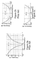
- Figure 2a is a graphical representation of the attenuation of a signal in a lattice filter as a function of signal frequency.
- Figure 2b is a more detailed representation of attenuation vs. frequency within the passband. As can be seen in the graphs, signal attenuation of the lattice filter increases monotonically in the stopband. In the ladder filter, in contrast, signal attenuation peaks at the edge of the passband and then returns rapidly to very low values.
- resonators 130 and 140 are in parallel resonance, and resonators 150 and 160 are in series resonance.
- resonators 130 and 140 act as open circuits, and resonators 150 and 160 act as short circuits, and the filter input is directly connected to the filter output, producing a maximum signal.
- the resonator characteristics that determine the resonant frequencies thereby determine the first frequency f 0 .
- the second frequency of minimum attenuation occurs because, neglecting power losses in the resonators, the complex impedances Z a of resonator pair 130-140 and Z b of resonator pair 150-160 may be considered purely imaginary, as noted earlier.
- the imaginary component of the impedance values (reactance) of a resonator as a function of frequency is shown in the graph of Figure 1c . Inside the frequency band f sa ⁇ f ⁇ f pb , the impedances of resonator pairs 130-140 and 150-160 have opposite signs, and their product Z a Z b is thus real and positive within this frequency band.
- the value of the product Z a Z b increases monotonically from 0 to infinity in the interval f sa ⁇ f ⁇ f pb .
- Figure 2c is a graphical representation of the attenuation vs. frequency within the passband of a lattice filter at a particular resistance value, showing two different attenuation minima in the passband.
- the resistances affecting attenuation in a lattice filter include resistance values external to the filter circuit, i.e., the source and load resistances 120 and 180 in Figure 1a . These resistances are exterior to the input terminals 112 and 114, and the output terminals 176 and 178, respectively. As such, their values are not necessarily accessible for adjustment in most applications.
- filter response may also be shaped by creating transmission zeros, or frequencies at which input signals are completely blocked by the system.
- the monotonically increasing frequency response of the lattice filter in the stopbands is due to the lack of transmission zeros in its transfer function.
- the existence of transmission zeros depends on the parameters of the resonators used in the circuit; and, if necessary, transmission zeros can be created by an appropriate design of the filter.
- a lattice filter based on piezoelectric resonators can have two transmission zeros - one below the passband and another above the passband.
- the input impedance of the filter does not change significantly for the other passband frequencies, and the cascade connection of several lattice stages does not significantly increase the maximum passband attenuation.
- a significant disadvantage of FBAR lattice filters is the large number of resonators, a minimum of four for a single stage lattice filter.
- each pair of resonators must have identical operating parameters.
- tuning elements of a lattice filter that are parts of the filter circuit must also have identical operating parameters.
- the use of tuning elements outside of the lattice, suggested in some prior art, results in the tuning elements being applied to all resonators in the lattice and simultaneously changing the resonance frequencies of all resonators.
- Transmission zeros (attenuation poles) are created in lattice filters by proper choice of the parameters of the resonators, effectively, choice of the values of the elements of their equivalent circuits.
- elements added to tune the filter passband alter the equivalent circuit of the combination of the FBAR and the tuning elements, affecting the position of the transmission zeros.
- designing thin film resonators to conform to application-related specifications is driven by requirements for precise control of the resonance frequencies, optimal connections, maximum Q-factors, and purity of the main resonance.
- the resonance frequency is affected by both the resonator and the electrode thicknesses, necessitating precise control over the thickness and properties of the layers during manufacture.
- the design of the electrodes further represents trade-offs between low sheet resistivity, efficient electromechanical coupling, and high acoustic quality of the materials used.
- Limitations in manufacturing processes dictate the necessity of tuning the filters post-manufacture to conform to operating specifications.
- the tuning of resonance frequencies of identical resonators in conventional lattice filters is a complex procedure because the additional circuit elements must be matched and because other interactions of circuit elements are affected by the tuning process.
- a filter circuit comprises a first amplifier that receives an input signal at an input port and generates a differential output signal at a positive output port and a negative output port.
- the circuit further comprises a first resonator having a series and a parallel resonant frequency connected to the positive output port of the first amplifier and a second resonator with a series and a parallel resonant frequency connected to the negative output port of the first amplifier.
- the outputs of the first and second resonators are electrically coupled to one another and further connected to an input port of a second amplification device, which receives the output of the first and second resonators and outputs a filtered signal.
- the first resonator and second resonator may have third order or higher impedances.
- the series resonant frequency of one of the resonators is substantially equal to the parallel resonant frequency of the other resonator.
- the first resonator and second resonator may be film bulk acoustic resonators (FBARs), and the series and parallel resonant frequencies of the first and second resonators may be selected so that the first and second resonators pass a desired frequency range of the input signal.
- the first amplifier may have sufficiently high input and output impedances to minimize the effects on the input signal from resistances external to the filter circuit.
- the first amplifier may be an Operational Transconductance Amplifier (OTA), and may have adjustable gain.
- OTA Operational Transconductance Amplifier
- the second amplifier may be a transresistance amplifier or a current amplifier.
- At least one resistor possibly a variable resistor, may be connected in series or in parallel to at least one of the output ports of the first amplifier.
- At least one capacitor possibly a variable capacitor, may be connected in series or in parallel with at least one of the resonators.
- At least one inductor may be connected in series or in parallel with at least one of the resonators.
- At least one additional resonator which may be an FBAR, may be connected in series or in parallel to at least one of the first and second resonators.
- a method of filtering signals includes the activities of receiving a signal from a signal source and generating a differential output signal from the received signal at the positive output port and negative output port of a first amplifier.
- the differential ouput signal is passed through a first resonator connected to a positive output port of the first amplifier and a resistance at the positive output port of the first amplifier.
- the differential output signal is passed through a second resonator connected to a negative output port of the first amplifier and a resistance at the negative output port of the first amplifier.
- the outputs of the first resonator and the second resonator are electrically coupled to produce a combined signal.
- the combined signal is passed through a buffering device to generate a filtered output signal. Passing the combined signal through the second amplification device may minimize the effects on the combined signal from an external load.
- the method of filtering signals may further comprise adjusting internal resistances of the filter circuit to achieve a desired frequency passband.
- the adjustment may apply a bias voltage to the first amplifier, or pass the positive differential signal or the negative differential signal through at least one resistor in series or in parallel with at least one of the output ports of first amplifier.
- the resistors may be variable resistors.
- the differential output signal may be passed through at least one capacitor or inductor, connected in series or in parallel with at least one of the first resonator and second resonator of the filter circuit to achieve a desired filter passband.
- the differential output signal may be passed through at least one additional resonator, connected in series or in parallel with at least one of the first resonator and second resonator of the filter circuit to achieve a desired filter passband.
- the method of filtering signals may further comprise adjusting the internal resistance to comprise two differing resistances, either by providing a first resistance at the positive output port of the first amplifier, and a different, second resistance at the negative output port of the first amplifier or by selecting or adjusting the first amplifier to have differing internal resistances at its positive output port and its negative output port to create transmission zeros in the filter transfer function.
- the resistance values of the two differing resistances may be adjusted to vary values of the transmission zeros in the filter transfer function.
- the filter circuit described herein contains only half the number of resonators of a conventional lattice filter.
- the circuit avoids the requirement in conventional lattice filters of matched pairs of identical resonators.
- Tuning of the resonance frequencies of the resonators in the filter circuit may be accomplished by using extra capacitors or inductors, the effects of which are separate and independent for each resonator.
- the amplifiers at the input and output of the filter further permit implementation of a variable gain within the filter passband. They also separate input and output impedances, allowing operation with different source and load resistances.
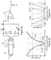
- Figure 3a is a circuit diagram of a filter according to principles of the present invention.
- An input signal ( V in ) is received from a signal source 310.
- An arbitrary resistance 320 represents the load of the circuit external to the filter input.
- the filter circuit may have an input amplifier 330, an output amplifier 370, and first and second resonators, 340 and 350 connected therebetween.
- Input amplifier 330 may have differential input ports 332 and 333, receiving a balanced input signal from the signal source 310.
- the input of input amplifier 330 may be differential or single-ended, depending on other constraints of the filter implementation.
- Input amplifier 330 has differential output ports, 335 and 336.
- input amplifier 330 is illustrated as an Operational Transconductance Amplifier (OTA), often used for signals in the GHz range.
- An additional terminal 338 shown connected to ground may be a middle, neutral point of the output. It can be either a dc biasing terminal or an intentionally added terminal of the amplifier.
- input amplifier 330 may be any amplifier having characteristics able to separate the signal source from the filter, and output the signal to be amplified as paired differential values.
- the input amplifier 330 has input and output impedance characteristics selected to reduce the effects of the internal impedance of the signal source on the filter frequency response.
- Input amplifier 330 converts a voltage at its input ports ( V in ) to a differential current (voltage-to-current converter) at its output ports.
- Input amplifier 330 is characterized by the values of its transconductance (amplifier output current versus amplifier input voltage) and its input and output impedances. Input amplifier 330 may alternatively be realized as any other kind of amplifier operating in the expected signal frequency range, providing a differential output, and able to prevent the signal source internal impedance from affecting the filter parameters.
- a first resonator 340 may be connected to a positive output port 335 of input amplifier 330.
- the first resonator 340 has two resonant frequencies, f as (series resonant frequency) and f ap (parallel resonant frequency).
- the resonant frequencies normally differ by about 2%-3% if FBAR resonators are used. However, the difference between the resonant frequencies may be smaller or larger. Recalling the behavior shown in Figure 1c , for signals near its parallel resonant frequency, the reactance in the resonator is high; and first resonator 340 acts as an open circuit, blocking the signals.
- resonator 340 is a Film Bulk Acoustic Resonator (an FBAR), and its first electrode is connected to the positive output port 335 of input amplifier 330.
- FBAR Film Bulk Acoustic Resonator
- MMVD Butterworth-Van Dyke
- the second resonator 350 may be connected to a negative output port 336 of input amplifier 330.
- the second resonator 350 has two resonant frequencies, f bs (series resonant frequency) and f bp (parallel resonant frequency).
- the resonant frequencies normally differ by about 2%-3% if FBAR resonators are used. However, the difference may be smaller or larger.
- the reactance increases; and second resonator 350 acts as an open circuit, blocking the signals.
- the second resonator 350 acts as a short circuit, passing the signals therethrough.
- second resonator 350 is an FBAR, and its first electrode is connected to the negative output port 336 of input amplifier 330.
- Different resonators such as quartz-crystal resonators, mechanical resonators, or other types, may be appropriately substituted, especially for different operational frequency ranges.
- any resonator able to accomplish the above filtering having a similar equivalent MBVD circuit may be used.
- a single continuous passband of signal frequencies is created, approximately from f as to f bp .
- the outputs of the first and second resonators are coupled together at an input port 372 of output amplifier 370, providing an input signal of frequency range substantially between f as and f bp to output amplifier 370.
- other types of resonators or circuit elements exhibiting the characteristics required to accomplish this filtering may be substituted for the FBARs illustrated in Figure 3a , including but not limited to quartz crystals, piezoceramic resonators, or ferroelectric resonators.
- Output amplifier 370 has a very small input impedance (0 in the ideal case).
- the input port 372 of output amplifier 370 may be single-ended, while its output may be either single-ended or differential, depending on the filter implementation. (In the example, the negative input port 373 is shown connected to ground.)
- the very small input impedance allows summing of the currents through the resonators 340 and 350 without affecting the values of these currents.
- the output amplifier produces a signal (output voltage or output current), which is proportional to the sum of the currents through the resonators.
- output amplifier 370 is shown as a transresistance amplifier (output voltage vs. input current), producing a voltage signal at its output port 375.
- Output amplifier 370 may alternatively be a current amplifier (output current vs. input current), such as a common-base amplifier (with bipolar transistors) or common-gate amplifier (with field-effect transistors), or any other amplifier able to separate the load from the filter, avoiding the influence of the load impedance on the filter frequency response and produce an output signal proportional to the sum of the currents through the first resonator and second resonator.
- the circuit load external to the output port of output amplifier 370 is shown for purposes of example as a single resistance 380.
- Resistors 392 and 394 are drawn in dashed lines in parallel across the two arms of the circuit. Resistors 392 and 394 represent either the output resistances of both halves of input amplifier 330, or a combination of those values with additionally added resistors as discussed further below. The resistors are representative of inherent resistances within the filter circuit and are not necessarily present as elements of the circuit.
- Equations (1) and (3) indicate that the attenuation of the signal passing through the filter circuit should be similar to the attenuation of the signal passing through a conventional lattice filter, i.e., the frequency behavior should be similar to that of a lattice filter. This similar behavior may be seen in the solid line of attenuation vs. frequency in the graphs of Figures 3b and 3c .
- the only difference in the equations is the presence of the factor g m 1 r m 2 in the numerator of equation (3). This factor reflects the gain of the amplifiers, and its presence indicates that the filter circuit in Figure 3a also allows for arbitrary amplification of the signal.
- the filter circuit of Figure 3a has the properties of the lattice filter, although it includes only two resonators.
- the requirement that f ap f bs also holds for this filter circuit.
- it is a less stringent constraint, since it applies only to single resonators rather than being a requirement for each of the matched resonator pairs as in a conventional lattice filter.
- Figures 3b and 3c illustrate the behavior of the circuit with regard to signal attenuation.
- Figure 3b shows the signal attenuation across the normalized frequency range
- Figure 3c is a more detailed representation of signal attenuation within the passband.
- the filter circuit exhibits good signal selectivity, with narrow roll-off.
- the circuit also allows an adjustable gain in the passband, achieved by varying the gain of the amplifiers.
- R represents only the resistance internal to the filter, since amplifiers 330 and 370 prevent the external source and load impedances from affecting the filter frequency response. Changing this resistance causes a corresponding adjustment of the passband, as seen in Figures 3b and 3c (dashed line and dotted line).
- Figures 3b and 3c are graphical representations of a frequency response of the filter in Figure3a with a normalized frequency, for different values of the resistance R .
- f sa 0.975
- Figure 3b shows the overall frequency response
- Figure 3c shows the passband frequency response in greater detail.
- increasing the internal resistance moves the passband to a higher frequency range
- decreasing the internal resistance moves the passband to a lower frequency range.
- the filter circuit advantageously provides a straightforward tuning mechanism for adjusting the filter passband.
- the amplifiers 330 and 370 in Figure 3a act to isolate the filter from the loads on the circuit, serving as buffers from the remainder of the circuit external to the filter and permitting differing terminating resistances 320 and 380 at both sides of the filter. Because the influence of the load resistances on the filter frequency response is avoided, the load resistances can be arbitrary.
- the resistances 392 or 394 R in formula (1) are completely internal to the circuit. Since the values of these resistances are not affected by the outer circuitry, using them for tuning the filter passband is a straightforward procedure.
- the tuning range achieved by varying the resistors is limited by the frequencies f sa and f pb , and by the hump in the frequency response that appears between the two frequencies of minimum attenuation when the resistance R differs from the value of R 0 for frequency f 0 (best seen in Figure 3c ).
- the tuning range of resistance adjustment is approximately the same as for FBAR lattice filters tuned by adding additional capacitors.
- Adjusting the passband of the filter by varying resistors 392 and 394 has several advantages in actual practice.
- resistors usually consume less chip area than inductors and capacitors.
- the resistors 392 and 394 can be part of input amplifier 330, i.e., they need not even exist as separate elements in the physical circuit.
- capacitors and inductors added in parallel or in series to the resonators decrease the Q -factors of the resonators, adjusting the resistances does not affect the resonator Q -factor.
- the passband bandwidth is narrowed by varying the resistor values, the effect is much less than if capacitors are added to the circuit.
- tuning the passband by adjusting resistor values does not preclude adjusting the resonator frequencies with extra inductors and capacitors. The combination of both tuning methods permits more flexibility in design and operation.
- Variation of the values of the resistors 392 and 394 can be accomplished in several ways.
- the output resistance of input amplifier 330 may be tuned by changing the DC quiescent point of its output stage (biasing the amplifier).
- variable resistors can be added in parallel or in series to the outputs of input amplifier 330. These resistors can be tuned electronically by DC voltage or current.
- the resistances may also be provided by resistor banks, consisting of a plurality of resistors and electronic switches for selecting to include them into the filter circuit. Any alternative technique or combination of techniques may be used that adjusts the value of the internal resistance in the filter circuit, to accomplish tuning of the passband frequency.
- Figure 4a shows a simplified model of the filter circuit. Circuit elements corresponding to elements in Figure 3a are identified with similar reference numbers.
- the current through the grounded terminal 338 is substantially 0, as shown in Figure 4a .
- Resistors 392 and 394 are shown outside of first amplifier 330. These resistors could be part of the first amplifier (the output resistances of this amplifier). Alternatively, the resistors 392 and 394 may be a combination of the amplifier output resistances and externally added resistors. To simplify the analysis, first amplifier 330 is considered as an ideal transconductance amplifier with infinite output impedance, and its output resistances 392 and 394 are considered as externally added in parallel to the outputs 335 and 336.
- the second amplifier 370 may have zero input impedance. Its input current I i 2 is taken from the point 360 between the two resonators 340 and 350. This current returns at the point 390 between resistors 392 and 394 after passing through the input of the second amplifier 370 and through ground. Thus, resistors 392 and 394 and resonators 340 and 350 form a bridge circuit, and the current I i 2 is the imbalance current of the bridge.
- the filtering properties are defined by the relationship between the currents I o1 and I i 2 , since I o 1 is proportional to the filter input voltage or input current; and I i 2 is proportional to the filter output voltage or output current.
- the sum of the currents I Ra through resistor 392 and I Qa through first resonator 340 may be substantially equal to I o 1 .
- the voltages over these two elements may be substantially equal, since the voltage drop over the input of second amplifier 370 may be substantially 0.
- Resonator 340 behaves like a reactive element: as an inductor between f sa and f pa , and as a capacitor at other frequencies.
- the current through resistor 392 is V / R a , where V is the voltage over the resistor and R a is its resistance.
- the current through resonator 340 is V /( j 2 ⁇ fL eq ) when the resonator behaves like an inductor ( L eq is the equivalent inductance).
- the current is V ⁇ ( j 2 ⁇ fC eq ) when the resonator behaves like a capacitor ( C eq is the equivalent capacitance).
- C eq is the equivalent capacitance
- resistor 394 and resonator 350 Similar analysis and similar conclusions hold for resistor 394 and resonator 350: the current I Qb through resonator 350 is shifted by 90° behind the current I Rb when the resonator is equivalent to an inductor, and is shifted by 90° ahead of I Rb when the resonator acts as a capacitor.
- Resonators 340 and 350 have opposite behavior within the passband.
- resonator 340 is equivalent to an inductor, while resonator 350 behaves like a capacitor in the same frequency range.
- f sb f pa ⁇ f ⁇ f pb , their characteristics are interchanged: resonator 350 is equivalent to an inductor, while resonator 340 is equivalent to a capacitor.
- Figure 4b shows the relationship of the phasors of the currents through the two resonators (representing the amplitudes and phases of the currents) in the frequency band f sa ⁇ f ⁇ f pb .
- the currents I Ra through resistor 392 and I Qa through resonator 340 are in quadrature, and their sum is equal to I o 1 .
- the phasors I o 1 , I Qa and I Ra form a right triangle. If they are plotted as shown in Figure 4b , the end of I Qa moves along the lower semicircle as the frequency varies from f sa to f pa .
- the currents I Qb and I Rb are also in quadrature; and their sum is equal to I o 1 .
- the end of I Qb moves along the upper semicircle in Figure 4b .
- the endpoint of I Qb moves toward point A.
- resonator 350 Since resonator 350 has series resonance at this frequency, it is equivalent to a short circuit; and the entire current I o 1 flows through resonator 350.
- I i 2 I Qa ⁇ I Qb .
- the phasor I i2 representing the input current of amplifier 370, connects the ends of phasors I Qa and I Qb . These ends are at opposite sides of the circle of diameter I o 1 , and the length of I i 2 is relatively large, corresponding to the large gain of the filter inside the passband.
- the filter has maximum gain at these two frequencies.
- both the resonators behave like capacitors. They have values close to their equivalent capacitances, which define approximately equal phasors I Qa and I Qb .
- Figure 4c shows the phasors of the currents in this case. The ends of the phasors I Qa and I Qb are close to each other, and the distance between their ends is small, which explains the small filter gain in the stopband.
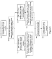
- An exemplary method of filtering signals using the circuit of Figure 3 a is shown in the flow diagram of Figure 6 .
- An input signal may be received at an input port of an input amplifier 330 as discussed in step 610.
- a balanced input signal may be received at both input ports 332 and 333 of an input amplifier 330 that accepts balanced input signals.
- the input amplifier 330 separates the signal from the internal impedance 320 of the signal source as stated in step 620, so that filter operating parameters are not significantly affected by the signal source internal impedance.
- Differential output signals (voltage or current) may be generated by input amplifier 330 at positive 335 and negative 336 output ports.
- input amplifier 330 converts the input signals to substantially equal currents at output ports 335 and 336, and the remainder of the filtering method uses terminology based on currents.
- the input amplifier may convert the input signal to equal voltages, and the resistors 392 and 394 may be in series with these voltages and resonators 340 and 350 respectively.
- the current from the positive output port 335 of input amplifier 330 is split between the first electrode of a first resonator 340 and resistor 392 as described in step 630.
- the frequency f of the current passing through the first resonator is less than its series resonant frequency ( f sa ⁇ f )
- the resonator acts like a capacitor.
- the frequency f of the current passing through first resonator 340 is between its series resonant frequency and its parallel resonant frequency ( f sa ⁇ f ⁇ f pa )
- the resonator acts like an inductor.
- resonator 340 When the frequency f of the current passing through first resonator 340 is greater than its parallel resonant frequency ( f pa ⁇ f ), resonator 340 again acts like a capacitor. Based on the frequency of the current and the frequency response of the impedance of first resonator 340, the current flowing through first resonator 340 is shifted in phase by resonator 340 in step 640, as illustrated in Figure 4b .
- the current from the negative output port of input amplifier 330 is split between the first electrode of a second resonator 350 and resistor 394 as discussed in step 635.
- the second resonator 350 is selected such that its series resonant frequency f sb is substantially equal to the parallel resonant frequency f pa of the first resonator 340.
- resonator 350 acts like a capacitor.
- resonator 350 acts like an inductor.
- resonator 350 again acts like a capacitor. Based on the frequency of the current and the frequency response of the impedance of second resonator 350, the current flowing through second resonator 350 is shifted in phase by resonator 350 as stated in step 645, as illustrated in Figure 4b .
- first resonator 340 acts like an inductor while second resonator 350 acts like a capacitor.
- second resonator 350 acts like an inductor while first resonator 340 acts like a capacitor.
- phase of the currents are shifted by the resonators, as shown in Figure 4b , and thus have similar phases at the input of the output amplifier 370. Outside this frequency range, both resonators act as capacitors. Currents having frequencies outside this range are attenuated by both resonators since they have opposite phases and approximately equal amplitudes when summed at the output amplifier 370.
- a filtered signal of frequency values between f sa and f pb may be generated at the output port 375 (or differential output ports) of second amplifier 370, proportional to the summed current through its input as described in step 660.
- the output of amplifier 370 may be either single-ended or differential, and may be either current or voltage.
- the passband may be adjusted to conform to specific design requirements by varying the internal resistances of the filter circuit, either by adjusting the output resistances of the first amplifier, or by adding variable resistors to the filter circuit.
- the shaping of filter response in filter design is also accomplished by creating transmission zeros.
- allowing the resistances R a 392 and R b 394 to take on differing values can define transmission zeros.
- the division of Z a by R a and Z b by R b in the numerator of equation (4) amounts to an independent scaling of the two impedances, while preserving their resonance frequencies.
- Differing resistor values can be achieved in any of a number of ways. One method is by introducing appropriate asymmetry into the output stage of input amplifier 330. Another is adding extra resistors to the outputs 335 and 336 of input amplifier 330 in series or in parallel with the first resonator or the second resonator. Additionally, any other method that varies the values of the two internal resistances 392 and 394 may be employed to accomplish the creation and variation of transmission zeros in the filter circuit.
- differing resistances to create transmission zeros has several advantages over other methods used in the lattice filter design, which require selecting appropriate resonator parameters and using additional capacitors and inductors to create transmission zeros.
- using differing resistances relaxes the strict requirements on the values of the resonators.
- adjusting the resistances allows relatively independent manipulation of the location of transmission zeros based on the difference between the resistor values; and of the location of the filter passband based on the magnitudes of the resistor values.
- using differing internal resistors to introduce transmission zeros does not exclude using capacitors and inductors. Both techniques can be used concurrently.
- transmission zeros can be introduced, and their positions can be defined roughly, by proper design of the resonators 340 and 350 and/or by adding extra capacitors or inductors in parallel or in series to the resonators. Then, the resistances 392 and 394 can be used for fine tuning of the positions of the transmission zeros and the passband boundaries.
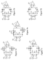
- Resistors 392 and 394 permit easy tuning of the passband central frequency and creation and adjustment of transmission zeros. However, adjusting the resistances does not significantly change the passband bandwidth, which extends essentially from the lower series resonance frequency to the higher parallel resonance frequency of the resonators in the circuit. Narrowing or broadening the passband bandwidth requires adjusting the resonator frequencies. The resonator frequencies may be adjusted by adding additional capacitors and/or inductors in parallel or in series to the resonators. Exemplary circuits including capacitors or inductors to adjust the filter passband are shown in Figures 7a-d .
- Figure 7a shows a circuit in which parallel capacitors 742 and 752 are added to resonators 340 and 350 respectively. Adding a capacitor in parallel increases the total parallel capacitance, and the parallel resonance frequency f p of the resonator 340 and capacitor 742 combination is lowered. Similarly, the parallel resonance frequency f p of the resonator 350 and capacitor 752 combination is lowered. The series resonance frequency f s is unchanged for both resonators. The parallel resonance frequency cannot be less than the series resonance, and the interval between f s and f p is reduced for both resonator-capacitor combinations.
- Figure 7b shows a circuit in which series capacitors 745 and 755 are added to resonators 340 and 350 respectively. Adding a capacitor in series with the resonator increases the series resonance frequency f s of the resonator and capacitor combination. The parallel resonance f p does not change. Again, the interval between the resonances f s and f p is decreased for both resonator-capacitor combinations.
- one capacitor 742 is added in parallel to the first resonator 340 and one capacitor 755 is added in series to the second resonator 350.
- the parallel capacitor 742 moves the parallel resonance frequency of the resonator and capacitor combination 340, 742 downward
- the series capacitor 755 moves the series resonance frequency of the resonator and capacitor combination 350, 755 upward. If the original resonant frequencies of resonator 340 overlap the original resonant frequencies of resonator 350, adding the capacitors 742 and 755 to the circuit can adjust the resonators 340 and 350 so that frequencies f pa and f sb are equal.
- the circuits illustrated in Figures 7a -7c involve only capacitors, and the passband bandwidth is narrowed by adding capacitance.
- inductors may be added in series 744 and 754 to resonators 340 and 350 respectively.
- the series inductor 744 in Figure 7d introduces a second series resonance above the resonances of resonator 340.
- the first series resonance of the whole circuit is less than the original series resonance of resonator 340.
- the inductor does not change the parallel resonance frequency of resonator 340, and the interval between f sa and f pa is thus extended. This modification may be used to introduce more transmission zeros into the filter stopband.
- Figure 7e Adding a parallel inductance to a resonator as shown in Figure 7e introduces a second parallel resonance between 0 and the first series resonance.
- Figure 7e adds inductors 746 and 748 in parallel to both resonators 340 and 350 in the circuit. This modification may be used to introduce other transmission zeros in the filter stopband.
- the series resonance of the combination is unchanged, since it is defined by the resonator 340.
- the effect of a parallel inductor 746 near the original resonance frequencies of the resonator 340 is effectively equivalent to decreasing the capacitance of the resonator.
- the basic parallel resonance frequency of the combination is increased, and the interval between f s and f p is extended.
- a significant broadening of the passband bandwidth can be achieved by using more than one resonator in each arm of the filter circuit.
- Diagrams of circuits incorporating this modification are shown in Figures 8a-8c .
- Additional resonators can be connected in series or in parallel with a resonator of the original circuit of Figure 3a .
- the MBVD equivalent circuit of either connection is a fifth order LC circuit (neglecting loss resistances), exhibiting two series and two parallel resonances.
- the parallel resonances of the combination are the same as the initial parallel resonances, while the series resonances are changed.
- Parallel connection of the resonators in contrast, preserves the initial series resonances but changes the parallel resonances.
- Figures 8a-8c illustrate additional embodiments of the filter circuit that include additional resonators in series or in parallel.
- two resonators are connected in series, 842 and 340, between the positive output port 335 of input amplifier 330 and the positive input port 372 of the output amplifier 370.
- two resonators are connected in parallel, 844 and 340, between the positive output port 335 of input amplifier 330 and the positive input port 372 of the output amplifier 370.
- the two circuits are equivalent, and the choice of implementation may be made on other factors than filter behavior, such as ease of tuning based on the specific design constraints of the implementation.
- Resonator 842 is connected in series with resonator 340 between the positive output port 335 of input amplifier 330 and the positive input port 372 of output amplifier 370.
- Resonator 852 is connected in series with resonator 350 between the negative output port 336 of input amplifier 330 and the positive input port 372 of output amplifier 370.
- the location of the resonance frequencies of the resonators and of their combinations in each part of the circuit follows the basic rule for lattice circuits: the signs of the imaginary parts of the impedances in each section must be different within the passband. This condition requires some matching between the resonance frequencies of the impedances, which can be accomplished by adding capacitors or inductors in series or in parallel to the resonators as discussed earlier. Thus, every resonator in 8a-8c may be accompanied by tuning capacitors or inductors as discussed earlier with regard to Figures 6a-6e .
- variable resistors 392 and 394 can also be used when the circuit contains additional resonators, because the effect of the resistors is independent of the number of resonators in each part of the circuit.
- the use of more than one resonator in each part of the circuit increases the degree of the filter transfer function. The effect is a steeper slope in the transition bands between passband and stopband of the frequency response (more rapid roll-off).
- output amplifier 370 In some applications, particularly when the signals through the filter are expected to be of relatively high power, use of output amplifier 370 could present difficulties. Since output amplifier 370 is a linear circuit element, its power efficiency is limited. For a higher power signal, such as in the last stages of a radio transmitter, the power efficiency is a major consideration in the design of the circuit. In general, however, FBAR filters are preferable for transmitters, since they can transmit relatively large power.
- output amplifier 370 may be replaced by a transformer 970 with transformer ratio 1: N , where N > 1.
- the value of parameter N depends on the load impedance 380 and on the values of the resistors 392 and 394 ( R ).
- the effect of the load resistance 380 can be minimized by a proper choice of the ratio N. If N is chosen so that the input impedance of the transformer together with the load 380 is small enough, the circuit of Figure 9 works similarly to the earlier described embodiment utilizing an output amplifier.
- This alternative embodiment can also be combined with any of the circuit modifications described previously and illustrated in Figures 7 and 8 .
- Transformers are not easily implemented in integrated circuits. However, in some cases, for example when the filter is the last stage of a transmitter, the transformer 970 may be connected externally between the transmitter output and the antenna.
- the filter circuit described herein offers several significant advantages over the conventional FBAR lattice filter.
- the circuit requires half the number of resonators of an equivalent conventional lattice filter.
- the circuit avoids the use of identical resonator pairs required in lattice filters. Tuning of the resonance frequencies of the resonators by using extra capacitors or inductors can be done separately and independently for each resonator in the circuit. In contrast, the tuning of resonance frequencies of identical resonators in the lattice filters must be matched.
- the amplifiers at the input and output of the filter circuit permit a variable gain in the filter passband. The amplifiers separate input and output impedances, allowing operation of the circuit with differing source and load resistances.
- Tuning the passband central frequency of the filter circuit can be accomplished by using two variable resistances in parallel to the output of the first amplifier. These resistances can be connected in parallel to the amplifier output between each output port and the ground; or in series to the amplifier output between each output port and the next resonator terminal.
- the circuit uses the input amplifier output resistances themselves and varies them by changing the quiescent point of the output stage of the first amplifier. Tuning the frequency with variable resistances allows a tuning range similar to that of using variable capacitors connected in series or in parallel to the resonators. Using this tuning method requires less chip area for resistors than would be necessary for inductors and capacitors. In fact, use of the output resistances of the input amplifier can eliminate the need for resistors in the filter circuit.
- Creating transmission zeros and tuning their location in the transfer characteristic of the filter according to the principles of the present invention can be accomplished by adjusting the difference between the resistances of each output port of the input amplifier. Creating and adjusting the location of transmission zeros by this method relaxes the stringent requirements on the values of the resonator equivalent circuit when transmission zeros with prescribed locations are a requirement of the application. Thus, deviations of the elements of the circuit from specified operating parameters can easily be compensated for. Adjusting resistances of the output ports of the input amplifier to introduce transmission zeros does not preclude use of other methods.
- transmission zeros can be introduced and their positions can be roughly defined by specification of the resonator characteristics, by adding extra capacitors or inductors in parallel or in series to the resonators, or by a combination of these methods. Varying the output resistances of the input amplifier can then be used to fine tune the positions of the zeros and the passband boundaries.
- the filter circuit can be modified by adding capacitors or inductors in parallel or in series to one or to both resonators to allow control of the filter passband bandwidth.
- the filter circuit can also be modified by connecting more than one resonator in one or both arms of the circuit to extend the passband bandwidth and increase the slope in the transition bands between the passband and the stopband.
- the resonators may be further combined with capacitors or inductors for more accurate adjustments of their resonance frequencies. Tuning the central passband frequency and creating transmission zeros can also be performed on the modified basic circuit.
- connection of multiple stages of the filter circuit in cascade is also possible, when a steeper transition between passband and stopband is required than could be achieved by a single filter stage. Such a connection does not preclude or substitute for the use of more than one resonator in both arms of the filter circuit. Connecting more stages in cascade would preserve or shrink the pass-band (depending on the design parameters) and would increase roll-off in the stopband.
Landscapes
- Physics & Mathematics (AREA)
- Acoustics & Sound (AREA)
- Networks Using Active Elements (AREA)
- Piezo-Electric Or Mechanical Vibrators, Or Delay Or Filter Circuits (AREA)
Claims (17)
- Filterschaltkreis, der folgendes umfasst:einen Verstärker (330) mit einem positiven Ausgangsanschluss (335) und einem negativen Ausgangsanschluss (336), wobei der genannte Verstärker ein Eingangssignal an einem Eingangsanschluss empfängt und ein differentielles Ausgangssignal an dem genannten positiven Ausgangsanschluss und an dem genannten negativen Ausgangsanschluss erzeugt, wobei der genannte Verstärker einen regelbaren Ausgangswiderstand aufweist;einen ersten Resonator (340) mit ersten und zweiten Anschlüssen, wobei der genannte erste Anschluss mit dem genannten positiven Ausgangsanschluss des genannten Verstärkers verbunden ist, wobei der genannte erste Resonator eine serielle und eine parallele Resonanzfrequenz aufweist;einen zweiten Resonator (350) mit ersten und zweiten Anschlüssen, wobei der genannte erste Anschluss mit dem genannten negativen Ausgangsanschluss des genannten Verstärkers verbunden ist, wobei der genannte erste Resonator eine serielle und eine parallele Resonanzfrequenz aufweist, so dass die serielle Resonanzfrequenz eines des genannten ersten oder des genannten zweiten Resonators im Wesentlichen der parallelen Resonanzfrequenz des anderen Resonators des genannten ersten und zweiten Resonators entspricht;wobei die zweiten Anschlüsse der genannten ersten und zweiten Resonatoren an einem Verbindungsanschluss (360) elektrisch gekoppelt sind, um die dort hindurch verlaufenden Signale zu summieren; und mit einer Puffervorrichtung (370) für den Empfang der durch die ersten und zweiten Resonatoren verlaufenden elektrisch gekoppelten Signale sowie zur Ausgabe eines gefilterten Signals;dadurch gekennzeichnet, dass:der Ausgangswiderstand des genannten Verstärkers regelbar ist, und dass die genannte Puffervorrichtung eine Eingangsimpedanz von im Wesentlichen Null aufweist.
- Filterschaltkreis nach Anspruch 1, wobei die genannte Puffervorrichtung ein Verstärker mit einer Eingangsimpedanz von im Wesentlichen Null ist.
- Filterschaltkreis nach Anspruch 1, wobei die genannte Puffervorrichtung ein Transformator mit einem Transformatorverhältnis von 1:N ist, wobei N > 1 eine Impedanz an dessen Eingang von im Wesentlichen Null sicherstellt.
- Filterschaltkreis nach Anspruch 1, wobei der genannte erste Resonator und der genannte zweite Resonator Film Bulk Acoustic-Resonatoren (FBAR) sind.
- Filterschaltkreis nach Anspruch 1, wobei der genannte Verstärker ein Transkonduktanzverstärker (Operational-Transconductance-Amplifier, OTA) ist.
- Filterschaltkreis nach Anspruch 1, wobei die genannte Puffervorrichtung ein Transresistance-Verstärker oder ein Stromverstärker ist.
- Filterschaltkreis nach Anspruch 1, wobei der genannte Verstärker eine regelbare Verstärkung aufweist.
- Filterschaltkreis nach Anspruch 1, wobei dieser ferner wenigstens einen Widerstand umfasst, der zwischen den genannten positiven Ausgangsanschluss des genannten Verstärkers und den genannten ersten Anschluss des genannten ersten Resonators in Reihe geschaltet ist, und wenigstens einen Widerstand, der zwischen den genannten negativen Ausgangsanschluss des genannten Verstärkers und den ersten Anschluss des genannten zweiten Resonators in Reihe geschaltet ist, wobei die genannten Resonatoren das Frequenzverhalten des Filterschaltkreises regeln.
- Filterschaltkreis nach Anspruch 1, wobei dieser ferner wenigstens einen Widerstand umfasst, der parallel mit dem genannten positiven Ausgangsanschluss des genannten Verstärkers verbunden ist, und wenigstens einen Widerstand, der parallel mit dem genannten negativen Ausgangsanschluss des genannten Verstärkers verbunden ist, wobei die genannten Widerstände das Frequenzverhalten des Filterschaltkreises regeln.
- Filterschaltkreis nach Anspruch 8 oder 9, wobei die genannten Widerstände Regelwiderstände sind.
- Verfahren zum Filtern von Signalen, wobei das Verfahren die folgenden Schritte umfasst:Empfangen eines Signals von einer Signalquelle (310);Erzeugen eines differentiellen Ausgangssignals aus dem empfangenen Signal an einem positiven Ausgangsanschluss (335) und einem negativen Ausgangsanschluss (336) eines Verstärkers (330);Leiten des differentiellen Ausgangssignals durch den positiven Ausgangsanschluss des Verstärkers und einen ersten Resonator (340);Leiten des differentiellen Ausgangssignals durch den negativen Ausgangsanschluss des Verstärkers und einen zweiten Resonator (350);Kombinieren der durch den ersten Resonator und den zweiten Resonator geleiteten Signale, um die dort hindurch verlaufenden Signale zu Summieren; undLeiten des kombinierten Signals durch eine Puffervorrichtung (370), um ein gefiltertes Ausgangssignal zu erzeugen;dadurch gekennzeichnet, dass:das durch den positiven Ausgangsanschluss des Verstärkers verlaufende genannte differentielle Ausgangssignal durch einen ersten Widerstand geleitet wird;das durch den negativen Ausgangsanschluss des Verstärkers verlaufende genannte differentielle Ausgangssignal durch einen zweiten Widerstand geleitet wird;die Puffervorrichtung eine Eingangsimpedanz von im Wesentlichen Null aufweist.
- Verfahren nach Anspruch 11, wobei der Schritt des Regelns der genannten ersten und zweiten Widerstände, um ein gewünschtes Frequenzverhalten zu erreichen, RaRb = ZaZb erfüllt, wobei Ra und Rb die äquivalenten internen Widerstände sind, die entsprechend an den positiven und negativen Ausgangsanschlüssen des Verstärkers vorliegen, wobei Za der komplexe Widerstand des ersten Resonators ist, und wobei Zb der komplexe Widerstand des zweiten Resonators.
- Verfahren nach Anspruch 11, wobei der Schritt des Regelns der genannten ersten und zweiten Widerstände das Anlegen einer Vorspannung an den Verstärker aufweist.
- Verfahren nach Anspruch 11, wobei der Schritt des Regelns der internen Widerstände zum Erreichen eines gewünschten Filterfrequenzverhaltens das Leiten des differentiellen Ausgangssignals durch wenigstens einen Widerstand aufweist, wobei der genannte Widerstand entweder 1) in Reihe verbunden ist zwischen dem genannten positiven Ausgangsanschluss des genannten Verstärkers und des ersten Resonators, und wobei wenigstens ein Widerstand in Reihe verbunden ist zwischen den genannten negativen Ausgangsanschluss des Verstärkers und den zweiten Resonator; oder 2) parallel mit dem genannten positiven Ausgangsanschluss des genannten Verstärkers verbunden ist, und wobei wenigstens ein Widerstand parallel mit dem genannten negativen Ausgangsanschluss des genannten Verstärkers verbunden ist.
- Verfahren nach Anspruch 11, wobei dieses ferner den Schritt des Leitens des differentiellen Ausgangssignals durch einen ersten Widerstand an dem positiven Ausgangsanschluss des Verstärkers umfasst und des Leitens des differentiellen Ausgangssignals durch einen zweiten Widerstand an dem negativen Ausgangsanschluss des Verstärkers, wobei der Widerstand des zweiten Widerstands sich von dem Widerstand des genannten ersten Widerstands unterscheidet, um in einer Filterübertragungsfunktion Übertragungsnullstellen zu erzeugen.
- Verfahren nach Anspruch 11, wobei dieses ferner den Schritt des Leitens des differentiellen Ausgangssignals von einem positiven Ausgangsanschluss mit einem ersten Widerstand sowie des Erzeugens des differentiellen Ausgangssignals von einem negativen Ausgangsanschluss mit einem zweiten Widerstand umfasst, der sich von dem ersten Widerstand unterscheidet, um in einer Filterübertragungsfunktion Übertragungsnullstellen zu erzeugen.
- Verfahren nach Anspruch 1 oder 16, wobei dieses ferner das Regeln der Widerstandswerte der zwei sich unterscheidenden Widerstände umfasst, um die Werte der Übertragungsnullstellen in der Filterübertragungsfunktion zu regeln.
Applications Claiming Priority (1)
| Application Number | Priority Date | Filing Date | Title |
|---|---|---|---|
| PCT/IB2009/006083 WO2010150037A1 (en) | 2009-06-26 | 2009-06-26 | Filter circuit |
Publications (2)
| Publication Number | Publication Date |
|---|---|
| EP2446532A1 EP2446532A1 (de) | 2012-05-02 |
| EP2446532B1 true EP2446532B1 (de) | 2016-08-10 |
Family
ID=41682243
Family Applications (1)
| Application Number | Title | Priority Date | Filing Date |
|---|---|---|---|
| EP09785970.6A Not-in-force EP2446532B1 (de) | 2009-06-26 | 2009-06-26 | Filterkreis |
Country Status (4)
| Country | Link |
|---|---|
| US (1) | US8686788B2 (de) |
| EP (1) | EP2446532B1 (de) |
| KR (1) | KR101366065B1 (de) |
| WO (1) | WO2010150037A1 (de) |
Families Citing this family (3)
| Publication number | Priority date | Publication date | Assignee | Title |
|---|---|---|---|---|
| EP3346606B1 (de) | 2009-10-23 | 2019-12-04 | Telefonaktiebolaget LM Ericsson (publ) | Passiver mischer mit reduzierter intermodulation zweiter ordnung |
| US9979377B1 (en) * | 2013-05-28 | 2018-05-22 | Qorvo Us, Inc. | Frequency filter |
| GB2598594A (en) | 2020-09-03 | 2022-03-09 | Novelda As | Filter |
Family Cites Families (7)
| Publication number | Priority date | Publication date | Assignee | Title |
|---|---|---|---|---|
| GB802006A (en) * | 1955-07-18 | 1958-09-24 | Marconi Wireless Telegraph Co | Improvements in or relating to crystal filters |
| US3566314A (en) | 1968-02-27 | 1971-02-23 | Bell Telephone Labor Inc | Crystal band-pass filter with controlled attenuation between passbands |
| JPS55128913A (en) * | 1979-03-28 | 1980-10-06 | Nippon Dempa Kogyo Co Ltd | Piezoelectric band pass filter |
| US5777527A (en) | 1996-10-31 | 1998-07-07 | Motorola, Inc. | Method and apparatus for coupling a differential signal to an unbalanced port |
| US6844792B1 (en) | 2002-05-15 | 2005-01-18 | Zeevo | Single ended tuning of a differential power amplifier output |
| JP2007036856A (ja) * | 2005-07-28 | 2007-02-08 | Fujitsu Media Device Kk | 共振器、フィルタおよびアンテナ分波器 |
| US7808310B2 (en) | 2007-11-28 | 2010-10-05 | Infineon Technologies, Ag | Differential band-pass filter having symmetrically interwoven inductors |
-
2009
- 2009-06-26 EP EP09785970.6A patent/EP2446532B1/de not_active Not-in-force
- 2009-06-26 US US13/387,117 patent/US8686788B2/en not_active Expired - Fee Related
- 2009-06-26 KR KR1020127002181A patent/KR101366065B1/ko not_active Expired - Fee Related
- 2009-06-26 WO PCT/IB2009/006083 patent/WO2010150037A1/en not_active Ceased
Also Published As
| Publication number | Publication date |
|---|---|
| WO2010150037A1 (en) | 2010-12-29 |
| US8686788B2 (en) | 2014-04-01 |
| KR101366065B1 (ko) | 2014-02-25 |
| EP2446532A1 (de) | 2012-05-02 |
| US20120161862A1 (en) | 2012-06-28 |
| KR20120054588A (ko) | 2012-05-30 |
Similar Documents
| Publication | Publication Date | Title |
|---|---|---|
| US10931262B2 (en) | Tunable resonator element, filter circuit and method | |
| US6670866B2 (en) | Bulk acoustic wave resonator with two piezoelectric layers as balun in filters and duplexers | |
| KR102025982B1 (ko) | 튜닝 가능 공진기 소자, 필터 회로 및 방법 | |
| JP4523637B2 (ja) | 結合baw共振器をベースとする送受切換器 | |
| US9325294B2 (en) | Microwave acoustic wave filters | |
| WO2019065274A1 (ja) | フィルタ装置、マルチプレクサ、高周波フロントエンド回路および通信装置 | |
| US10727810B2 (en) | Radio-frequency filter, multiplexer, radio-frequency front-end circuit, and communication device | |
| WO2018097203A1 (ja) | 弾性波フィルタ装置、マルチプレクサ、高周波フロントエンド回路および通信装置 | |
| US8686788B2 (en) | Filter circuit | |
| Akgul et al. | A passband-corrected high rejection channel-select micromechanical disk filter | |
| US20050093652A1 (en) | Size scaling of film bulk acoustic resonator (FBAR) filters using impedance transformer (IT) or balun | |
| CN103262411B (zh) | 滤波器件 | |
| WO2004066494A1 (en) | Resonator filter structure with improved balance | |
| TW202213941A (zh) | 濾波器 |
Legal Events
| Date | Code | Title | Description |
|---|---|---|---|
| PUAI | Public reference made under article 153(3) epc to a published international application that has entered the european phase |
Free format text: ORIGINAL CODE: 0009012 |
|
| 17P | Request for examination filed |
Effective date: 20120125 |
|
| AK | Designated contracting states |
Kind code of ref document: A1 Designated state(s): AT BE BG CH CY CZ DE DK EE ES FI FR GB GR HR HU IE IS IT LI LT LU LV MC MK MT NL NO PL PT RO SE SI SK TR |
|
| DAX | Request for extension of the european patent (deleted) | ||
| 17Q | First examination report despatched |
Effective date: 20140716 |
|
| GRAP | Despatch of communication of intention to grant a patent |
Free format text: ORIGINAL CODE: EPIDOSNIGR1 |
|
| INTG | Intention to grant announced |
Effective date: 20160209 |
|
| GRAS | Grant fee paid |
Free format text: ORIGINAL CODE: EPIDOSNIGR3 |
|
| GRAA | (expected) grant |
Free format text: ORIGINAL CODE: 0009210 |
|
| AK | Designated contracting states |
Kind code of ref document: B1 Designated state(s): AT BE BG CH CY CZ DE DK EE ES FI FR GB GR HR HU IE IS IT LI LT LU LV MC MK MT NL NO PL PT RO SE SI SK TR |
|
| REG | Reference to a national code |
Ref country code: GB Ref legal event code: FG4D |
|
| REG | Reference to a national code |
Ref country code: CH Ref legal event code: EP Ref country code: AT Ref legal event code: REF Ref document number: 819851 Country of ref document: AT Kind code of ref document: T Effective date: 20160815 |
|
| REG | Reference to a national code |
Ref country code: IE Ref legal event code: FG4D |
|
| REG | Reference to a national code |
Ref country code: DE Ref legal event code: R096 Ref document number: 602009040303 Country of ref document: DE |
|
| REG | Reference to a national code |
Ref country code: LT Ref legal event code: MG4D |
|
| REG | Reference to a national code |
Ref country code: NL Ref legal event code: MP Effective date: 20160810 |
|
| REG | Reference to a national code |
Ref country code: AT Ref legal event code: MK05 Ref document number: 819851 Country of ref document: AT Kind code of ref document: T Effective date: 20160810 |
|
| PG25 | Lapsed in a contracting state [announced via postgrant information from national office to epo] |
Ref country code: NL Free format text: LAPSE BECAUSE OF FAILURE TO SUBMIT A TRANSLATION OF THE DESCRIPTION OR TO PAY THE FEE WITHIN THE PRESCRIBED TIME-LIMIT Effective date: 20160810 Ref country code: IT Free format text: LAPSE BECAUSE OF FAILURE TO SUBMIT A TRANSLATION OF THE DESCRIPTION OR TO PAY THE FEE WITHIN THE PRESCRIBED TIME-LIMIT Effective date: 20160810 Ref country code: FI Free format text: LAPSE BECAUSE OF FAILURE TO SUBMIT A TRANSLATION OF THE DESCRIPTION OR TO PAY THE FEE WITHIN THE PRESCRIBED TIME-LIMIT Effective date: 20160810 Ref country code: NO Free format text: LAPSE BECAUSE OF FAILURE TO SUBMIT A TRANSLATION OF THE DESCRIPTION OR TO PAY THE FEE WITHIN THE PRESCRIBED TIME-LIMIT Effective date: 20161110 Ref country code: IS Free format text: LAPSE BECAUSE OF FAILURE TO SUBMIT A TRANSLATION OF THE DESCRIPTION OR TO PAY THE FEE WITHIN THE PRESCRIBED TIME-LIMIT Effective date: 20161210 Ref country code: HR Free format text: LAPSE BECAUSE OF FAILURE TO SUBMIT A TRANSLATION OF THE DESCRIPTION OR TO PAY THE FEE WITHIN THE PRESCRIBED TIME-LIMIT Effective date: 20160810 Ref country code: LT Free format text: LAPSE BECAUSE OF FAILURE TO SUBMIT A TRANSLATION OF THE DESCRIPTION OR TO PAY THE FEE WITHIN THE PRESCRIBED TIME-LIMIT Effective date: 20160810 |
|
| PG25 | Lapsed in a contracting state [announced via postgrant information from national office to epo] |
Ref country code: PT Free format text: LAPSE BECAUSE OF FAILURE TO SUBMIT A TRANSLATION OF THE DESCRIPTION OR TO PAY THE FEE WITHIN THE PRESCRIBED TIME-LIMIT Effective date: 20161212 Ref country code: ES Free format text: LAPSE BECAUSE OF FAILURE TO SUBMIT A TRANSLATION OF THE DESCRIPTION OR TO PAY THE FEE WITHIN THE PRESCRIBED TIME-LIMIT Effective date: 20160810 Ref country code: GR Free format text: LAPSE BECAUSE OF FAILURE TO SUBMIT A TRANSLATION OF THE DESCRIPTION OR TO PAY THE FEE WITHIN THE PRESCRIBED TIME-LIMIT Effective date: 20161111 Ref country code: LV Free format text: LAPSE BECAUSE OF FAILURE TO SUBMIT A TRANSLATION OF THE DESCRIPTION OR TO PAY THE FEE WITHIN THE PRESCRIBED TIME-LIMIT Effective date: 20160810 Ref country code: AT Free format text: LAPSE BECAUSE OF FAILURE TO SUBMIT A TRANSLATION OF THE DESCRIPTION OR TO PAY THE FEE WITHIN THE PRESCRIBED TIME-LIMIT Effective date: 20160810 Ref country code: PL Free format text: LAPSE BECAUSE OF FAILURE TO SUBMIT A TRANSLATION OF THE DESCRIPTION OR TO PAY THE FEE WITHIN THE PRESCRIBED TIME-LIMIT Effective date: 20160810 Ref country code: SE Free format text: LAPSE BECAUSE OF FAILURE TO SUBMIT A TRANSLATION OF THE DESCRIPTION OR TO PAY THE FEE WITHIN THE PRESCRIBED TIME-LIMIT Effective date: 20160810 |
|
| PG25 | Lapsed in a contracting state [announced via postgrant information from national office to epo] |
Ref country code: RO Free format text: LAPSE BECAUSE OF FAILURE TO SUBMIT A TRANSLATION OF THE DESCRIPTION OR TO PAY THE FEE WITHIN THE PRESCRIBED TIME-LIMIT Effective date: 20160810 Ref country code: EE Free format text: LAPSE BECAUSE OF FAILURE TO SUBMIT A TRANSLATION OF THE DESCRIPTION OR TO PAY THE FEE WITHIN THE PRESCRIBED TIME-LIMIT Effective date: 20160810 |
|
| REG | Reference to a national code |
Ref country code: DE Ref legal event code: R097 Ref document number: 602009040303 Country of ref document: DE |
|
| PG25 | Lapsed in a contracting state [announced via postgrant information from national office to epo] |
Ref country code: CZ Free format text: LAPSE BECAUSE OF FAILURE TO SUBMIT A TRANSLATION OF THE DESCRIPTION OR TO PAY THE FEE WITHIN THE PRESCRIBED TIME-LIMIT Effective date: 20160810 Ref country code: DK Free format text: LAPSE BECAUSE OF FAILURE TO SUBMIT A TRANSLATION OF THE DESCRIPTION OR TO PAY THE FEE WITHIN THE PRESCRIBED TIME-LIMIT Effective date: 20160810 Ref country code: BE Free format text: LAPSE BECAUSE OF FAILURE TO SUBMIT A TRANSLATION OF THE DESCRIPTION OR TO PAY THE FEE WITHIN THE PRESCRIBED TIME-LIMIT Effective date: 20160810 Ref country code: BG Free format text: LAPSE BECAUSE OF FAILURE TO SUBMIT A TRANSLATION OF THE DESCRIPTION OR TO PAY THE FEE WITHIN THE PRESCRIBED TIME-LIMIT Effective date: 20161110 Ref country code: SK Free format text: LAPSE BECAUSE OF FAILURE TO SUBMIT A TRANSLATION OF THE DESCRIPTION OR TO PAY THE FEE WITHIN THE PRESCRIBED TIME-LIMIT Effective date: 20160810 |
|
| PLBE | No opposition filed within time limit |
Free format text: ORIGINAL CODE: 0009261 |
|
| STAA | Information on the status of an ep patent application or granted ep patent |
Free format text: STATUS: NO OPPOSITION FILED WITHIN TIME LIMIT |
|
| 26N | No opposition filed |
Effective date: 20170511 |
|
| PG25 | Lapsed in a contracting state [announced via postgrant information from national office to epo] |
Ref country code: SI Free format text: LAPSE BECAUSE OF FAILURE TO SUBMIT A TRANSLATION OF THE DESCRIPTION OR TO PAY THE FEE WITHIN THE PRESCRIBED TIME-LIMIT Effective date: 20160810 |
|
| REG | Reference to a national code |
Ref country code: FR Ref legal event code: PLFP Year of fee payment: 9 |
|
| PG25 | Lapsed in a contracting state [announced via postgrant information from national office to epo] |
Ref country code: MC Free format text: LAPSE BECAUSE OF FAILURE TO SUBMIT A TRANSLATION OF THE DESCRIPTION OR TO PAY THE FEE WITHIN THE PRESCRIBED TIME-LIMIT Effective date: 20160810 |
|
| REG | Reference to a national code |
Ref country code: CH Ref legal event code: PL |
|
| PG25 | Lapsed in a contracting state [announced via postgrant information from national office to epo] |
Ref country code: LU Free format text: LAPSE BECAUSE OF NON-PAYMENT OF DUE FEES Effective date: 20170626 Ref country code: LI Free format text: LAPSE BECAUSE OF NON-PAYMENT OF DUE FEES Effective date: 20170630 Ref country code: CH Free format text: LAPSE BECAUSE OF NON-PAYMENT OF DUE FEES Effective date: 20170630 |
|
| REG | Reference to a national code |
Ref country code: FR Ref legal event code: PLFP Year of fee payment: 10 |
|
| PG25 | Lapsed in a contracting state [announced via postgrant information from national office to epo] |
Ref country code: MT Free format text: LAPSE BECAUSE OF NON-PAYMENT OF DUE FEES Effective date: 20170626 |
|
| PG25 | Lapsed in a contracting state [announced via postgrant information from national office to epo] |
Ref country code: HU Free format text: LAPSE BECAUSE OF FAILURE TO SUBMIT A TRANSLATION OF THE DESCRIPTION OR TO PAY THE FEE WITHIN THE PRESCRIBED TIME-LIMIT; INVALID AB INITIO Effective date: 20090626 |
|
| PGFP | Annual fee paid to national office [announced via postgrant information from national office to epo] |
Ref country code: IE Payment date: 20190610 Year of fee payment: 11 Ref country code: DE Payment date: 20190612 Year of fee payment: 11 |
|
| PGFP | Annual fee paid to national office [announced via postgrant information from national office to epo] |
Ref country code: FR Payment date: 20190604 Year of fee payment: 11 |
|
| PG25 | Lapsed in a contracting state [announced via postgrant information from national office to epo] |
Ref country code: CY Free format text: LAPSE BECAUSE OF NON-PAYMENT OF DUE FEES Effective date: 20160810 |
|
| PGFP | Annual fee paid to national office [announced via postgrant information from national office to epo] |
Ref country code: GB Payment date: 20190626 Year of fee payment: 11 |
|
| PG25 | Lapsed in a contracting state [announced via postgrant information from national office to epo] |
Ref country code: MK Free format text: LAPSE BECAUSE OF FAILURE TO SUBMIT A TRANSLATION OF THE DESCRIPTION OR TO PAY THE FEE WITHIN THE PRESCRIBED TIME-LIMIT Effective date: 20160810 |
|
| PG25 | Lapsed in a contracting state [announced via postgrant information from national office to epo] |
Ref country code: TR Free format text: LAPSE BECAUSE OF FAILURE TO SUBMIT A TRANSLATION OF THE DESCRIPTION OR TO PAY THE FEE WITHIN THE PRESCRIBED TIME-LIMIT Effective date: 20160810 |
|
| REG | Reference to a national code |
Ref country code: DE Ref legal event code: R119 Ref document number: 602009040303 Country of ref document: DE |
|
| GBPC | Gb: european patent ceased through non-payment of renewal fee |
Effective date: 20200626 |
|
| PG25 | Lapsed in a contracting state [announced via postgrant information from national office to epo] |
Ref country code: FR Free format text: LAPSE BECAUSE OF NON-PAYMENT OF DUE FEES Effective date: 20200630 Ref country code: GB Free format text: LAPSE BECAUSE OF NON-PAYMENT OF DUE FEES Effective date: 20200626 Ref country code: IE Free format text: LAPSE BECAUSE OF NON-PAYMENT OF DUE FEES Effective date: 20200626 |
|
| PG25 | Lapsed in a contracting state [announced via postgrant information from national office to epo] |
Ref country code: DE Free format text: LAPSE BECAUSE OF NON-PAYMENT OF DUE FEES Effective date: 20210101 |