EP2447596A2 - Lichtemittierende Vorrichtung und Beleuchtungsvorrichtung - Google Patents
Lichtemittierende Vorrichtung und Beleuchtungsvorrichtung Download PDFInfo
- Publication number
- EP2447596A2 EP2447596A2 EP11186669A EP11186669A EP2447596A2 EP 2447596 A2 EP2447596 A2 EP 2447596A2 EP 11186669 A EP11186669 A EP 11186669A EP 11186669 A EP11186669 A EP 11186669A EP 2447596 A2 EP2447596 A2 EP 2447596A2
- Authority
- EP
- European Patent Office
- Prior art keywords
- light emitting
- mounting pads
- lead pattern
- emitting elements
- substrate
- Prior art date
- Legal status (The legal status is an assumption and is not a legal conclusion. Google has not performed a legal analysis and makes no representation as to the accuracy of the status listed.)
- Withdrawn
Links
Images


Classifications
-
- F—MECHANICAL ENGINEERING; LIGHTING; HEATING; WEAPONS; BLASTING
- F21—LIGHTING
- F21K—NON-ELECTRIC LIGHT SOURCES USING LUMINESCENCE; LIGHT SOURCES USING ELECTROCHEMILUMINESCENCE; LIGHT SOURCES USING CHARGES OF COMBUSTIBLE MATERIAL; LIGHT SOURCES USING SEMICONDUCTOR DEVICES AS LIGHT-GENERATING ELEMENTS; LIGHT SOURCES NOT OTHERWISE PROVIDED FOR
- F21K9/00—Light sources using semiconductor devices as light-generating elements, e.g. using light-emitting diodes [LED] or lasers
-
- H—ELECTRICITY
- H10—SEMICONDUCTOR DEVICES; ELECTRIC SOLID-STATE DEVICES NOT OTHERWISE PROVIDED FOR
- H10H—INORGANIC LIGHT-EMITTING SEMICONDUCTOR DEVICES HAVING POTENTIAL BARRIERS
- H10H20/00—Individual inorganic light-emitting semiconductor devices having potential barriers, e.g. light-emitting diodes [LED]
- H10H20/80—Constructional details
- H10H20/85—Packages
- H10H20/858—Means for heat extraction or cooling
- H10H20/8581—Means for heat extraction or cooling characterised by their material
-
- F—MECHANICAL ENGINEERING; LIGHTING; HEATING; WEAPONS; BLASTING
- F21—LIGHTING
- F21V—FUNCTIONAL FEATURES OR DETAILS OF LIGHTING DEVICES OR SYSTEMS THEREOF; STRUCTURAL COMBINATIONS OF LIGHTING DEVICES WITH OTHER ARTICLES, NOT OTHERWISE PROVIDED FOR
- F21V29/00—Protecting lighting devices from thermal damage; Cooling or heating arrangements specially adapted for lighting devices or systems
- F21V29/50—Cooling arrangements
- F21V29/502—Cooling arrangements characterised by the adaptation for cooling of specific components
- F21V29/505—Cooling arrangements characterised by the adaptation for cooling of specific components of reflectors
-
- H—ELECTRICITY
- H05—ELECTRIC TECHNIQUES NOT OTHERWISE PROVIDED FOR
- H05K—PRINTED CIRCUITS; CASINGS OR CONSTRUCTIONAL DETAILS OF ELECTRIC APPARATUS; MANUFACTURE OF ASSEMBLAGES OF ELECTRICAL COMPONENTS
- H05K1/00—Printed circuits
- H05K1/02—Details
- H05K1/0201—Thermal arrangements, e.g. for cooling, heating or preventing overheating
- H05K1/0203—Cooling of mounted components
- H05K1/0209—External configuration of printed circuit board adapted for heat dissipation, e.g. lay-out of conductors, coatings
-
- H—ELECTRICITY
- H10—SEMICONDUCTOR DEVICES; ELECTRIC SOLID-STATE DEVICES NOT OTHERWISE PROVIDED FOR
- H10H—INORGANIC LIGHT-EMITTING SEMICONDUCTOR DEVICES HAVING POTENTIAL BARRIERS
- H10H20/00—Individual inorganic light-emitting semiconductor devices having potential barriers, e.g. light-emitting diodes [LED]
- H10H20/80—Constructional details
- H10H20/85—Packages
- H10H20/8506—Containers
-
- F—MECHANICAL ENGINEERING; LIGHTING; HEATING; WEAPONS; BLASTING
- F21—LIGHTING
- F21Y—INDEXING SCHEME ASSOCIATED WITH SUBCLASSES F21K, F21L, F21S and F21V, RELATING TO THE FORM OR THE KIND OF THE LIGHT SOURCES OR OF THE COLOUR OF THE LIGHT EMITTED
- F21Y2103/00—Elongate light sources, e.g. fluorescent tubes
- F21Y2103/10—Elongate light sources, e.g. fluorescent tubes comprising a linear array of point-like light-generating elements
-
- F—MECHANICAL ENGINEERING; LIGHTING; HEATING; WEAPONS; BLASTING
- F21—LIGHTING
- F21Y—INDEXING SCHEME ASSOCIATED WITH SUBCLASSES F21K, F21L, F21S and F21V, RELATING TO THE FORM OR THE KIND OF THE LIGHT SOURCES OR OF THE COLOUR OF THE LIGHT EMITTED
- F21Y2105/00—Planar light sources
- F21Y2105/10—Planar light sources comprising a two-dimensional [2D] array of point-like light-generating elements
-
- F—MECHANICAL ENGINEERING; LIGHTING; HEATING; WEAPONS; BLASTING
- F21—LIGHTING
- F21Y—INDEXING SCHEME ASSOCIATED WITH SUBCLASSES F21K, F21L, F21S and F21V, RELATING TO THE FORM OR THE KIND OF THE LIGHT SOURCES OR OF THE COLOUR OF THE LIGHT EMITTED
- F21Y2115/00—Light-generating elements of semiconductor light sources
- F21Y2115/10—Light-emitting diodes [LED]
-
- H—ELECTRICITY
- H05—ELECTRIC TECHNIQUES NOT OTHERWISE PROVIDED FOR
- H05K—PRINTED CIRCUITS; CASINGS OR CONSTRUCTIONAL DETAILS OF ELECTRIC APPARATUS; MANUFACTURE OF ASSEMBLAGES OF ELECTRICAL COMPONENTS
- H05K1/00—Printed circuits
- H05K1/02—Details
- H05K1/11—Printed elements for providing electric connections to or between printed circuits
- H05K1/111—Pads for surface mounting, e.g. lay-out
- H05K1/112—Pads for surface mounting, e.g. lay-out directly combined with via connections
- H05K1/113—Via provided in pad; Pad over filled via
-
- H—ELECTRICITY
- H05—ELECTRIC TECHNIQUES NOT OTHERWISE PROVIDED FOR
- H05K—PRINTED CIRCUITS; CASINGS OR CONSTRUCTIONAL DETAILS OF ELECTRIC APPARATUS; MANUFACTURE OF ASSEMBLAGES OF ELECTRICAL COMPONENTS
- H05K2201/00—Indexing scheme relating to printed circuits covered by H05K1/00
- H05K2201/10—Details of components or other objects attached to or integrated in a printed circuit board
- H05K2201/10007—Types of components
- H05K2201/10106—Light emitting diode [LED]
-
- H—ELECTRICITY
- H05—ELECTRIC TECHNIQUES NOT OTHERWISE PROVIDED FOR
- H05K—PRINTED CIRCUITS; CASINGS OR CONSTRUCTIONAL DETAILS OF ELECTRIC APPARATUS; MANUFACTURE OF ASSEMBLAGES OF ELECTRICAL COMPONENTS
- H05K2201/00—Indexing scheme relating to printed circuits covered by H05K1/00
- H05K2201/20—Details of printed circuits not provided for in H05K2201/01 - H05K2201/10
- H05K2201/2054—Light-reflecting surface, e.g. conductors, substrates, coatings, dielectrics
-
- H—ELECTRICITY
- H05—ELECTRIC TECHNIQUES NOT OTHERWISE PROVIDED FOR
- H05K—PRINTED CIRCUITS; CASINGS OR CONSTRUCTIONAL DETAILS OF ELECTRIC APPARATUS; MANUFACTURE OF ASSEMBLAGES OF ELECTRICAL COMPONENTS
- H05K3/00—Apparatus or processes for manufacturing printed circuits
- H05K3/22—Secondary treatment of printed circuits
- H05K3/28—Applying non-metallic protective coatings
- H05K3/284—Applying non-metallic protective coatings for encapsulating mounted components
-
- H—ELECTRICITY
- H10—SEMICONDUCTOR DEVICES; ELECTRIC SOLID-STATE DEVICES NOT OTHERWISE PROVIDED FOR
- H10W—GENERIC PACKAGES, INTERCONNECTIONS, CONNECTORS OR OTHER CONSTRUCTIONAL DETAILS OF DEVICES COVERED BY CLASS H10
- H10W72/00—Interconnections or connectors in packages
- H10W72/50—Bond wires
- H10W72/551—Materials of bond wires
- H10W72/552—Materials of bond wires comprising metals or metalloids, e.g. silver
- H10W72/5522—Materials of bond wires comprising metals or metalloids, e.g. silver comprising gold [Au]
-
- H—ELECTRICITY
- H10—SEMICONDUCTOR DEVICES; ELECTRIC SOLID-STATE DEVICES NOT OTHERWISE PROVIDED FOR
- H10W—GENERIC PACKAGES, INTERCONNECTIONS, CONNECTORS OR OTHER CONSTRUCTIONAL DETAILS OF DEVICES COVERED BY CLASS H10
- H10W72/00—Interconnections or connectors in packages
- H10W72/851—Dispositions of multiple connectors or interconnections
- H10W72/874—On different surfaces
- H10W72/884—Die-attach connectors and bond wires
Definitions
- Embodiments described herein relate generally to a light emitting device and an illumination device using a light emitting element such as an LED as a light source.
- LEDs have been used as light sources of illumination devices.
- Such light sources include many bare LED chips disposed on a substrate and mounted to the substrate by electrically connecting the LED chips to a lead pattern by bonding wires. Then, the substrate is multiply included in an LED illumination device by being embedded in a main body made of a metal such as aluminum, etc.
- lighting control of the LED is performed by power being supplied by a lighting device connected to an alternating-current power source.
- the main body made of the metal has a grounding potential by being grounded.
- a light emitting device in general, includes a substrate, a lead pattern and a plurality of mounting pads, and a plurality of light emitting elements.
- the substrate includes an insulating layer.
- the lead pattern and the plurality of mounting pads are formed on a surface of the substrate.
- the lead pattern and the plurality of mounting pads are conductive.
- the plurality of mounting pads are configured not to electrically conduct.
- the lead pattern is configured to electrically conduct.
- the plurality of light emitting elements are mounted on the mounting pads and electrically connected to the lead pattern.
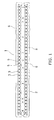
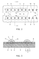
- a light emitting device 1 includes a substrate 2, mounting pads 3 and a lead pattern 4 that are formed on a surface of the substrate 2, multiple light emitting elements 5, and a sealing member 6.
- the substrate 2 is insulative.
- the substrate 2 is an insulating layer made of an insulating material such as a glass epoxy resin, etc., and is formed in a slender rectangular configuration.
- the length dimension is about 250 mm to 300 mm; and the width dimension is about 10 mm to 32 mm. It is favorable for the thickness dimension of the substrate 2 to be not less than 0.5 mm and not more than 1.8 mm; and a thickness dimension of about 1 mm is used in this embodiment.
- the configuration of the substrate 2 is not limited to a rectangular configuration. A square configuration or a circular configuration may be used. A ceramic material or another synthetic resin material may be used as the material of the substrate 2.
- a substrate made of a metal may be used as the substrate 2, where a base plate made of a metal material such as aluminum, etc., that has good thermal conductivity and excellent heat dissipation is provided and an insulating layer is stacked on one surface of the base plate.
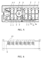
- FIG. 4 and FIG. 5 illustrate the mounting pads 3 and the lead pattern 4 formed on the surface of the substrate 2.
- the mounting pads 3 and the lead pattern 4 are conductive and have a three layer configuration as described below.
- the layer structure of the mounting pads 3 is the same as the layer structure of the lead pattern 4. In other words, layers that are formed from the same material and have the same thicknesses are stacked in the same order.
- the mounting pad 3 is the portion where the light emitting element 5 is mounted; the mounting pad 3 has a substantially circular configuration; and a pair of notches 3a are made in the mounting pad 3 by opposing portions of the circumference (in FIG. 5 , the portion on the upper side and the portion on the lower side) being notched in arc configurations.
- the power supply members 4a extend from the lead pattern 4 and are disposed inside the pair of notches 3a. In other words, the power supply members 4a enter the notches 3a.
- the notch 3a and the power supply member 4a are insulated from each other by being separated by a prescribed distance.
- the mounting pads 3 are multiply formed in a column along the longitudinal direction of the substrate 2. Specifically, there are two columns along the longitudinal direction of the substrate 2; and one column has thirty-five mounting pads 3 disposed at substantially uniform spacing.
- the mounting pad 3 is a nonconducting pad that is conductive but is configured not to electrically conduct and is electrically isolated.
- the surface of the mounting pad 3 functions as a reflective layer and functions as a heat dissipation layer that dissipates heat generated by the light emitting element 5.
- the lead pattern 4 is included in a power supply path, has a pattern of fine leads, and can supply power from a power source side to the light emitting elements 5.
- the power supply members 4a to which the light emitting elements 5 are connected, are provided in the lead pattern 4.
- a pattern of a metal layer, e.g., a copper foil 7, that dissipates the heat of the substrate 2 is formed over the entire surface of each of the regions substantially surrounded by the mounting pads 3 and the lead pattern 4.
- the copper foil 7 is insulated from the mounting pads 3 and the lead pattern 4. Thereby, the thermal uniformity of the entire substrate 2 can be increased and the heat dissipation performance can be improved.
- the mounting pads 3 and the lead pattern 4 have a three layer configuration in which a copper pattern is provided by etching as a first layer A on the surface of the substrate 2.
- Nickel (Ni) is electroplated as a second layer B on the copper pattern layer; and silver (Ag) is electroplated as a third layer C. Therefore, the third layer C, i.e., the surface layer, is a silver (Ag) plating layer.
- the upper surfaces of the mounting pads 3 and the lead pattern 4 have a metallic luster and a high total luminous reflectance of 90%.
- the electroplating it is favorable to form the nickel (Ni) of the second layer B with a film thickness not less than 5 ⁇ m and the silver (Ag) of the third layer C with a film thickness not less than 1 ⁇ m.
- Ni nickel
- Ag silver
- a white resist layer 8 that has a high reflectance is stacked on substantially the entire surface of the surface layer of the substrate 2 except for the regions of the mounting pads 3 used as the mounting regions of the light emitting elements 5, the regions of the power supply members 4a of the lead pattern 4, and the mounting portions of parts.
- the multiple light emitting elements 5 are made of bare LED chips.
- a chip configured to emit blue light, for example, is used as the bare LED chip to emit whitish light from a light emitting unit.
- the bare LED chips are bonded onto the mounting pads 3 using a silicone resin-type insulative bonding agent 9.
- the bare LED chip is, for example, an InGaN-type element formed by stacking a light emitting layer on a transparent sapphire element substrate, where the light emitting layer is formed by sequentially stacking an n-type nitride semiconductor layer, an InGaN light emitting layer, and a p-type nitride semiconductor layer.
- the electrodes for causing a current to flow in the light emitting layer include a positive-side electrode formed of a p-type electrode pad on the p-type nitride semiconductor layer and a negative-side electrode formed of an n-type electrode pad on the n-type nitride semiconductor layer.
- the bonding wires 10 are made of fine gold (Au) wires and are connected via bumps (not illustrated) having a main component of gold (Au) to increase the mounting strength and reduce damage of the bare LED chips.
- the multiple light emitting elements 5 are mounted on the mounting pads 3 in substantially central portions of the substantially circular configurations of the mounting pads 3; and the light emitting elements 5 and the mounting pads 3 are disposed with a one-to-one relationship. Accordingly, two columns of light emitting elements are formed by mounting the light emitting elements 5 on the multiple mounting pads 3 arranged in the longitudinal direction.
- the power supply members 4a it is favorable for the power supply members 4a to be formed with a surface area in a range of 1 to 2 times the surface area of the upper surface of the bare LED chip. In the case of being less than a factor of 1, there is a possibility that discrepancies may occur during the bonding and during use because the reliability of the bonding of the bonding wires 10 is poor. In the case of being greater than a factor of 2, the surface area of not only the power supply members 4a but also the lead pattern 4 increases as an entirety; and there is a tendency for erroneous lighting of the light emitting elements 5 to occur easily as described below.
- the dimensions of the upper surface of the bare LED chip are 0.5 mm by 0.3 mm; the surface area of the upper surface of the bare LED chip is 0.15 mm 2 ; and the surface area of the power supply member 4a is 0.25 mm 2 .
- the light emitting elements 5 thus disposed are connected from a positive-side power source through the lead pattern 4, through one of the power supply members 4a, and through the bonding wire 10 to the positive-side electrode of the light emitting element 5 and from the negative-side electrode of the light emitting element 5 through the bonding wire 10 to one other of the power supply members 4a; and the light emitting elements 5 are supplied with power by the lead pattern 4. Accordingly, the mounting pads 3 are in a state of being isolated without being electrically connected.
- the light emitting elements 5 connected as recited above are in a connection state such as that illustrated in FIG. 6 . That is, seven circuits are connected in series; each of the seven circuits includes two parallel circuits connected in series; the condenser C1 for preventing the erroneous lighting of the light emitting elements 5 is connected between two ends of the two parallel circuits; and each of the two parallel circuits includes five of the light emitting elements 5 connected in parallel.
- the condenser C1 is connected to two ends of a circuit made of at least one of the light emitting elements 5.
- the substrate 2 may be electrically connected multiply and continuously; and the number of the substrates 2 used may be appropriately selected.
- the sealing member 6 is made of a transparent synthetic resin, e.g., a transparent silicone resin, and contains an appropriate amount of a fluorescer such as YAG:Ce and the like.
- the sealing member 6 includes multiple protrusion-shaped fluorescer layers; and in this embodiment, the sealing member 6 includes a collection of protrusion-shaped fluorescer layers that respectively cover the individual light emitting element 5.
- the protrusion-shaped fluorescer layers are formed in hill-shaped configurations with arc-like protruding configurations that are linked to adjacent protrusion-shaped fluorescer layers at the base portions. In other words, the sealing member 6 has a configuration in which the multiple protrusion-shaped fluorescer layers are linked in a column.
- each of the protrusion-shaped fluorescer layers is, for example, a convex lens or a portion of a sphere. Accordingly, the sealing member 6 is formed in multiple columns along the light emitting element columns, that is, is formed in two columns, to cover and seal the light emitting elements 5 and the bonding wires 10.
- the fluorescer is excited by light emitted by the light emitting element 5 and radiates light of a color that is different from the color of the light emitted by the light emitting element 5.
- a yellow fluorescer which radiates a yellowish light which is complementary to the blue light, is used as the fluorescer.
- the sealing member 6 is formed by being coated onto the light emitting elements 5 and the bonding wires 10 in an uncured state and by subsequently being cured by being thermally cured or by being left for a prescribed amount of time.
- FIG. 7 is a schematic connection diagram illustrating an illumination device.
- the illumination device 20 has, for example, a form used as general lighting and includes a lighting device 21, which is connected to a commercial alternating-current power source AC via a power source switch SW, and a main body 22, which contains the light emitting device 1.
- the lighting device 21 includes, for example, a smoothing condenser connected between the output terminals of a full-wave rectifying circuit and by connecting a direct-current voltage conversion circuit and a current detection unit to the smoothing condenser.
- Direct-current power is supplied from the lighting device 21 via a connector to the light emitting device 1; and lighting control of the light emitting elements 5 of the light emitting device 1 is performed.
- the main body 22 is made of a metal that is conductive such as aluminum, etc., and has a grounding potential by being grounded.
- the light emitting elements 5 which are covered with the sealing member 6 simultaneously emit light; and the light emitting device 1 is used as a planar light source to emit white light.
- the light that is emitted toward the substrate 2 side during the light emission is reflected by the surface layer of the mounting pads 3 mainly in the utilization direction of the light.
- the mounting pads 3 function as heat spreaders to promote the heat dissipation by diffusing the heat emitted by the light emitting elements 5.
- the light is reflected efficiently with the central portions of the mounting pads 3 as the centers of light emission because the light emitting elements 5 are mounted on substantially the central portions of the substantially circular configurations of the mounting pads 3. Additionally, wasteful regions of the mounting pads 3 can be reduced because it is possible to reduce the surface area of the regions of the mounting pads 3 not utilized for the reflection.
- the main body 22 which has the grounding potential, forms one electrode; mainly the lead pattern 4 forms one other electrode; and electrostatic coupling occurs via a dielectric between these electrodes.
- the size of the stray capacitance is proportional to the surface area of the electrodes.
- the mounting pads 3 are nonconducting pads that are conductive but are configured not to electrically conduct and are electrically isolated.
- the stray capacitance Cs can be reduced because the surface area of the one other electrode can be reduced because the mounting pads 3 do not form the one other electrode.
- the bonding wires 10 may be connected to the mounting pads 3 to which the light emitting elements 5 are mounted and for the mounting pads 3 to be used also as the lead pattern 4 by being configured to electrically conduct.
- the surface area of the mounting pads 3 is increased to improve the heat dissipation effects and the reflection effects of the light of the light emitting element 5, this acts to accordingly increase the stray capacitance Cs; and there is a possibility that the leak current due to the noise may flow in the light emitting elements 5 and the erroneous lighting of the light emitting elements 5 may occur.
- the mounting pads 3 because the surface area of the mounting pads 3 does not act to increase the stray capacitance Cs even in the case where the surface area of the mounting pads 3 is increased because the mounting pads 3 are nonconducting pads configured not to electrically conduct, the mounting pads 3 can be effectively and practically used; and the erroneous lighting of the light emitting elements 5 can be suppressed while increasing the heat dissipation effects and the reflection effects of the light of the light emitting elements 5 by suppressing the flow of the micro current as the leak current in the light emitting elements 5.
- the erroneous lighting of the light emitting elements 5 can be suppressed by reducing the stray capacitance Cs while effectively and practically using the mounting pads 3.
- illumination appliances that are used indoors or outdoors are applicable as the illumination device.
Landscapes
- Engineering & Computer Science (AREA)
- Microelectronics & Electronic Packaging (AREA)
- General Engineering & Computer Science (AREA)
- Physics & Mathematics (AREA)
- Optics & Photonics (AREA)
- Led Device Packages (AREA)
- Non-Portable Lighting Devices Or Systems Thereof (AREA)
- Led Devices (AREA)
- Fastening Of Light Sources Or Lamp Holders (AREA)
Applications Claiming Priority (1)
| Application Number | Priority Date | Filing Date | Title |
|---|---|---|---|
| JP2010240190A JP2012094661A (ja) | 2010-10-26 | 2010-10-26 | 発光装置及び照明装置 |
Publications (2)
| Publication Number | Publication Date |
|---|---|
| EP2447596A2 true EP2447596A2 (de) | 2012-05-02 |
| EP2447596A3 EP2447596A3 (de) | 2013-04-03 |
Family
ID=44925336
Family Applications (1)
| Application Number | Title | Priority Date | Filing Date |
|---|---|---|---|
| EP11186669A Withdrawn EP2447596A3 (de) | 2010-10-26 | 2011-10-26 | Lichtemittierende Vorrichtung und Beleuchtungsvorrichtung |
Country Status (4)
| Country | Link |
|---|---|
| US (1) | US20120099309A1 (de) |
| EP (1) | EP2447596A3 (de) |
| JP (1) | JP2012094661A (de) |
| CN (1) | CN102569278A (de) |
Cited By (1)
| Publication number | Priority date | Publication date | Assignee | Title |
|---|---|---|---|---|
| WO2013175261A1 (en) | 2012-05-21 | 2013-11-28 | Linxens Holding | Interconnection substrate and method of manufacturing the same |
Families Citing this family (2)
| Publication number | Priority date | Publication date | Assignee | Title |
|---|---|---|---|---|
| JP2014056856A (ja) * | 2012-09-11 | 2014-03-27 | Toshiba Lighting & Technology Corp | 発光装置及び照明装置 |
| JP6511762B2 (ja) * | 2014-10-03 | 2019-05-15 | 三菱電機株式会社 | 発光素子実装基板 |
Family Cites Families (4)
| Publication number | Priority date | Publication date | Assignee | Title |
|---|---|---|---|---|
| US6498355B1 (en) * | 2001-10-09 | 2002-12-24 | Lumileds Lighting, U.S., Llc | High flux LED array |
| EP1642346A1 (de) * | 2003-06-30 | 2006-04-05 | Koninklijke Philips Electronics N.V. | Wärme regulierendes system für leuchtdioden |
| KR100782798B1 (ko) * | 2006-02-22 | 2007-12-05 | 삼성전기주식회사 | 기판 패키지 및 그 제조 방법 |
| KR200429400Y1 (ko) * | 2006-07-28 | 2006-10-23 | 지아 쭁 엔터프라이즈 컴퍼니 리미티드 | 액정디스플레이의 이극체 기판구조 |
-
2010
- 2010-10-26 JP JP2010240190A patent/JP2012094661A/ja active Pending
-
2011
- 2011-10-25 CN CN2011103281145A patent/CN102569278A/zh active Pending
- 2011-10-25 US US13/280,433 patent/US20120099309A1/en not_active Abandoned
- 2011-10-26 EP EP11186669A patent/EP2447596A3/de not_active Withdrawn
Non-Patent Citations (1)
| Title |
|---|
| None |
Cited By (1)
| Publication number | Priority date | Publication date | Assignee | Title |
|---|---|---|---|---|
| WO2013175261A1 (en) | 2012-05-21 | 2013-11-28 | Linxens Holding | Interconnection substrate and method of manufacturing the same |
Also Published As
| Publication number | Publication date |
|---|---|
| JP2012094661A (ja) | 2012-05-17 |
| EP2447596A3 (de) | 2013-04-03 |
| CN102569278A (zh) | 2012-07-11 |
| US20120099309A1 (en) | 2012-04-26 |
Similar Documents
| Publication | Publication Date | Title |
|---|---|---|
| US20110175548A1 (en) | Lighting apparatus | |
| CN102263095B (zh) | 发光装置以及照明装置 | |
| CN101800219B (zh) | 发光元件 | |
| US8641232B2 (en) | Light emitting device and illumination apparatus | |
| CN102109126B (zh) | 照明装置 | |
| JP2012004391A (ja) | 発光装置及び照明装置 | |
| TWI575785B (zh) | 發光裝置 | |
| CN102163602B (zh) | 发光装置以及具备此发光装置的照明装置 | |
| JP5516956B2 (ja) | 発光装置及び照明装置 | |
| CN203192853U (zh) | 发光装置以及照明装置 | |
| JP2015115432A (ja) | 半導体装置 | |
| EP2447596A2 (de) | Lichtemittierende Vorrichtung und Beleuchtungsvorrichtung | |
| KR101719692B1 (ko) | 인쇄 회로 기판과 이의 제조방법 및 이를 이용한 led 모듈과 led 램프 | |
| JP2011166036A (ja) | 発光装置及び照明装置 | |
| JP2011096876A (ja) | 発光装置及び照明装置 | |
| JP2011090972A (ja) | 発光装置及び照明装置 | |
| JP2012009631A (ja) | 発光装置及び照明装置 | |
| JP2012015226A (ja) | 発光装置及び照明装置 | |
| JP2012156440A (ja) | 発光装置及び照明装置 | |
| JP2018142746A (ja) | 半導体装置 | |
| JP2012004517A (ja) | 発光装置及び照明装置 | |
| TWI648885B (zh) | 發光裝置 | |
| KR101237520B1 (ko) | 발광다이오드 패키지 | |
| JP2012209280A (ja) | 発光装置および照明装置 |
Legal Events
| Date | Code | Title | Description |
|---|---|---|---|
| PUAI | Public reference made under article 153(3) epc to a published international application that has entered the european phase |
Free format text: ORIGINAL CODE: 0009012 |
|
| 17P | Request for examination filed |
Effective date: 20111026 |
|
| AK | Designated contracting states |
Kind code of ref document: A2 Designated state(s): AL AT BE BG CH CY CZ DE DK EE ES FI FR GB GR HR HU IE IS IT LI LT LU LV MC MK MT NL NO PL PT RO RS SE SI SK SM TR |
|
| AX | Request for extension of the european patent |
Extension state: BA ME |
|
| PUAL | Search report despatched |
Free format text: ORIGINAL CODE: 0009013 |
|
| AK | Designated contracting states |
Kind code of ref document: A3 Designated state(s): AL AT BE BG CH CY CZ DE DK EE ES FI FR GB GR HR HU IE IS IT LI LT LU LV MC MK MT NL NO PL PT RO RS SE SI SK SM TR |
|
| AX | Request for extension of the european patent |
Extension state: BA ME |
|
| RIC1 | Information provided on ipc code assigned before grant |
Ipc: F21K 99/00 20100101AFI20130226BHEP Ipc: F21Y 101/02 20060101ALN20130226BHEP Ipc: H05K 1/02 20060101ALI20130226BHEP Ipc: F21Y 105/00 20060101ALN20130226BHEP Ipc: H05K 1/11 20060101ALI20130226BHEP |
|
| 17Q | First examination report despatched |
Effective date: 20140318 |
|
| STAA | Information on the status of an ep patent application or granted ep patent |
Free format text: STATUS: THE APPLICATION IS DEEMED TO BE WITHDRAWN |
|
| 18D | Application deemed to be withdrawn |
Effective date: 20140729 |