EP2447996B1 - Dispositif de mémoire semi-conductrice non volatile et son procédé de fabrication - Google Patents
Dispositif de mémoire semi-conductrice non volatile et son procédé de fabrication Download PDFInfo
- Publication number
- EP2447996B1 EP2447996B1 EP12152973.9A EP12152973A EP2447996B1 EP 2447996 B1 EP2447996 B1 EP 2447996B1 EP 12152973 A EP12152973 A EP 12152973A EP 2447996 B1 EP2447996 B1 EP 2447996B1
- Authority
- EP
- European Patent Office
- Prior art keywords
- wire
- resistance variable
- layer
- contact plug
- interlayer insulating
- Prior art date
- Legal status (The legal status is an assumption and is not a legal conclusion. Google has not performed a legal analysis and makes no representation as to the accuracy of the status listed.)
- Active
Links
Images















Classifications
-
- H—ELECTRICITY
- H10—SEMICONDUCTOR DEVICES; ELECTRIC SOLID-STATE DEVICES NOT OTHERWISE PROVIDED FOR
- H10N—ELECTRIC SOLID-STATE DEVICES NOT OTHERWISE PROVIDED FOR
- H10N70/00—Solid-state devices having no potential barriers, and specially adapted for rectifying, amplifying, oscillating or switching
- H10N70/20—Multistable switching devices, e.g. memristors
-
- H—ELECTRICITY
- H10—SEMICONDUCTOR DEVICES; ELECTRIC SOLID-STATE DEVICES NOT OTHERWISE PROVIDED FOR
- H10B—ELECTRONIC MEMORY DEVICES
- H10B63/00—Resistance change memory devices, e.g. resistive RAM [ReRAM] devices
- H10B63/30—Resistance change memory devices, e.g. resistive RAM [ReRAM] devices comprising selection components having three or more electrodes, e.g. transistors
-
- H—ELECTRICITY
- H10—SEMICONDUCTOR DEVICES; ELECTRIC SOLID-STATE DEVICES NOT OTHERWISE PROVIDED FOR
- H10B—ELECTRONIC MEMORY DEVICES
- H10B99/00—Subject matter not provided for in other groups of this subclass
- H10B99/14—Subject matter not provided for in other groups of this subclass comprising memory cells that only have passive resistors or passive capacitors
-
- H—ELECTRICITY
- H10—SEMICONDUCTOR DEVICES; ELECTRIC SOLID-STATE DEVICES NOT OTHERWISE PROVIDED FOR
- H10N—ELECTRIC SOLID-STATE DEVICES NOT OTHERWISE PROVIDED FOR
- H10N70/00—Solid-state devices having no potential barriers, and specially adapted for rectifying, amplifying, oscillating or switching
- H10N70/011—Manufacture or treatment of multistable switching devices
- H10N70/061—Shaping switching materials
- H10N70/063—Shaping switching materials by etching of pre-deposited switching material layers, e.g. lithography
-
- H—ELECTRICITY
- H10—SEMICONDUCTOR DEVICES; ELECTRIC SOLID-STATE DEVICES NOT OTHERWISE PROVIDED FOR
- H10N—ELECTRIC SOLID-STATE DEVICES NOT OTHERWISE PROVIDED FOR
- H10N70/00—Solid-state devices having no potential barriers, and specially adapted for rectifying, amplifying, oscillating or switching
- H10N70/801—Constructional details of multistable switching devices
- H10N70/821—Device geometry
- H10N70/826—Device geometry adapted for essentially vertical current flow, e.g. sandwich or pillar type devices
-
- H—ELECTRICITY
- H10—SEMICONDUCTOR DEVICES; ELECTRIC SOLID-STATE DEVICES NOT OTHERWISE PROVIDED FOR
- H10N—ELECTRIC SOLID-STATE DEVICES NOT OTHERWISE PROVIDED FOR
- H10N70/00—Solid-state devices having no potential barriers, and specially adapted for rectifying, amplifying, oscillating or switching
- H10N70/801—Constructional details of multistable switching devices
- H10N70/881—Switching materials
- H10N70/883—Oxides or nitrides
- H10N70/8833—Binary metal oxides, e.g. TaOx
-
- H—ELECTRICITY
- H10—SEMICONDUCTOR DEVICES; ELECTRIC SOLID-STATE DEVICES NOT OTHERWISE PROVIDED FOR
- H10N—ELECTRIC SOLID-STATE DEVICES NOT OTHERWISE PROVIDED FOR
- H10N70/00—Solid-state devices having no potential barriers, and specially adapted for rectifying, amplifying, oscillating or switching
- H10N70/801—Constructional details of multistable switching devices
- H10N70/881—Switching materials
- H10N70/883—Oxides or nitrides
- H10N70/8836—Complex metal oxides, e.g. perovskites, spinels
Definitions
- the present invention relates to a nonvolatile semiconductor memory device configured to change resistance values to be retained stably, in response to voltage pulses applied, and a manufacturing method thereof.
- a nonvolatile semiconductor memory element including as a memory section a resistance variable element which changes resistance values to be retained stably, in response to voltage pulses applied, is expected to achieve further miniaturization, higher speed, and lower electric power consumption, because a memory cell is allowed to have a simple structure.
- memory cells are each configured to include one transistor and one memory element and perform a stable memory operation, and are highly integrated.
- 1T1R-type memory cells each including one transistor and one resistance variable element as a memory cell, in which the resistance variable element includes a resistance variable layer which is located immediately below an upper electrode and comprises a perovskite structure material such that the resistance variable layer has a resistance changing region in a part thereof (see for example patent document 1).
- the resistance variable element has a structure in which a portion of the lower electrode which contacts a portion of the resistance variable layer is different in area from a portion of the upper electrode which contacts a portion of the resistance variable layer, and the resistance changing region is located immediately on the lower electrode with a smaller area. Therefore, resistance change is allowed to surely occur in a region in the vicinity of the electrode connected to the resistance variable layer with a smaller area, by applying voltages lower than those conventionally used, which enables achievement of miniaturization and reduction of electric power consumption.
- Fig. 15 is a cross-sectional view of a general conventional nonvolatile semiconductor memory device 10.
- a resistance variable element 1 has three layers which are a lower electrode 2, a resistance variable layer 3 and an upper electrode 4, and is connected to a transistor 5 via a first contact plug 6.
- a 1T1R-type memory cell 7 includes the resistance variable element 1 and the transistor 5 and is connected to a first wire 11 via a third contact plug 9, and to a second wire 12 via a second contact plug 8, respectively, thereby allowing the memory cell 7 to be driven by a peripheral circuit.
- the memory cell 7 including the resistance variable element 1 is formed to be isolated from their adjacent cells (not shown) using a dot-type isolation pattern.
- a photoresist pattern is required to ensure adhesiveness with an area of each dot which is isolated from others, and there exists a problem that miniaturization is not achieved as compared to a case where a line pattern shared by adjacent cells is used.
- to lead out an electrical potential from the resistance variable element 1 it is necessary to connect a contact to the lower electrode 2 and connect a contact to the upper electrode 4. Therefore, it is necessary to add three masks in total, corresponding to lead-out contacts connected to the lower electrode 2, the resistance variable element 1 and lead-out contacts connected to the upper electrode 4.
- Fig. 15 six masks in total are required to form major constituents of the memory cell, which are the first contact plug 6, the resistance variable element 1, the third contact plug 9, a gate electrode, the second contact plug 8, the first wire 11 and the second wire 12, other than masks required to form source and drain regions of the transistor 5.
- the present invention has been made to solve the above mentioned problems, and an object of the present invention is to provide a nonvolatile semiconductor memory device including 1T1R-type memory cell including one transistor and one resistance variable element, and having a miniaturized structure, the memory cell including resistance variable element having a simplified structure so that the memory cell is manufactured by merely adding one mask to steps of forming transistor and electric connection plug such as lead-out wire, and a manufacturing method thereof.
- a nonvolatile semiconductor memory device of the present invention comprises a substrate provided with a transistor according to claim 1;
- a method of manufacturing a nonvolatile semiconductor memory device of the present invention according to claim 3 is likewise defined.
- a 1T1R-type memory cell has a simplified structure in which the upper electrode of the resistance variable element and the wire or the contact plug are constituted by an identical constituent and the lower electrode of each of the resistance variable layer and the wire or the contact plug are constituted by an identical constituent, and resistance variable layer can be formed by adding only one mask to a standard Si semiconductor process.
- the present invention provides a nonvolatile semiconductor memory device which has a reversible and stable rewrite characteristic and a good resistance value retention characteristic as well as high-speed operability.
- the nonvolatile semiconductor memory device has a great advantage that it can be manufactured in a manufacturing process which is highly compatible with the standard Si semiconductor process at a low cost.
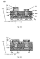
- Fig. 1(a) is a cross-sectional view showing an exemplary configuration of a nonvolatile semiconductor memory device 100.
- Fig. 1(b) is a cross-sectional view taken along one-dotted line of Fig. 1(a) .
- the nonvolatile semiconductor memory device 100 includes a substrate 102 provided with a transistor 101, a first interlayer insulating layer 103 formed over the substrate 102 to cover the transistor 101, a first contact plug 104 penetrating the first interlayer insulating layer 103 and electrically connected to either a drain electrode 101a or a source electrode 101b of the transistor 101, and a second contact plug 105 penetrating the first interlayer insulating layer 103 and electrically connected to the other of the drain electrode 101a or the source electrode 101b of the transistor 101.
- the nonvolatile semiconductor memory device 100 further includes resistance variable layer 106 covering the entire first contact plug 104, a first wire 107 formed on the resistance variable layer 106, and second wire 108 covering a portion of the second contact plug 105.
- the resistance variable layer 106 has end surfaces coplanar with the end surfaces of the first wire 107.
- the transistor 101 includes a first main electrode (drain electrode 101a), a second main electrode (source electrode 101b) and a control electrode (gate electrode 101e).
- the first main electrode is connected to the first contact plug 104, while the second main electrode is connected to the second contact plug 105.
- Which of the first main electrode and the second main electrode is the drain electrode or the source electrode is not particularly limited, but they may be reversed.
- the resistance variable layer 106 covers the entire upper end surface of the first contact plug 104 (this upper end surface is coplanar with the upper end surface of the interlayer insulating layer 103). Although it will be sufficient that the resistance variable layer 106 covers a portion of the upper end surface of the first contact plug 104, the resistance variable layer 106 desirably covers the entire upper end surface of the first contact plug 104.
- the first wire 107 includes an electrode layer 109 comprising at least precious metal on the surface contacting the resistance variable layer 106.
- the electrode layer 109 comprises, for example, platinum.
- an end surface including an end surfaces of the resistance variable layer 106 and the end surface of the first wire 107 is planarized.
- a drain region 101c is formed to underlie the drain electrode 101a, while a source region 101d is formed to underlie the source electrode 101b.
- a gate electrode 101e is formed between the drain electrode 101a and the source electrode 101b.
- a first contact hole 104a and a second contact hole 105a are formed to penetrate the first interlayer insulating layer 103 such that the first contact hole 104a is filled with the first contact plug 104, and the second contact hole 105a is filled with the second contact plug 105.
- a resistance variable element 111 includes an upper electrode consisting of the first wire 107 and the electrode layer 109, a lower electrode consisting of the first contact plug 104, and the resistance variable layer 106 sandwiched between the upper electrode and the lower electrode, and has a miniaturized structure at a bottom portion of the first wire 107.
- the resistance variable element 111 and the corresponding transistor 101 are coupled to each other in series, thereby forming a memory cell 112.
- the resistance variable layer 106 may comprise a material including at least tantalum oxide.
- nonvolatile semiconductor memory device 100 which has a reversible and stable rewrite characteristic and a good resistance value retention characteristic as well as high-speed operability and can be manufactured in a manufacturing process which is highly compatible with a standard Si semiconductor process.
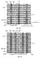
- Fig. 1(c) is a cross-sectional view showing a detail of an exemplary configuration of an array of the nonvolatile semiconductor memory device 100.
- Fig. 1(d) is a cross-sectional view taken along one-dotted line of Fig. 1(c) .
- the second wire 108 is connected to the third wire 115 via third contact 114 penetrating a second interlayer insulating layer 113 formed over the interlayer insulating layer 103.
- the first wire 107 crosses the third wire 115 perpendicularly to the third wire 115 when viewed in the thickness direction of the substrate 102.
- Fig. 1(e) is a plan view showing a detail of the exemplary configuration of the array of the nonvolatile semiconductor memory device 100.
- One gate electrode 101e of the transistor is shared by a plurality of elements, while the source region 101c and the drain region 101d are independently formed to respectively correspond to the elements.
- One first wire 107 is shared by a plurality of elements and one third wire 115 is shared by a plurality of elements.
- the electrode layer 109 and the resistance variable layer 106 which have a rectangular shape are formed on the first contact plug 104 individually formed.
- the second wire 108 is formed to cover the entire upper end surface of the second contact plug 105.
- the third contact plug 114 is formed on the second wire 108.
- the third wire 115 is formed to cover the entire upper end surfaces of the plurality of third contact plugs 114, respectively.
- the drain electrode 101b is electrically connected to the third wire 115 via the second contact plug 105, the second wire 108 and the third contact plug 114.
- the nonvolatile semiconductor memory device 100 includes the first wire 107 extending in parallel with each other in a first direction within a first plane parallel to a main surface of the substrate 102, and the third wire 115 extending in parallel with each other in a second direction three-dimensionally crossing the first direction within a second plane parallel to the first plane.
- the first wire 107 cross the third wire 115 perpendicularly to the third wire 115.
- the source electrode 101a are formed on the substrate in regions below the first wire 107.
- the drain electrode 101b is formed on the substrate in regions below the third wire 115, where the first wire 107 is not present.
- the gate electrode 101e is embedded in the interlayer insulating layer 103, between the source electrode 101a and the drain electrode 101b.
- the first wire 107 and the third wire 115 are electrically connected to the plurality of memory cells 112.
- the first contact plug 104 penetrating the interlayer insulating layer 103, the resistance variable layer 106 covering the entire upper end surface of the first contact plug 104, and the electrode layer 109 are stacked together in this order.
- the direction (rightward and leftward direction in Fig. 1(b) ) in which the first wire 107 extend is a forward and rearward direction (first direction)
- the direction (direction perpendicular to the drawing sheet in Fig. 1(b) ) which is perpendicular to the first direction and horizontal to the main surface of the substrate 102 is a rightward and leftward direction
- the direction perpendicular to the main surface of the substrate 102 upward and downward direction in Fig.
- FIG. 1 (b) is an upward and downward direction
- the end surfaces of the resistance variable layer 106 in the forward and rearward direction are covered with the first wire 107
- the end surfaces of the resistance variable layer 106 in the forward and rearward direction are not coplanar with the end surfaces of the first wires 107 in the forward and rearward direction
- the left end surface of the resistance variable layer 106 is coplanar with the left end surface of the first wire 107 as shown in Fig. 1(a)
- the right end surface of the resistance variable layer 106 is coplanar with the right end surface of the first wire 107 as shown in Fig. 1(a) .
- which one is called right or left may be arbitrary.
- the array has a feature that the plurality of resistance variable elements 111 are formed to underlie the first wires 107, which has an advantage in miniaturization.
- Fig. 1(f) is a plan view showing another exemplary configuration of the array of the nonvolatile semiconductor memory device 100.
- a threshold voltage required to change the resistance value of the resistance variable layer 106 is expressed as Vp.
- the voltage Vp is applied to the first wire 107, a voltage 2Vp which is twice as large as Vp is applied to the second wire 108, and a predetermined voltage for turning ON the transistor 101 is applied to the gate electrode 101e.
- the voltage 2Vp is applied to the first contact plug 104 which is the lower electrode of the resistance variable element 111 via the second contact plug 105 and the transistor 101.
- the resistance value of the resistance variable layer 106 changes, thereby allowing new data to be written to the resistance variable element 111.
- the voltage Vp is applied to the first wire 107, a voltage (Vp + ⁇ V) which is an intermediate value between the voltage Vp and the voltage 2Vp is applied to the second wire 108, and a predetermined voltage is applied to the gate electrode 101e to turn ON the transistor 101.
- the voltage ⁇ V which is lower than the threshold voltage Vp is applied to the resistance variable element 111.
- data of the resistance variable element 111 remain unchanged, and a current corresponding to the resistance value retained stably in the resistance variable element 111 flows through the resistance variable element 111. By reading this current, the data stored in the resistance variable element 111 can be read.
- the 1T1R-type memory cell 112 is formed.
- the lower electrode of the resistance variable element 111 and the first contact plug 104 are constituted by an identical constituent, while the upper electrode of the resistance variable element 111 and the first wire 107 are constituted by an identical constituent.
- the memory cell is allowed to have a simplified and miniaturized structure. Since the end surfaces of the resistance variable layer 106 are coplanar with the end surfaces of the first wire 107 (they are located on the same plane), the memory cell can be miniaturized without providing a margin allowing for alignment between different masks used to form the resistance variable layer 106 and the first wire 107 separately. Since the resistance variable layer 106 can be formed by adding one mask to a standard Si semiconductor process as described later, it is possible to implement a nonvolatile semiconductor memory device at a reduced process cost without increasing the number of process steps.
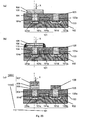
- Figs. 2(a) to 2(d) are cross-sectional views showing a manufacturing method of the nonvolatile semiconductor memory device 100.
- the manufacturing method includes a step of forming a first-interlayer insulating layer 103 over a substrate 102 provided with a transistor 101, a step of forming a first contact plug 104 and a second contact plug 105, a step of forming a resistance variable layer 106, a step of forming a first wire 107 and a step of forming a second wire 108.
- the first interlayer insulating layer 103 is formed over the substrate 102 provided with the transistor 101 to cover the transistor 101.
- a first contact hole 104a is formed on either a drain electrode 101a or a source electrode 101b of the transistor 101 to penetrate the first interlayer insulating layer 103
- the second contact hole 105a is formed on the other of the drain electrode 101 a or the source electrode 101b of the transistor 101 to penetrate the first interlayer insulating layer 103
- the first contact plug 104 and the second contact plug 105 are formed such that the first contact plug 104 is filled into the first contact hole 104a, and the second contact plug 105 is filled into the second contact hole 105a.
- the resistance variable layer 106 and the electrode layer 109 are formed to cover the entire opening of a first contact hole 104a.
- the electrode layer 109 precious metal material, for example, platinum layer may be used to enable the resistance variable layer 106 to operate well, i.e., easily change resistance.
- the resistance variable layer 106 and the electrode layer 109 are formed in such a manner that a resistance variable material and an electrode material are deposited over the entire upper surface of the interlayer insulating layer 103, a mask (photoresist or the like) having a predetermined shape is provided over the materials, and then etching is conducted using the mask.
- the first wire 107 and the second wire 108 are formed in such a manner that a wire material is deposited over the entire upper surface of the interlayer insulating layer 103 to cover the resistance variable layer 106 and the electrode layer 109, then a mask (photoresist or the like) having a predetermined shape is provided over the wire material, and then etching is conducted using the mask.
- the resistance variable layer 106 and the electrode layer 109 may be etched successively concurrently with the formation of the first wire 107, or the photoresist may be removed after forming the first wire 107, and then the resistance variable layer 106 and the electrode layer 109 may be etched using the first wire 107 as a mask.
- the first wire 107 and the second wire 108 may be formed simultaneously concurrently in the same step.
- the step for forming the first wire 107 is also the step for forming the second wire 108.
- electrode layer 109 may be omitted to make the manufacturing method simpler.
- a 1T1R-type memory cell 112 is formed, and the lower electrode of the resistance variable element 111 and the first contact plug 104 are constituted by an identical constituent, while the upper electrode of the resistance variable element 111 and the first wire 107 are constituted by an identical constituent, thereby resulting in a simplified and miniaturized structure of the memory cell 112.
- the resistance variable layer 106 can be formed by adding one mask to a standard Si semiconductor process, for example, a CMOS manufacturing process, it is possible to implement the nonvolatile semiconductor memory device 100 at a reduced process cost without increasing the number of process steps.
- the left end surface of the resistance variable layer is coplanar with the left end surface of the first wire and the right end surface of the resistance variable layer are coplanar with the right end surface of the first wire.
- the first wire or mask such as the photoresist for forming the first wire
- the number of required masks can be reduced.
- the resistance variable layer 106 is formed independently like the example of Fig. 15 , it is necessary to ensure adhesiveness of a photoresist to the resistance variable layer 106 to surely implement a square shape. Therefore, an element area must be set relatively larger.
- the resistance variable layer 106 is formed at regions where line-shaped resistance variable material and line-shaped wire material cross each other.
- the line-shaped resistance variable material can be set to have a smaller width than a square resistance variable material. As a result, the element area can be made smaller than that of the example of Fig. 15 .
- a precious metal layer for example, a platinum layer may be formed between the resistance variable layer 106 and the first wire 107.
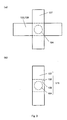
- Figs. 3(a) and 3(b) are plan views of enlarged major constituents of the nonvolatile semiconductor memory device 100 which are when viewed in the direction of arrow X of Figs. 2(c) and 2(d) .
- Fig. 3(a) shows a state where the first wire 107 is formed on the resistance variable layer 106 and the electrode layer 109 in the configuration of Fig. 2(c) but a portion of the resistance variable layer 106 and a portion of the electrode layer 109 which protrude outward to the right and to the left are not removed yet.
- the first wire 107 of a rectangular shape is formed on the resistance variable layer 106 and the electrode layer 109 of a rectangular shape covering the first contact plug 104 such that the first wire 107 crosses the resistance variable layer 106 and the electrode layer 109 perpendicularly to the resistance variable layer 106 and the electrode layer 109.
- the first wire 107 comprises a conductive material such as Al.
- the resistance variable layer 106 may comprise a material including at least tantalum oxide.
- an end surface of the resistance variable layer 106 is coplanar with an end surface of the first wire 107 (their end surfaces are on the same plane), these end surfaces may have unevenness depending on a variation in the shapes during manufacturing process steps (etching, etc).
- the first contact plug 104 is directly connected to the drain electrode 101a of the transistor, and the second contact plug 105 is directly connected to the source electrode 101b of the transistors, wire, contact plug or the like may intervene between the first contact plug 104 and the drain electrode 101a and between the second contact plug 105 and the source electrode 101b so long as electric connection is formed between them.
- Fig. 16(a) is a cross-sectional view showing an exemplary configuration of a nonvolatile semiconductor memory device 100A and Fig. 16(b) is a cross-sectional view taken along one-dotted line in the cross-sectional view of Fig. 16(a) .
- the electrode layer 109 has the same shape as the resistance variable layer 106 when viewed in the thickness direction of the substrate 102 (see Fig. 1(c) ).
- electrode layer 109' have the same shape as the first wire 107 when viewed in the thickness direction of the substrate 102 (see Fig. 16(b) ).
- the first wire 107 and the electrode layer 109' extend in a first direction, and the width (width in the rightward and leftward direction in a case where the first direction is a forward and rearward direction and a thickness direction of a substrate is an upward and downward direction) of the first wire 107 is equal to the width (width in the rightward and leftward direction) of the electrode layer 109'.
- the electrode layer 109 is isolated for each of the memory cells 112.
- the electrode layer 109' is shared by a plurality of memory cells 112. In such a configuration, flexibility of microfabrication of the electrode layer is improved and cells of further miniaturized configuration are easily formed in array.
- Figs. 17(a) to 17(d) are cross-sectional views showing a manufacturing method of the nonvolatile semiconductor memory device 100A. The difference between the manufacturing method of the nonvolatile semiconductor memory device 100 and the manufacturing method of the nonvolatile semiconductor memory device 100A will be described. Figs. 17(a) and 17(b) are similar to Figs. 2(a) and 2(b) , and therefore, will not be described in detail.
- Fig. 17(c) is a view showing a step of forming the resistance variable layer 106.
- the resistance variable layer 106 is formed to cover the entire opening of a first contact hole 104a (cover entire upper end surface of the first contact plug 104).
- the electrode layer 109 is not formed, but a resistance variable material is deposited over the entire surface of the interlayer insulating layer 103 and then etched using a desired mask, to form only the resistance variable layer 106.
- Fig. 17(d) is a view showing a step of forming the first wires 107 and the second wires 108.
- a step of forming the electrode layer 109' and the first wire 107 located thereabove which is also used as a mask for covering a portion of the resistance variable layer 106 to remove a remaining portion of the resistance variable layer 106, and a step of forming the electrode layer 109' and the second wire 108 located thereabove such that the electrode layer 109' and the second wire 108 cover a portion of the second contact plug 105, may be performed, thereby manufacturing the nonvolatile semiconductor memory device 100A.
- the electrode layer 109', the first wire 107 and the second wire 108 may be formed in such a manner that an electrode material and a wire material are deposited over the entire upper surface of the interlayer insulating layer 103 to cover the resistance variable layer 106, and etched using a mask (photoresist, or the like) of a predetermined shape.
- the resistance variable layer 106 may be etched successively concurrently with the formation of the first wire 107 and the electrode layer 109'.
- a photoresist may be removed, and the resistance variable layers 106 may be etched using the first wire 107 and the electrode layer 109' as a mask
- the first wire 107 and the second wire 108 may be formed simultaneously and concurrently in the same step.
- the step for forming the first wire 107 is also the step for forming the second wire 108.
- a problem such as disconnection tends to occur.
- the electrode layer 109 is required to be provided because of a problem such as an electrode material for enabling the resistance change, there is a level difference corresponding to a sum of the resistance variable layer 106 and the electrode layer 109 in the configuration of Fig. 1(b) , whereas there is a level difference corresponding to only the resistance variable layer 106 in the configuration of Fig. 17(d) .
- a focal depth in a lithography step associated with the first wire 107 and the second wire 108 can be improved, a process variation can be reduced, and further miniaturized wires can be formed.
- Figs. 18(a) and Fig. 18(b) are plan views of enlarged major constituents of the nonvolatile memory device 100A which are viewed taken in the direction of arrow X of Figs. 17(c) and 17(d) , respectively.
- Fig. 18(a) shows a state where the electrode layer 109' and the first wire 107 are formed on the resistance variable layer 106 in the configuration of Fig. 17(c) but a portion of the resistance variable layer 106 which protrudes outward to the right and to the left is not removed yet.
- the first wire 107 and the electrode layer 109' of a rectangular shape are formed to cross the resistance variable layer 106 perpendicularly to the resistance variable layer 106.
- the first wire 107 comprises a conductive material such as AI. Using the first wire 107 as a mask, an unnecessary portion of the resistance variable layer 106 is removed, thereby manufacturing the resistance variable element 111A having a miniaturized structure as shown in Fig. 18(b) .
- Fig. 19(a) is a cross-sectional view showing an exemplary configuration of a nonvolatile semiconductor memory device 100B
- Fig. 19(b) is a cross-sectional view taken along one-dotted line in the cross-sectional view of Fig. 19(a) .
- the electrode layer 109 has the same shape as the resistance variable layer 106 when viewed in the thickness direction of the substrate 102 (see Fig. 1(c) ).
- electrode layer 109" is filled on filling layer 104' (inside the first contact hole 104a). The electrode layer 109" and the filling layer 104' constitute first contact plug.
- the filling layer 104' may be formed using the same material and the same method as those for the first contact plug 104 except that the upper end surface of the filling layer 104' is accommodated inside the first contact hole 104a (lower than the upper end surface of the interlayer insulating layer 103).
- Figs. 20(a) to 20(d) are cross-sectional views showing a manufacturing method of the nonvolatile semiconductor memory device 100B. The difference between the manufacturing method of the nonvolatile semiconductor memory device 100B and the manufacturing method of the nonvolatile semiconductor memory device 100 will be described.
- Figs. 20(a), 20(c), and 20(d) are similar to Figs. 2(a), 2(c), and 2(d) , and will not be described in detail.
- recesses are formed at the upper portion of the first contact plug 104 and the upper portion of the second contact plug 105, by, for example, etch back, to form the filling layers 104' and 105'.
- An electrode material is deposited to completely fill the recesses on the filling layers 104' and 105'.
- electrode material on the first interlayer insulating layer 103 is removed to form the electrode layer 109" filled into the recesses, respectively.
- the filling layer 104' and the electrode layer 109" constitute the first contact plug.
- the filling layer 105' and the electrode layer 109" constitute the second contact plug.
- the resistance variable layer 106 covers the entire upper end surface of the first contact plug(upper end surface of the electrode layer 109") .
- a "contact plug” is defmed as a conductor filled into a contact hole.
- the contact plug may have a single layer or a plurality of layers.
- the upper end surface of the contact plug serves as the lower electrode of the resistance variable element.
- the manufacturing method has an advantage that flexibility of microfabrication of the electrode layer is improved and cells of further miniaturized configuration are easily formed.
- Figs. 21(a) and Fig. 21(b) are plan views of enlarged major constituents of the nonvolatile memory device 100B which are viewed taken in the direction of arrow X of Figs. 20(c) and 20(d) , respectively.
- Fig. 21 (a) shows a state where the first wire 107 is formed on the resistance variable layer 106 in the configuration of Fig. 17(c) but a portion of the resistance variable layer 106 which protrudes outward to the right and to the left is not removed yet.
- the first wire 107 of a rectangular shape is formed on the resistance variable layer 106 of a rectangular shape covering the first contact plug (electrode layer 109") to cross the resistance variable layer 106 perpendicularly to the resistance variable layer 106.
- the first wire 107 comprise a conductive material such as A1.
- Fig. 22(a) is a cross-sectional view showing an exemplary configuration of a nonvolatile semiconductor memory device 100C
- Fig. 22(b) is a cross-sectional view taken along one-dotted line in the cross-sectional view of Fig. 22(a) .
- side wall insulating layer 113 is formed on the side walls of the electrode layer 109 and the side walls of the resistance variable layer 106 (end surfaces of the electrode layer 109 and end surfaces of the resistance variable layer 106 in the forward and rearward direction).
- the nonvolatile semiconductor memory device 100C because of the side wall insulating layer 113, steps between the electrode layer 109 and the resistance variable layer 106 are lessened and the first wire 107' is less likely to be disconnected at the steps. In addition, a variation in wire resistance of the first wire 107' can be reduced.
- Figs. 23(a) to 23(c) and Figs. 24(a) to 24(c) are cross-sectional views showing a manufacturing method of the nonvolatile semiconductor memory device 100C.
- Figs. 24(a), 24(b) and 24(c) are cross-sectional views taken along one-dotted lines of the cross-sectional views of Figs. 23(a), 23(b) and 23(c) , respectively.
- Figs. 23(a) and 24(a) are views showing steps of forming the electrode layer 109 and the resistance variable layer 106.
- the resistance variable layer 106 and the electrode layer 109 are formed to cover entire opening of first contact hole 104a (cover entire upper end surface of the first contact plug 104).
- Fig. 23(b) and 24(b) are views showing a step of forming the side wall insulating layer 113.
- an insulating layer is formed over the entire upper surface of the interlayer insulating layer 103 to cover the entire electrode layer 109 and the entire resistance variable layer 106, and the entire surface of the insulating layer is etched back, thereby forming the side wall insulating layer 113 on the side walls at the steps formed by the electrode layer 109 and the resistance variable layer 106.
- Figs. 23(c) and 24(c) are views showing the step of forming the first wire 107' and the second wire 108.
- a step of forming the first wire 107' which is also used as a mask for covering a portion of the resistance variable layer 106, a portion of the electrode layer 109, and a portion of the side wall insulating layer 113 to remove a remaining portion of the resistance variable layer 106, a remaining portion of the electrode layer 109 and a remaining portion of the side wall insulating layer 113, and a step of covering a portion of the second contact plug 105 to form the second wire 108, is performed, thereby manufacturing the nonvolatile semiconductor memory device 100C.
- the first wire 107' and the second wire 108 are formed in such a manner that a wire material is deposited over the entire upper surface of the interlayer insulating layer 103 to cover the resistance variable layer 106 and the electrode layer 109, a mask (photoresist or the like) having a predetermined shape is provided over the wire material, and then etching is conducted using the mask.
- the resistance variable layer 106 and the electrode layer 109 may be etched successively concurrently with the formation of the first wire 107.'
- the photoresist may be removed after forming the first wire 107', and then the resistance variable layer 106 and the electrode layer 109 may be etched using the first wire 107' as a mask.
- the first wire 107' and the second wire 108 may be formed simultaneously concurrently in the same step.
- the step for forming the first wire 107' is also the step for forming the second wire 108.
- the first wire 107' is less likely to be disconnected at the steps in a lithography step for forming the first wire 107' and the second wire 108.
- a variation in wire resistance of the first wire 107' can be reduced.
- Figs. 25(a) and Fig. 25(b) are plan views of enlarged major constituents of the nonvolatile memory device 100C which are viewed taken in the direction of arrow X of Figs. 23(c) and 23(d) , respectively.
- Fig. 25(a) shows a state where the first wire 107' is formed on the resistance variable layer 106 and the electrode layer 109 in the configuration of Fig. 23(b) but a portion of the resistance variable layer 106 and a portion of the electrode layer 109 which protrude outward to the right and to the left are not removed yet.
- the first wire 107' of a rectangular shape is formed on the resistance variable layer 106 and the electrode layer 109 of a rectangular shape covering the first contact plug 104 such that the first wire 107' crosses the resistance variable layer 106 and the electrode layer 109 perpendicularly to the resistance variable layer 106 and the electrode layer 109.
- the first wire 107' comprises a conductive material such as Al.
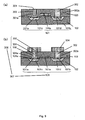
- Fig. 4 is a cross-sectional view showing an exemplary configuration of a nonvolatile semiconductor memory device 200 according to an embodiment of the present invention.
- the nonvolatile semiconductor memory device 200 of the embodiment includes a substrate 102 provided with a transistor 101, a first interlayer insulating layer 103 formed on the substrate 102 to cover the transistor 101, a first contact plug 104 penetrating the first interlayer insulating layer 103 and electrically connected to either a drain electrode 101a or a source electrode 101b of the transistor 101, and a second contact plug 105 penetrating the first interlayer insulating layer 103 and electrically connected to the other of the drain electrode 101a or the source electrode 101b of the transistor 101.
- the nonvolatile semiconductor memory device 200 further includes a first wire 201 covering a portion of the first contact plug 104, a first resistance variable layer 202 formed on the first wire 201 to have the same shape as the first wire 201, a second wire 203 covering a portion of a second contact plug 105, a second resistance variable layer 204 formed on the second wire 203 to have the same shape as the second wire 203, and a second interlayer insulating layer 205 formed over the first interlayer insulating layer 103 to cover the first wire 201 and the second wire 203.
- the nonvolatile semiconductor memory device 200 includes a third contact plug 206 formed on the first resistance variable layer 202 to penetrate the second interlayer insulating layer 205, a fourth contact plug 207 formed on the second wire 203 to penetrate the second interlayer insulating layer 205 and the second resistance variable layer 204, a third wire 208 formed on the second interlayer insulating layer 205 to cover the third contact plug 206, and a fourth wire 209 formed on the second interlayer insulating layer 205 to cover the fourth contact plug 207.
- a resistance variable element 210 includes the first wire 201 which is the lower electrode, the first resistance variable layer 202 and the third contact plug 206 which is the upper electrode.
- a 1T1R-type memory cell 211 is formed, and the lower electrode of the resistance variable element 210 and the first wire 201 are constituted by an identical constituent, while the upper electrode of the resistance variable element 210 and the third contact plug 206 are constituted by an identical constituent, thereby resulting in a simplified and miniaturized structure of the memory cell 211.
- nonvolatile semiconductor memory device 200 operates similarly to the nonvolatile semiconductor memory device 100 described, the operation example will not be described repetitively.
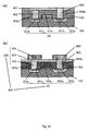
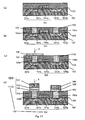
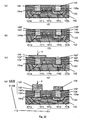
- Figs. 5(a) to 5(c) and Figs. 6(a) and 6(b) are cross-sectional views showing a manufacturing method of the nonvolatile semiconductor memory device 200.
- the manufacturing method of the nonvolatile semiconductor memory device 200 will be described with reference to Figs. 5(a) to 5(c) and Figs. 6(a) and 6(b) .
- the manufacturing method includes a step of forming the first interlayer insulating layer 103 over the substrate 102 provided with the transistor 101, a step of forming the first contact plug 104 and the second contact plug 105, a step of forming the first wire layer and the resistance variable layer, a step of forming the first wire 201, the second wire 203, the first resistance variable layer 202 and the second resistance variable layer 204 such that the first resistance variable layer 202 has the same shape as the first wire 201 and the second resistance variable layer 204 has the same shape as the second wire 203, a step of forming the second interlayer insulating layer 205, a step of forming the third contact plug 206, a step of forming the fourth contact plug 207 and a step of forming the third wire 208 and the fourth wire 209.
- the first interlayer insulating layer 103 is formed over the substrate 102 to cover the transistor 101.
- a first contact hole 104a is formed on either a drain electrode 101a or a source electrode 101b of the transistor 101 to penetrate the first interlayer insulating layer 103
- a second contact hole 105a is formed on the other of the drain electrode 101a or the source electrode 101b of the transistor 101 to penetrate the first interlayer insulating layer 103
- a conductor is filled into the first contact hole 104a and the second contact hole 105a to form the first contact plug 104 and the second contact plug 105, respectively.
- thin layers which will become the first wire layer and the resistance variable layer are deposited over the first interlayer insulating layer 103 to cover the first contact plug 104 and the second contact plug 105.
- the first wire 201 and the first resistance variable layer 202 are formed on the first contact plug 104 and the second wire 203 and the second resistance variable layer 204 are formed on the second contact plug 105 such that the first wire 201 and the first resistance variable layer 202 are isolated from the second wire 203 and the second resistance variable layer 204.
- the second interlayer insulating layer 205 is formed over the first interlayer insulating layer 103 to cover the first wire 201, the first resistance variable layer 202, the second wire 203 and the second resistance variable layer 204.
- Fig. 6(b) shows a step of forming the third contact plug 206, a step of forming the fourth contact plug 207, and a step of forming the third wire 208 and the fourth wire 209.
- a third contact hole 206a is formed on the first resistance variable layer 202 to penetrate the second interlayer insulating layer 205.
- a fourth contact hole 207a is formed on the second wire 203 to penetrate the second interlayer insulating layer 205 and the second resistance variable layer 204.
- a hole penetrating a part of the second resistance variable layer 204 is formed in such a manner that the fourth contact hole 207a is formed to reach the second resistance variable layer 204 concurrently with the formation of the third contact hole 206a reaching the first resistance variable layer 202, and then the hole is formed using the fourth contact hole 207a as an open mask.
- a conductor material is filled into the third contact hole 206a to form the third contact plug 206, and into the fourth contact hole 207a, to form the fourth contact plug 207.
- the third wire 208 is formed on the second interlayer insulating layer 205 to cover the third contact plug 206
- the fourth wire 209 is formed on the second interlayer insulating layer 205 to cover the fourth contact plug 207 such that the third wire 208 is isolated from the fourth wire 209.
- the nonvolatile semiconductor memory device 200 is manufactured to include a 1 T1R memory cell 211 including the resistance variable element 210 and the transistor 101.
- the first wire 201 which is a wire of the memory cell 211
- the second wire 203 which is also used as a wire connected with a memory driving section or a peripheral circuit can be formed concurrently in the same step, which results in simplified process steps.
- the resistance variable element 210 includes the first wire 201 which is the lower electrode, the third contact plug 206 which is the upper electrode, and the first resistance variable layer 202 sandwiched between the first wire 201 and the third contact plug 206.
- the memory cell 211 has a simplified and miniaturized structure.
- the resistance variable layer can be formed by adding only one mask for forming a hole to a standard Si semiconductor process, the number of process steps does not increase. This enables high-dense integration, higher speed, and lower electric power consumption. In addition, the manufacturing process steps are simplified and as a result, a manufacturing time period and a manufacturing cost can be reduced.
- the third contact hole 206a and the fourth contact hole 207a which are different in depth can be formed concurrently, by making use of a feature of a hole etching that an etching rate is higher as the size is larger. In this case, it is possible to implement a nonvolatile semiconductor memory device at a lower process cost without adding any masks.
- the first resistance variable layer 202 may comprise a material including at least tantalum oxide.
- the first contact plug 104 is directly connected to the drain electrode 101 a of the transistors
- the second contact plug 105 is directly connected to the source electrode 101b of the transistors, respectively, wires, contact plugs or the like may intervene between the first contact plug 104 and the drain electrode 101b and between the second contact plug 105 and the source electrode 101b so long as electric connection is formed between them.
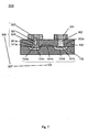
- Fig. 7 is a cross-sectional view showing an exemplary configuration of a nonvolatile semiconductor memory device 300.
- the nonvolatile semiconductor memory device 300 includes a substrate 102 provided with a transistor 101, a first interlayer insulating layer 103 formed on the substrate 102 to cover the transistor 101, a first contact plug 301 penetrating the first interlayer insulating layer 103 and electrically connected to either a drain electrode 101a or a source electrode 101b of the transistor 101, and second contact plug 302 penetrating the first interlayer insulating layer 103 and electrically connected to the other of the drain electrode 101a or the source electrode 101b of the transistor 101.
- the nonvolatile semiconductor memory device 300 includes first wire 303 covering a portion of the first contact plug 301, second wire 304 covering a portion of the second contact plug 302, and resistance variable layer 305 formed on a bottom portion and a side wall inside the first contact hole 301a such that the resistance variable layer 305 is sandwiched between the first contact plug 301, and the first interlayer insulating layer 103 and the drain electrode 101a or between the first contact plug 301, and the first interlayer insulating layer 103 and the source electrode 101b.
- the nonvolatile semiconductor memory device 300 is manufactured to include a 1T1R-type memory cell 307 including the resistance variable element 306 and the transistor 101.
- the first wire 303 which is the wire of the memory cell 307 and the second wire 304 which may also be used as the wire connected with the memory driving section or the peripheral circuit can be formed concurrently in the same step, the process steps are simplified.
- a resistance variable element 306 includes the drain electrode 101a which is the lower electrode, the first contact plug 301 and the first wire 303 which are the upper electrode, and the resistance variable layer 305 sandwiched between the drain electrode 101a, and the first contact plug 301 and the first wire 303
- the memory cell 307 has a simplified and miniaturized structure. Since the bottom portion of the resistance variable layer 305 is not exposed during processes such as CMP or dry etching, plasma damage, damage caused by gases or slurry, influence of reduction, etc. with respect to the resistance variable layer 305 can be surely prevented.
- the resistance variable layer 305 which is formed to be miniaturized and integrated in contact with the bottom portion and the side wall inside the first contact hole 301 a, can be formed by adding only one mask to the standard Si semiconductor process. Therefore, the number of the manufacturing process steps of the nonvolatile semiconductor memory device 300 does not increase. This enables the nonvolatile semiconductor memory device 300 to achieve further miniaturization, high-dense integration, higher speed, and lower electric power consumption. In addition, the manufacturing process steps are simplified and as a result, a manufacturing time period and a manufacturing cost can be reduced.
- nonvolatile semiconductor memory device 300 operates similarly to the nonvolatile semiconductor memory device 100, the operation example will not be described repetitively.
- Figs. 8(a) to 8(c) and Figs. 9(a) and 9(b) are cross-sectional views showing a manufacturing method of the nonvolatile semiconductor memory device 300.
- the manufacturing method of the nonvolatile semiconductor memory device 300 will be described with reference to Figs. 8(a) to 8(c) and Figs. 9(a) and 9(b) .
- the manufacturing method of Embodiment 3 includes a step of forming the first interlayer insulating layer 103 over the substrate 102 provided with the transistor 101, a step of forming the resistance variable layer 305 and the first contact plug 301 inside the first contact hole,, a step of forming the second contact plug 302, and a step of forming the first wire layer 303 and the second wire 304.
- the first interlayer insulating layer 103 is formed over the substrate 102 to cover the transistor 101.
- first contact hole 301a is formed on the drain electrode 101a of the transistor 101 to penetrate the first interlayer insulating layer 103, then a resistance variable layer is deposited over the entire surface, and a portion of the resistance variable layer on the first interlayer insulating layer 103 is removed by CMP or etching, thereby forming the resistance variable layer 305 on a bottom portion and a side wall of the first contact hole 301a.
- a conductor is filled into inside the first contact hole 301a and the resistance variable layer 305, to form the first contact plug 301.
- the first contact hole 302a is formed on the source electrode 101b of the transistor 101 to penetrate the first interlayer insulating layer 103, and a conductor is filled into the first contact hole 302a, to form the second contact plug 302.
- Fig. 9(b) shows a step of forming the first wire 303 and the second wire 304.
- the first wire 303 is formed to cover a portion of the resistance variable layer 305 and a portion of the first contact plug 301
- the second wire 304 are formed to cover a portion of the second contact plug 302 such that the first wire 303 is isolated from the second wire 304.
- a 1T1R-type memory cell is formed, and the lower electrode of the resistance variable element and the drain electrode 101a are constituted by an identical constituent, while the upper electrode of each of the resistance variable elements is identical in constituent to the first wire 303 and the first contact plug 301, thereby resulting in a simplified and miniaturized structure of the memory cells.
- the resistance variable layer can be formed by adding only one mask to the standard Si semiconductor process, it is possible to implement a nonvolatile semiconductor memory device which does not increase the number of process steps and can reduce a process cost.
- the resistance variable element 306 includes the drain electrode 101a which is the lower electrode, the first wire 303 and the first contact plug 301 which are the upper electrode, and the resistance variable layer 305 sandwiched between the drain electrode 101 a, and the first wire 303 and the first contact plug 301.
- the memory cell 307 has a simplified and miniaturized structure. Since the resistance variable layer can be formed by adding only one mask to the standard Si semiconductor process, the number of process steps does not increase. This enables the nonvolatile semiconductor memory device 300 to achieve further miniaturization, high-dense integration, higher speed, and lower electric power consumption. In addition, the manufacturing process steps can be simplified, and a manufacturing time period and a manufacturing cost can be reduced.
- the resistance variable layer 305 may comprise a material including at least tantalum oxide.
- the resistance variable layer 305 is directly connected to the drain electrode 101a of the transistor, and the second contact plug 302 is directly connected to the source electrode 101b of the transistor, wires, contact plugs or the like may intervene between the resistance variable layer 305 and the drain electrode 101a and between the second contact plug 302 and the source electrode 101b so long as electric connection is formed between them.
- Fig. 10 is a cross-sectional view showing an exemplary configuration of a nonvolatile semiconductor memory device 400.
- the nonvolatile semiconductor memory device 400 includes a substrate 102 provided with a transistor 101, a first interlayer insulating layer 103 formed on the substrate 102 to cover the transistor 101, a resistance variable layer 401 formed over the first interlayer insulating layer 103, and a first contact plug 402 penetrating the first interlayer insulating layer 103 and electrically connected to either a drain electrode 101a or the source electrode 101b of the transistor 101.
- the nonvolatile semiconductor memory device 400 includes a second contact plug 403 penetrating the first interlayer insulating layer 103 and the resistance variable layer 401 and electrically connected to the other of the source electrode 101b or the drain electrode 101a of the transistor 101, a first wire 404 covering a portion of the resistance variable layer 401 on the first contact plug 402 and second wire 405 covering a portion of the second contact plug 403.
- the second contact plug 403 penetrate the resistance variable layer 401 and the first interlayer insulating layer 103, and is connected to the second wire 405.
- the resistance variable layer 401 is formed on the first interlayer insulating layer 103 to cover the first contact plug 402 and the second contact plug 403, and a portion of the resistance variable layer 401 on the second contact plug 403 are removed to form through-hole in the resistance variable layer 401. Then, a plug electrode material is filled into the through-hole and planarized, and then the first wire 404 and the second wire 405 are formed on the planarized surface such that the first wire 404 is isolated from the second wire 405, thereby manufacturing the nonvolatile semiconductor memory device 400.
- the resistance variable element 406 includes the first wire 404 which is the upper electrode, the first contact plug 402 which is the lower electrode, and the resistance variable layer 401 sandwiched between the upper electrode and the lower electrode.
- the memory cell 407 has 1T1R structure consisting of the resistance variable element 406 and the transistor 101.
- the lower electrode of the resistance variable element 406 and the first contact plug 402 are constituted by an identical constituent and the upper electrode of the resistance variable element 406 and the first wire 404 are constituted by an identical constituent, thereby allowing the memory cell 407 to have a simplified and miniaturized structure.
- the resistance variable element 406 is formed in a region where the first contact plug 402 does not penetrate the resistance variable layer 401. Since the resistance variable layer 401 is formed on a flat portion, it is sufficient that only a variation at the time of layer forming is taken into account, and a variation in cell resistances can be reduced.
- the resistance variable layer 401 can be surely prevented. Further, since the resistance variable layer 401 can be formed by adding only one mask to a standard Si semiconductor process, it is possible to implement the nonvolatile semiconductor memory device 400 which does not increase the number of process steps and can reduce a process cost.
- the manufacturing process steps are simplified and as a result, a manufacturing time period and a manufacturing cost can be reduced.
- nonvolatile semiconductor memory device 400 operates similarly to the nonvolatile semiconductor memory device 100, the operation example will not be described repetitively.
- Figs. 11(a) to 11(c) and Figs. 12(a) and 12(b) are cross-sectional views showing a manufacturing method of the nonvolatile semiconductor memory device 400.
- the manufacturing method of the nonvolatile semiconductor memory device 400 of Embodiment 4 will be described with reference to Figs. 11(a) to 11(c) and Figs. 12(a) and 12(b) .
- the manufacturing method includes a step of forming the first interlayer insulating layer 103 over the substrate 102 provided with the transistor 101, a step of forming the first contact plug 402, a step of forming the resistance variable layer 401, a step of forming the second contact plug 403, and a step of forming the first wire layer 404 and the second wire layer 405.
- the first interlayer insulating layer 103 is formed over the substrate 102 to cover the transistor 101.
- first contact hole 402a is formed on the drain electrode 101a of the transistor 101 to penetrate the first interlayer insulating layer 103, and then a conductor is filled into the first contact hole 402a, to form the first contact plug 402.
- the resistance variable layer 401 are deposited on the first interlayer insulating layer 103 to cover the first contact plug 402.
- second contact hole 403a is formed on the source electrode 101b of the transistor 101 to penetrate the resistance variable layers 401 and the first interlayer insulating layer 103, and then a conductor is filled into the second contact hole 403a, to form the second contact plug 403.
- Fig. 12(b) shows a step of forming the first wire 404 and the second wire 405.
- the first wire 404 is formed to cover a portion of the first contact plug 402
- the second wire 405 is formed to cover a portion of the second contact plug 403 such that the first wire 404 is isolated from the second wire 405.
- the nonvolatile semiconductor memory device 400 is manufactured to include the 1T1R-type memory cell 407 including the resistance variable element 406 and the transistor 101.
- the resistance variable element 407 includes the first contact plug 402 which is the lower electrode, the first wire 404 which is the upper electrode, and the resistance variable layer 401 sandwiched between the first contact plug 402 and the first wire 404, thereby allowing the memory cell 407 to have a simplified and miniaturized structure. Since the resistance variable layer can be formed by adding only one mask to the standard Si semiconductor process, the number of process steps does not increase. This enables the nonvolatile semiconductor memory device 400 to achieve further miniaturization, high-dense integration, higher speed, and lower electric power consumption. In addition, the manufacturing process steps can be simplified, and a manufacturing time period and a manufacturing cost can be reduced.
- the first resistance variable layer 401 may comprise a material including at least tantalum oxide.
- the first contact plug 402 is directly connected to the drain electrode 101 a of the transistor, and the second contact plug 403 is directly connected to the source electrode 101b of the transistor, wires, contact plugs or the like may intervene between the first contact plug 402 and the drain electrode 101a and between the second contact plug 403 and the source electrode 101b so long as electric connection is formed between them.
- Fig. 13 is a block diagram showing a configuration of a nonvolatile semiconductor device 500.
- Fig. 14 is an enlarged cross-sectional view showing a configuration (configuration corresponding to 2 bits) in part C of Fig. 13 .
- the nonvolatile semiconductor device 500 is a nonvolatile semiconductor device 500 including, for example, the nonvolatile semiconductor memory device 100, which includes a memory array including a plurality of word lines formed in, for example, a stripe shape on a substrate to extend in parallel with each other, a plurality of bit lines formed in a stripe shape in the same manner above the plurality of word lines within a plane parallel to a main surface of the substrate such that the plurality of bit lines three-dimensionally cross the word lines, and resistance variable elements provided to respectively correspond to three-dimensional cross-points of the plurality of word lines and the plurality of bit lines.
- the nonvolatile semiconductor memory device 100 which includes a memory array including a plurality of word lines formed in, for example, a stripe shape on a substrate to extend in parallel with each other, a plurality of bit lines formed in a stripe shape in the same manner above the plurality of word lines within a plane parallel to a main surface of the substrate such that the plurality of bit lines three-dimensionally
- the nonvolatile semiconductor device 500 includes a memory main section 501 on a semiconductor substrate.
- the memory main section 501 includes a memory array 502, a row select circuit/driver 503, a column select circuit 504, a write circuit 505 for writing data, a sense amplifier 506 which detects an amount of a current flowing through a selected bit line and determines the data, and a data input/output circuit 507 which executes input/output processing of input/output data via a terminal DQ.
- the memory array 502 includes a plurality of word lines WL0, WL1, WL2 and a plurality of bit lines BL0, BL1, BL2 which are formed on the substrate such that the plurality of word lines WL0, WL1, WL2 cross the plurality of bit lines BL0, BL1, BL2, a plurality of transistors T11, T12, T13, T21, T22, T23, T31, T32, T33 (hereinafter expressed as "transistors T11, T12, ") provided to respectively correspond to cross-points of the plurality of word lines WL0, WL1, WL2 and the plurality of bit lines BL0, BL1, BL2 and a plurality of resistance variable elements M11, M12, M13, M21, M22, M23, M31, M32, M33 (hereinafter referred to as "resistance variable elements M11, M12, ") provided to have a one-to-one relationship with the transistors T11,
- the memory array 502 further includes a plurality of plate lines PL0, PL1, and PL2 arranged to extend in parallel with the word lines WLO, WL1, and WL2.
- bit line BL0 is provided above the word lines WL0 and WL1
- the plate lines PL0 and PL1 are provided between the word lines WL0 and WL1 and the bit line BL0.
- the resistance variable element M11 of Fig. 13 corresponds to the resistance variable element M11 of Fig. 14 .
- the resistance variable element M11 includes the first wire 515 which is the upper electrode, the electrode layer 514 comprising precious metal, platinum, the resistance variable layer 513 and the first contact plug 511 which is the lower electrode.
- each of the memory cell 516 includes the transistor 101 and the resistance variable element M11.
- the transistor 101 is electrically connected to the bit line BL0 via a second contact plug 517, a second wire 518 and a third contact plug 519.
- Address signals are received from an external circuit (not shown), and row address signals and column address signals are output to the row select circuit/driver 503 and output to the column select circuit 504, respectively, based on the address signals.
- the address signals are signals indicating the address of a specified memory cell 516 to be selected from among memory cells 516 including the plurality of resistance variable elements M11, M12, ....
- the row address signals are signals indicating a row address in the address indicated by the address signals
- the column address signals are signals indicating a column address in the address indicated by the address signals.
- write signals for causing application of write voltages are output to the write circuit 505, according to the input data Din input to the data input/output circuit 507.
- read signal for causing application of read voltages is output to the column select circuit 504.
- the row select circuit/driver 503 receives the row address signals output from the address signals, select one from among the plurality of word lines WL0, WL1, WL2 based on the row address signals and applies a predetermined voltage to the selected word line.
- the column select circuit/driver 504 receives column address signals output from the address signals, selects one from among the plurality of bit lines BL0, BL1, BL2 based on the column address signals and applies the write voltage or the read voltage to the selected bit line.
- the write circuit 505 When the control signal is a write signal, the write circuit 505 outputs to the column select circuit 504 a signal for causing application of a write voltage to the selected bit line.
- the sense amplifier 506 detects an amount of a current flowing through the selected bit line which is a read target, and determines the data as "1" or "0.”
- the resulting output data DO is output to the external circuit via the data input/output circuit 507.
- a nonvolatile semiconductor memory device of the present invention is highly integrated, achieves lower electric power consumption and a high-speed operation, and has a stable write and read characteristic.
- the nonvolatile semiconductor memory device is useful as a nonvolatile semiconductor memory device for use with various electronic hardwares such as digital home appliance, memory cards, cellular phones, and personal computers.
Landscapes
- Engineering & Computer Science (AREA)
- Manufacturing & Machinery (AREA)
- Chemical & Material Sciences (AREA)
- Materials Engineering (AREA)
- Semiconductor Memories (AREA)
Claims (3)
- Dispositif de mémoire semi-conductrice non volatile comprenant :un substrat muni d'un transistor ;une première couche isolante intercalaire (103) formée sur le substrat pour couvrir le transistor ;une première fiche de contact (104) formée dans la première couche isolante intercalaire et électriquement connectée soit à une électrode drain soit à une électrode source du transistor, et une deuxième fiche de contact (105) formée dans la première couche isolante intercalaire et électriquement connectée à l'autre de l'électrode drain ou de l'électrode source du transistor ;un premier fil (107, 201) formé pour couvrir une partie de la première fiche de contact ;une première couche à résistance variable (106, 202) formée directement sur le premier fil pour avoir une surface terminale qui se trouve dans le même plan qu'une surface terminale du deuxième fil ;un deuxième fil (108, 203) formé pour couvrir une partie de la deuxième fiche de contact ;une seconde couche à résistance variable (204) formée directement sur le deuxième fil, pour avoir une surface terminale qui se trouve dans le même plan qu'une surface terminale du deuxième fil ;une seconde couche isolante intercalaire (113, 205) formée par-dessus la première couche isolante intercalaire pour couvrir le premier fil, le deuxième fil, la première couche à résistance variable et la seconde couche à résistance variable ;une troisième fiche de contact (114, 206) formée sur la première couche à résistance variable pour pénétrer la seconde couche isolante intercalaire ;une quatrième fiche de contact (207) formée sur le deuxième fil pour pénétrer la seconde couche isolante intercalaire et la seconde couche à résistance variable ; etun troisième fil (115, 208) et un quatrième fil (209) qui sont formés sur la seconde couche isolante intercalaire de sorte que le troisième fil couvre la troisième fiche de contact, et le quatrième fil couvre la quatrième fiche de contact.
- Dispositif de mémoire semi-conductrice non volatile selon la revendication 1, dans lequel la couche à résistance variable comprend un matériau incluant au moins de l'oxyde de tantale.
- Procédé de fabrication d'un dispositif de mémoire semi-conductrice non volatile comprenant les étapes de :former une première couche isolante intercalaire par-dessus un substrat muni d'un transistor de sorte que la première couche isolante intercalaire couvre le transistor ;former une première fenêtre de contact soit sur une électrode drain soit sur une électrode source du transistor et une seconde fenêtre de contact sur l'autre de l'électrode drain ou de l'électrode source du transistor de sorte que la première fenêtre de contact et la seconde fenêtre de contact pénètrent la première couche isolante intercalaire, et former une première fiche de contact dans la première fenêtre de contact et une deuxième fiche de contact dans la seconde fenêtre de contact ;former une première couche à résistance variable directement sur la première couche de fils de sorte que la première couche de fils et la première couche à résistance variable couvrent une partie de la première fiche de contact et la première couche à résistance variable a une surface terminale dans le même plan qu'une surface terminale de la première couche de fils, et former une seconde couche à résistance variable directement sur une seconde couche de fils de sorte que la seconde couche de fils et la seconde couche à résistance variable couvrent une partie de la deuxième fiche de contact et la seconde couche à résistance variable a une surface terminale dans le même plan qu'une surface terminale de la seconde couche de fils ;former une seconde couche isolante intercalaire par-dessus la première couche isolante intercalaire de sorte que la seconde couche isolante intercalaire couvre le premier fil, la première couche à résistance variable, le deuxième fil et la seconde couche à résistance variable ;former une troisième fiche de contact sur la première couche à résistance variable de sorte que la troisième fiche de contact pénètre la seconde couche isolante intercalaire ;former une quatrième fiche de contact sur le deuxième fil, de sorte que la quatrième fiche de contact pénètre la seconde couche isolante intercalaire et la seconde couche à résistance variable ; etformer un troisième fil et un quatrième fil sur la seconde couche isolante intercalaire de sorte que le troisième fil couvre la troisième fiche de contact et le quatrième fil couvre la quatrième fiche de contact.
Applications Claiming Priority (2)
| Application Number | Priority Date | Filing Date | Title |
|---|---|---|---|
| JP2008030242 | 2008-02-12 | ||
| EP09710369A EP2244293A4 (fr) | 2008-02-12 | 2009-02-09 | Dispositif de mémoire non volatile à semi-conducteur et son procédé de fabrication |
Related Parent Applications (2)
| Application Number | Title | Priority Date | Filing Date |
|---|---|---|---|
| EP09710369.1 Division | 2009-02-09 | ||
| EP09710369A Division EP2244293A4 (fr) | 2008-02-12 | 2009-02-09 | Dispositif de mémoire non volatile à semi-conducteur et son procédé de fabrication |
Publications (3)
| Publication Number | Publication Date |
|---|---|
| EP2447996A2 EP2447996A2 (fr) | 2012-05-02 |
| EP2447996A3 EP2447996A3 (fr) | 2013-02-06 |
| EP2447996B1 true EP2447996B1 (fr) | 2014-04-02 |
Family
ID=40956819
Family Applications (2)
| Application Number | Title | Priority Date | Filing Date |
|---|---|---|---|
| EP09710369A Withdrawn EP2244293A4 (fr) | 2008-02-12 | 2009-02-09 | Dispositif de mémoire non volatile à semi-conducteur et son procédé de fabrication |
| EP12152973.9A Active EP2447996B1 (fr) | 2008-02-12 | 2009-02-09 | Dispositif de mémoire semi-conductrice non volatile et son procédé de fabrication |
Family Applications Before (1)
| Application Number | Title | Priority Date | Filing Date |
|---|---|---|---|
| EP09710369A Withdrawn EP2244293A4 (fr) | 2008-02-12 | 2009-02-09 | Dispositif de mémoire non volatile à semi-conducteur et son procédé de fabrication |
Country Status (6)
| Country | Link |
|---|---|
| US (1) | US8537605B2 (fr) |
| EP (2) | EP2244293A4 (fr) |
| JP (2) | JP4563504B2 (fr) |
| KR (1) | KR101104443B1 (fr) |
| CN (1) | CN101946321B (fr) |
| WO (1) | WO2009101785A1 (fr) |
Families Citing this family (9)
| Publication number | Priority date | Publication date | Assignee | Title |
|---|---|---|---|---|
| WO2011142386A1 (fr) * | 2010-05-11 | 2011-11-17 | 日本電気株式会社 | Dispositif semi-conducteur, et son procédé de production |
| JP5156060B2 (ja) * | 2010-07-29 | 2013-03-06 | シャープ株式会社 | 不揮発性半導体記憶装置 |
| CN102693985B (zh) * | 2011-03-25 | 2016-03-02 | 北京兆易创新科技股份有限公司 | 一种可编程存储器及其制造方法 |
| FR2973568A1 (fr) * | 2011-04-01 | 2012-10-05 | St Microelectronics Crolles 2 | Procede de controle de la conduction electrique entre deux portions metalliques et dispositif associe. |
| CN102738390A (zh) * | 2011-04-12 | 2012-10-17 | 北京大学 | 阻变存储器单元及其制造方法 |
| KR102161603B1 (ko) * | 2014-03-11 | 2020-10-05 | 에스케이하이닉스 주식회사 | 전자 장치 |
| US9436792B2 (en) * | 2014-08-22 | 2016-09-06 | Samsung Electronics Co., Ltd. | Method of designing layout of integrated circuit and method of manufacturing integrated circuit |
| KR20170079087A (ko) * | 2015-12-30 | 2017-07-10 | 에스케이하이닉스 주식회사 | 전자장치 및 그 제조방법 |
| US9812507B2 (en) * | 2016-03-11 | 2017-11-07 | Toshiba Memory Corporation | Semiconductor memory device |
Family Cites Families (25)
| Publication number | Priority date | Publication date | Assignee | Title |
|---|---|---|---|---|
| JP3944341B2 (ja) * | 2000-03-28 | 2007-07-11 | 株式会社東芝 | 酸化物エピタキシャル歪格子膜の製造法 |
| JP4829678B2 (ja) | 2000-10-17 | 2011-12-07 | パナソニック株式会社 | 強誘電体メモリ及びその製造方法 |
| US6958508B2 (en) * | 2000-10-17 | 2005-10-25 | Matsushita Electric Industrial Co., Ltd. | Ferroelectric memory having ferroelectric capacitor insulative film |
| JP4190238B2 (ja) * | 2002-09-13 | 2008-12-03 | 株式会社ルネサステクノロジ | 不揮発性半導体記憶装置 |
| JP4355136B2 (ja) * | 2002-12-05 | 2009-10-28 | シャープ株式会社 | 不揮発性半導体記憶装置及びその読み出し方法 |
| JP4221660B2 (ja) | 2003-10-16 | 2009-02-12 | ソニー株式会社 | 細孔構造体及びその製造方法、メモリ装置及びその製造方法、吸着量分析装置、並びに磁気記録媒体 |
| JP4834542B2 (ja) * | 2004-04-08 | 2011-12-14 | ルネサスエレクトロニクス株式会社 | 半導体装置 |
| CN1914733A (zh) * | 2004-09-14 | 2007-02-14 | 松下电器产业株式会社 | 变电阻元件和使用其的非易失性存储器 |
| JP2006120701A (ja) | 2004-10-19 | 2006-05-11 | Matsushita Electric Ind Co Ltd | 可変抵抗素子とその駆動方法、および半導体装置 |
| KR100827653B1 (ko) * | 2004-12-06 | 2008-05-07 | 삼성전자주식회사 | 상변화 기억 셀들 및 그 제조방법들 |
| KR100697282B1 (ko) | 2005-03-28 | 2007-03-20 | 삼성전자주식회사 | 저항 메모리 셀, 그 형성 방법 및 이를 이용한 저항 메모리배열 |
| JP4955218B2 (ja) * | 2005-04-13 | 2012-06-20 | ルネサスエレクトロニクス株式会社 | 半導体装置 |
| JP2006319028A (ja) * | 2005-05-11 | 2006-11-24 | Nec Corp | スイッチング素子、書き換え可能な論理集積回路、およびメモリ素子 |
| JP2007095898A (ja) | 2005-09-28 | 2007-04-12 | Toshiba Corp | 半導体記憶装置及びその製造方法 |
| KR100695164B1 (ko) * | 2005-11-09 | 2007-03-14 | 삼성전자주식회사 | 스위칭 소자로서 트랜지스터 및 다이오드를 포함하는하이브리드 타입의 비휘발성 메모리 소자 |
| JP4939324B2 (ja) | 2005-12-02 | 2012-05-23 | シャープ株式会社 | 可変抵抗素子及びその製造方法 |
| JP4591833B2 (ja) * | 2006-01-17 | 2010-12-01 | エルピーダメモリ株式会社 | 相変化メモリ装置および相変化メモリ装置の製造方法 |
| US7362608B2 (en) * | 2006-03-02 | 2008-04-22 | Infineon Technologies Ag | Phase change memory fabricated using self-aligned processing |
| WO2007102341A1 (fr) | 2006-03-09 | 2007-09-13 | Matsushita Electric Industrial Co., Ltd. | ÉlÉment À rÉsistance variable, dispositif semi-conducteur, ET PROCÉDÉ DE FABRICATION de l'ÉlÉmént |
| JP4699932B2 (ja) | 2006-04-13 | 2011-06-15 | パナソニック株式会社 | 抵抗変化素子とそれを用いた抵抗変化型メモリならびにその製造方法 |
| JP4857014B2 (ja) * | 2006-04-19 | 2012-01-18 | パナソニック株式会社 | 抵抗変化素子とそれを用いた抵抗変化型メモリ |
| JPWO2007138646A1 (ja) | 2006-05-25 | 2009-10-01 | 株式会社日立製作所 | 不揮発性メモリ素子およびその製造方法ならびに不揮発性メモリ素子を用いた半導体装置 |
| JP2008021750A (ja) * | 2006-07-11 | 2008-01-31 | Matsushita Electric Ind Co Ltd | 抵抗変化素子およびその製造方法、ならびにそれを用いた抵抗変化型メモリ |
| WO2008078197A2 (fr) | 2006-08-31 | 2008-07-03 | Interuniversitair Microelektronica Centrum (Imec) | Procédé permettant la formation régulée du matériau de commutation résistif dans un dispositif de commutation résistif et dispositifs obtenus par le procédé |
| WO2008149605A1 (fr) * | 2007-06-04 | 2008-12-11 | Nec Corporation | Elément de résistance variable et dispositif à semi-conducteur associé |
-
2009
- 2009-02-09 KR KR1020107018148A patent/KR101104443B1/ko active Active
- 2009-02-09 EP EP09710369A patent/EP2244293A4/fr not_active Withdrawn
- 2009-02-09 EP EP12152973.9A patent/EP2447996B1/fr active Active
- 2009-02-09 JP JP2009553358A patent/JP4563504B2/ja active Active
- 2009-02-09 CN CN200980104930.9A patent/CN101946321B/zh not_active Expired - Fee Related
- 2009-02-09 US US12/867,437 patent/US8537605B2/en active Active
- 2009-02-09 WO PCT/JP2009/000501 patent/WO2009101785A1/fr not_active Ceased
-
2010
- 2010-07-29 JP JP2010171014A patent/JP2010287905A/ja active Pending
Also Published As
| Publication number | Publication date |
|---|---|
| EP2447996A2 (fr) | 2012-05-02 |
| KR20100101013A (ko) | 2010-09-15 |
| EP2447996A3 (fr) | 2013-02-06 |
| JPWO2009101785A1 (ja) | 2011-06-09 |
| CN101946321B (zh) | 2014-03-26 |
| WO2009101785A1 (fr) | 2009-08-20 |
| JP4563504B2 (ja) | 2010-10-13 |
| US20110114912A1 (en) | 2011-05-19 |
| JP2010287905A (ja) | 2010-12-24 |
| KR101104443B1 (ko) | 2012-01-12 |
| EP2244293A4 (fr) | 2011-08-10 |
| EP2244293A1 (fr) | 2010-10-27 |
| US8537605B2 (en) | 2013-09-17 |
| CN101946321A (zh) | 2011-01-12 |
Similar Documents
| Publication | Publication Date | Title |
|---|---|---|
| EP2447996B1 (fr) | Dispositif de mémoire semi-conductrice non volatile et son procédé de fabrication | |
| JP5079927B2 (ja) | 不揮発性メモリ装置の製造方法、不揮発性メモリ素子、および不揮発性メモリ装置 | |
| KR100994868B1 (ko) | 불휘발성 반도체 기억 장치 및 그 제조 방법 | |
| JP5589054B2 (ja) | 不揮発性記憶素子、不揮発性記憶装置、不揮発性半導体装置、および不揮発性記憶素子の製造方法 | |
| US5940705A (en) | Methods of forming floating-gate FFRAM devices | |
| JP4166820B2 (ja) | 抵抗変化型素子、半導体装置、およびその製造方法 | |
| US8279658B2 (en) | Method of programming variable resistance element and nonvolatile storage device | |
| US7960770B2 (en) | Nonvolatile memory element array with storing layer formed by resistance variable layers | |
| US20080025070A1 (en) | Semiconductor memory device | |
| KR20110032252A (ko) | 수직 어레이 트랜지스터를 갖는 저항성 메모리 소자 | |
| JP2009260052A (ja) | 不揮発性半導体記憶装置とその製造方法および半導体装置 | |
| CN102656689A (zh) | 存储装置及其制造方法 | |
| US6191441B1 (en) | Ferroelectric memory device and its drive method | |
| WO2010087211A1 (fr) | Élément de mémoire non volatile, dispositif de mémoire non volatile, dispositif semi-conducteur non volatile et procédé de fabrication d'élément de mémoire non volatile | |
| JP2008288436A (ja) | 不揮発性記憶素子及びその製造方法、並びにその不揮発性記憶素子を用いた不揮発性半導体装置及びその製造方法 | |
| JP2011044443A (ja) | 不揮発性記憶素子およびその製造方法、並びにその不揮発性記憶素子を用いた不揮発性半導体装置 | |
| CN108878644A (zh) | 一种nor型阻变存储器及制备方法 | |
| JP2009266924A (ja) | 不揮発性記憶素子およびその製造方法、並びにその不揮発性記憶素子を用いた不揮発性半導体装置 | |
| JP2006324425A (ja) | 記憶素子の製造方法 |
Legal Events
| Date | Code | Title | Description |
|---|---|---|---|
| PUAI | Public reference made under article 153(3) epc to a published international application that has entered the european phase |
Free format text: ORIGINAL CODE: 0009012 |
|
| 17P | Request for examination filed |
Effective date: 20120301 |
|
| AC | Divisional application: reference to earlier application |
Ref document number: 2244293 Country of ref document: EP Kind code of ref document: P |
|
| AK | Designated contracting states |
Kind code of ref document: A2 Designated state(s): AT BE BG CH CY CZ DE DK EE ES FI FR GB GR HR HU IE IS IT LI LT LU LV MC MK MT NL NO PL PT RO SE SI SK TR |
|
| PUAL | Search report despatched |
Free format text: ORIGINAL CODE: 0009013 |
|
| AK | Designated contracting states |
Kind code of ref document: A3 Designated state(s): AT BE BG CH CY CZ DE DK EE ES FI FR GB GR HR HU IE IS IT LI LT LU LV MC MK MT NL NO PL PT RO SE SI SK TR |
|
| RIC1 | Information provided on ipc code assigned before grant |
Ipc: H01L 27/10 20060101AFI20130103BHEP |
|
| REG | Reference to a national code |
Ref country code: DE Ref legal event code: R079 Ref document number: 602009023038 Country of ref document: DE Free format text: PREVIOUS MAIN CLASS: H01L0027100000 Ipc: H01L0027240000 |
|
| RIC1 | Information provided on ipc code assigned before grant |
Ipc: H01L 27/10 20060101AFI20130708BHEP |
|
| RIC1 | Information provided on ipc code assigned before grant |
Ipc: H01L 27/24 20060101AFI20130715BHEP |
|
| GRAP | Despatch of communication of intention to grant a patent |
Free format text: ORIGINAL CODE: EPIDOSNIGR1 |
|
| INTG | Intention to grant announced |
Effective date: 20131009 |
|
| GRAS | Grant fee paid |
Free format text: ORIGINAL CODE: EPIDOSNIGR3 |
|
| GRAA | (expected) grant |
Free format text: ORIGINAL CODE: 0009210 |
|
| AC | Divisional application: reference to earlier application |
Ref document number: 2244293 Country of ref document: EP Kind code of ref document: P |
|
| AK | Designated contracting states |
Kind code of ref document: B1 Designated state(s): AT BE BG CH CY CZ DE DK EE ES FI FR GB GR HR HU IE IS IT LI LT LU LV MC MK MT NL NO PL PT RO SE SI SK TR |
|
| REG | Reference to a national code |
Ref country code: GB Ref legal event code: FG4D |
|
| REG | Reference to a national code |
Ref country code: AT Ref legal event code: REF Ref document number: 660583 Country of ref document: AT Kind code of ref document: T Effective date: 20140415 Ref country code: CH Ref legal event code: EP |
|
| REG | Reference to a national code |
Ref country code: IE Ref legal event code: FG4D |
|
| REG | Reference to a national code |
Ref country code: DE Ref legal event code: R096 Ref document number: 602009023038 Country of ref document: DE Effective date: 20140515 |
|
| REG | Reference to a national code |
Ref country code: AT Ref legal event code: MK05 Ref document number: 660583 Country of ref document: AT Kind code of ref document: T Effective date: 20140402 |
|
| REG | Reference to a national code |
Ref country code: NL Ref legal event code: VDEP Effective date: 20140402 |
|
| REG | Reference to a national code |
Ref country code: LT Ref legal event code: MG4D |
|
| PG25 | Lapsed in a contracting state [announced via postgrant information from national office to epo] |
Ref country code: CZ Free format text: LAPSE BECAUSE OF FAILURE TO SUBMIT A TRANSLATION OF THE DESCRIPTION OR TO PAY THE FEE WITHIN THE PRESCRIBED TIME-LIMIT Effective date: 20140402 Ref country code: GR Free format text: LAPSE BECAUSE OF FAILURE TO SUBMIT A TRANSLATION OF THE DESCRIPTION OR TO PAY THE FEE WITHIN THE PRESCRIBED TIME-LIMIT Effective date: 20140703 Ref country code: FI Free format text: LAPSE BECAUSE OF FAILURE TO SUBMIT A TRANSLATION OF THE DESCRIPTION OR TO PAY THE FEE WITHIN THE PRESCRIBED TIME-LIMIT Effective date: 20140402 Ref country code: BG Free format text: LAPSE BECAUSE OF FAILURE TO SUBMIT A TRANSLATION OF THE DESCRIPTION OR TO PAY THE FEE WITHIN THE PRESCRIBED TIME-LIMIT Effective date: 20140702 Ref country code: NO Free format text: LAPSE BECAUSE OF FAILURE TO SUBMIT A TRANSLATION OF THE DESCRIPTION OR TO PAY THE FEE WITHIN THE PRESCRIBED TIME-LIMIT Effective date: 20140702 Ref country code: NL Free format text: LAPSE BECAUSE OF FAILURE TO SUBMIT A TRANSLATION OF THE DESCRIPTION OR TO PAY THE FEE WITHIN THE PRESCRIBED TIME-LIMIT Effective date: 20140402 Ref country code: CY Free format text: LAPSE BECAUSE OF FAILURE TO SUBMIT A TRANSLATION OF THE DESCRIPTION OR TO PAY THE FEE WITHIN THE PRESCRIBED TIME-LIMIT Effective date: 20140402 Ref country code: LT Free format text: LAPSE BECAUSE OF FAILURE TO SUBMIT A TRANSLATION OF THE DESCRIPTION OR TO PAY THE FEE WITHIN THE PRESCRIBED TIME-LIMIT Effective date: 20140402 Ref country code: IS Free format text: LAPSE BECAUSE OF FAILURE TO SUBMIT A TRANSLATION OF THE DESCRIPTION OR TO PAY THE FEE WITHIN THE PRESCRIBED TIME-LIMIT Effective date: 20140802 |
|
| PG25 | Lapsed in a contracting state [announced via postgrant information from national office to epo] |
Ref country code: AT Free format text: LAPSE BECAUSE OF FAILURE TO SUBMIT A TRANSLATION OF THE DESCRIPTION OR TO PAY THE FEE WITHIN THE PRESCRIBED TIME-LIMIT Effective date: 20140402 Ref country code: ES Free format text: LAPSE BECAUSE OF FAILURE TO SUBMIT A TRANSLATION OF THE DESCRIPTION OR TO PAY THE FEE WITHIN THE PRESCRIBED TIME-LIMIT Effective date: 20140402 Ref country code: PL Free format text: LAPSE BECAUSE OF FAILURE TO SUBMIT A TRANSLATION OF THE DESCRIPTION OR TO PAY THE FEE WITHIN THE PRESCRIBED TIME-LIMIT Effective date: 20140402 Ref country code: HR Free format text: LAPSE BECAUSE OF FAILURE TO SUBMIT A TRANSLATION OF THE DESCRIPTION OR TO PAY THE FEE WITHIN THE PRESCRIBED TIME-LIMIT Effective date: 20140402 Ref country code: LV Free format text: LAPSE BECAUSE OF FAILURE TO SUBMIT A TRANSLATION OF THE DESCRIPTION OR TO PAY THE FEE WITHIN THE PRESCRIBED TIME-LIMIT Effective date: 20140402 Ref country code: SE Free format text: LAPSE BECAUSE OF FAILURE TO SUBMIT A TRANSLATION OF THE DESCRIPTION OR TO PAY THE FEE WITHIN THE PRESCRIBED TIME-LIMIT Effective date: 20140402 |
|
| PG25 | Lapsed in a contracting state [announced via postgrant information from national office to epo] |
Ref country code: PT Free format text: LAPSE BECAUSE OF FAILURE TO SUBMIT A TRANSLATION OF THE DESCRIPTION OR TO PAY THE FEE WITHIN THE PRESCRIBED TIME-LIMIT Effective date: 20140804 |
|
| REG | Reference to a national code |
Ref country code: DE Ref legal event code: R097 Ref document number: 602009023038 Country of ref document: DE |
|
| PG25 | Lapsed in a contracting state [announced via postgrant information from national office to epo] |
Ref country code: BE Free format text: LAPSE BECAUSE OF FAILURE TO SUBMIT A TRANSLATION OF THE DESCRIPTION OR TO PAY THE FEE WITHIN THE PRESCRIBED TIME-LIMIT Effective date: 20140402 Ref country code: EE Free format text: LAPSE BECAUSE OF FAILURE TO SUBMIT A TRANSLATION OF THE DESCRIPTION OR TO PAY THE FEE WITHIN THE PRESCRIBED TIME-LIMIT Effective date: 20140402 Ref country code: SK Free format text: LAPSE BECAUSE OF FAILURE TO SUBMIT A TRANSLATION OF THE DESCRIPTION OR TO PAY THE FEE WITHIN THE PRESCRIBED TIME-LIMIT Effective date: 20140402 Ref country code: RO Free format text: LAPSE BECAUSE OF FAILURE TO SUBMIT A TRANSLATION OF THE DESCRIPTION OR TO PAY THE FEE WITHIN THE PRESCRIBED TIME-LIMIT Effective date: 20140402 Ref country code: DK Free format text: LAPSE BECAUSE OF FAILURE TO SUBMIT A TRANSLATION OF THE DESCRIPTION OR TO PAY THE FEE WITHIN THE PRESCRIBED TIME-LIMIT Effective date: 20140402 |
|
| PLBE | No opposition filed within time limit |
Free format text: ORIGINAL CODE: 0009261 |
|
| STAA | Information on the status of an ep patent application or granted ep patent |
Free format text: STATUS: NO OPPOSITION FILED WITHIN TIME LIMIT |
|
| 26N | No opposition filed |
Effective date: 20150106 |
|
| PG25 | Lapsed in a contracting state [announced via postgrant information from national office to epo] |
Ref country code: IT Free format text: LAPSE BECAUSE OF FAILURE TO SUBMIT A TRANSLATION OF THE DESCRIPTION OR TO PAY THE FEE WITHIN THE PRESCRIBED TIME-LIMIT Effective date: 20140402 |
|
| REG | Reference to a national code |
Ref country code: DE Ref legal event code: R097 Ref document number: 602009023038 Country of ref document: DE Effective date: 20150106 |
|
| PG25 | Lapsed in a contracting state [announced via postgrant information from national office to epo] |
Ref country code: SI Free format text: LAPSE BECAUSE OF FAILURE TO SUBMIT A TRANSLATION OF THE DESCRIPTION OR TO PAY THE FEE WITHIN THE PRESCRIBED TIME-LIMIT Effective date: 20140402 |
|
| PG25 | Lapsed in a contracting state [announced via postgrant information from national office to epo] |
Ref country code: LU Free format text: LAPSE BECAUSE OF FAILURE TO SUBMIT A TRANSLATION OF THE DESCRIPTION OR TO PAY THE FEE WITHIN THE PRESCRIBED TIME-LIMIT Effective date: 20150209 |
|
| REG | Reference to a national code |
Ref country code: CH Ref legal event code: PL |
|
| GBPC | Gb: european patent ceased through non-payment of renewal fee |
Effective date: 20150209 |
|
| PG25 | Lapsed in a contracting state [announced via postgrant information from national office to epo] |
Ref country code: MC Free format text: LAPSE BECAUSE OF FAILURE TO SUBMIT A TRANSLATION OF THE DESCRIPTION OR TO PAY THE FEE WITHIN THE PRESCRIBED TIME-LIMIT Effective date: 20140402 Ref country code: CH Free format text: LAPSE BECAUSE OF NON-PAYMENT OF DUE FEES Effective date: 20150228 Ref country code: LI Free format text: LAPSE BECAUSE OF NON-PAYMENT OF DUE FEES Effective date: 20150228 |
|
| REG | Reference to a national code |
Ref country code: IE Ref legal event code: MM4A |
|
| REG | Reference to a national code |
Ref country code: FR Ref legal event code: ST Effective date: 20151030 |
|
| PG25 | Lapsed in a contracting state [announced via postgrant information from national office to epo] |
Ref country code: IE Free format text: LAPSE BECAUSE OF NON-PAYMENT OF DUE FEES Effective date: 20150209 Ref country code: GB Free format text: LAPSE BECAUSE OF NON-PAYMENT OF DUE FEES Effective date: 20150209 |
|
| PG25 | Lapsed in a contracting state [announced via postgrant information from national office to epo] |
Ref country code: FR Free format text: LAPSE BECAUSE OF NON-PAYMENT OF DUE FEES Effective date: 20150302 |
|
| PG25 | Lapsed in a contracting state [announced via postgrant information from national office to epo] |
Ref country code: MT Free format text: LAPSE BECAUSE OF FAILURE TO SUBMIT A TRANSLATION OF THE DESCRIPTION OR TO PAY THE FEE WITHIN THE PRESCRIBED TIME-LIMIT Effective date: 20140402 |
|
| PG25 | Lapsed in a contracting state [announced via postgrant information from national office to epo] |
Ref country code: HU Free format text: LAPSE BECAUSE OF FAILURE TO SUBMIT A TRANSLATION OF THE DESCRIPTION OR TO PAY THE FEE WITHIN THE PRESCRIBED TIME-LIMIT; INVALID AB INITIO Effective date: 20090209 |
|
| PG25 | Lapsed in a contracting state [announced via postgrant information from national office to epo] |
Ref country code: TR Free format text: LAPSE BECAUSE OF FAILURE TO SUBMIT A TRANSLATION OF THE DESCRIPTION OR TO PAY THE FEE WITHIN THE PRESCRIBED TIME-LIMIT Effective date: 20140402 |
|
| PG25 | Lapsed in a contracting state [announced via postgrant information from national office to epo] |
Ref country code: MK Free format text: LAPSE BECAUSE OF FAILURE TO SUBMIT A TRANSLATION OF THE DESCRIPTION OR TO PAY THE FEE WITHIN THE PRESCRIBED TIME-LIMIT Effective date: 20140402 |
|
| REG | Reference to a national code |
Ref country code: DE Ref legal event code: R082 Ref document number: 602009023038 Country of ref document: DE Representative=s name: EISENFUEHR SPEISER PATENTANWAELTE RECHTSANWAEL, DE Ref country code: DE Ref legal event code: R081 Ref document number: 602009023038 Country of ref document: DE Owner name: PANASONIC SEMICONDUCTOR SOLUTIONS CO., LTD., N, JP Free format text: FORMER OWNER: PANASONIC CORPORATION, KADOMA-SHI, OSAKA, JP |
|
| REG | Reference to a national code |
Ref country code: DE Ref legal event code: R079 Ref document number: 602009023038 Country of ref document: DE Free format text: PREVIOUS MAIN CLASS: H01L0027240000 Ipc: H10B0063000000 |
|
| PGFP | Annual fee paid to national office [announced via postgrant information from national office to epo] |
Ref country code: DE Payment date: 20251230 Year of fee payment: 18 |