EP2448005A2 - Solarzelle und Verfahren zu deren Herstellung - Google Patents
Solarzelle und Verfahren zu deren Herstellung Download PDFInfo
- Publication number
- EP2448005A2 EP2448005A2 EP11163653A EP11163653A EP2448005A2 EP 2448005 A2 EP2448005 A2 EP 2448005A2 EP 11163653 A EP11163653 A EP 11163653A EP 11163653 A EP11163653 A EP 11163653A EP 2448005 A2 EP2448005 A2 EP 2448005A2
- Authority
- EP
- European Patent Office
- Prior art keywords
- semiconductor layer
- crystalline semiconductor
- solar cell
- semiconductor substrate
- layer
- Prior art date
- Legal status (The legal status is an assumption and is not a legal conclusion. Google has not performed a legal analysis and makes no representation as to the accuracy of the status listed.)
- Withdrawn
Links
- 238000004519 manufacturing process Methods 0.000 title description 4
- 239000004065 semiconductor Substances 0.000 claims abstract description 203
- 239000000758 substrate Substances 0.000 claims abstract description 71
- 229910052751 metal Inorganic materials 0.000 claims abstract description 37
- 239000002184 metal Substances 0.000 claims abstract description 36
- 238000000034 method Methods 0.000 claims description 24
- 239000002019 doping agent Substances 0.000 claims description 21
- 239000000463 material Substances 0.000 claims description 17
- 238000002161 passivation Methods 0.000 claims description 12
- 229910021419 crystalline silicon Inorganic materials 0.000 claims description 4
- 229910021420 polycrystalline silicon Inorganic materials 0.000 claims description 4
- 229910021417 amorphous silicon Inorganic materials 0.000 claims description 3
- 238000000137 annealing Methods 0.000 claims description 2
- 238000006243 chemical reaction Methods 0.000 description 14
- 238000010586 diagram Methods 0.000 description 14
- 230000005527 interface trap Effects 0.000 description 10
- 238000004088 simulation Methods 0.000 description 9
- 238000003949 trap density measurement Methods 0.000 description 7
- BASFCYQUMIYNBI-UHFFFAOYSA-N platinum Chemical compound [Pt] BASFCYQUMIYNBI-UHFFFAOYSA-N 0.000 description 3
- 230000006798 recombination Effects 0.000 description 3
- 238000005215 recombination Methods 0.000 description 3
- XLOMVQKBTHCTTD-UHFFFAOYSA-N Zinc monoxide Chemical compound [Zn]=O XLOMVQKBTHCTTD-UHFFFAOYSA-N 0.000 description 2
- 239000004020 conductor Substances 0.000 description 2
- JAONJTDQXUSBGG-UHFFFAOYSA-N dialuminum;dizinc;oxygen(2-) Chemical compound [O-2].[O-2].[O-2].[O-2].[O-2].[Al+3].[Al+3].[Zn+2].[Zn+2] JAONJTDQXUSBGG-UHFFFAOYSA-N 0.000 description 2
- 239000003208 petroleum Substances 0.000 description 2
- SKRWFPLZQAAQSU-UHFFFAOYSA-N stibanylidynetin;hydrate Chemical compound O.[Sn].[Sb] SKRWFPLZQAAQSU-UHFFFAOYSA-N 0.000 description 2
- GYHNNYVSQQEPJS-UHFFFAOYSA-N Gallium Chemical compound [Ga] GYHNNYVSQQEPJS-UHFFFAOYSA-N 0.000 description 1
- 238000012369 In process control Methods 0.000 description 1
- 229910052581 Si3N4 Inorganic materials 0.000 description 1
- VYPSYNLAJGMNEJ-UHFFFAOYSA-N Silicium dioxide Chemical compound O=[Si]=O VYPSYNLAJGMNEJ-UHFFFAOYSA-N 0.000 description 1
- XUIMIQQOPSSXEZ-UHFFFAOYSA-N Silicon Chemical compound [Si] XUIMIQQOPSSXEZ-UHFFFAOYSA-N 0.000 description 1
- BQCADISMDOOEFD-UHFFFAOYSA-N Silver Chemical compound [Ag] BQCADISMDOOEFD-UHFFFAOYSA-N 0.000 description 1
- 230000002411 adverse Effects 0.000 description 1
- 229910045601 alloy Inorganic materials 0.000 description 1
- 239000000956 alloy Substances 0.000 description 1
- 230000004075 alteration Effects 0.000 description 1
- 229910052782 aluminium Inorganic materials 0.000 description 1
- XAGFODPZIPBFFR-UHFFFAOYSA-N aluminium Chemical compound [Al] XAGFODPZIPBFFR-UHFFFAOYSA-N 0.000 description 1
- 230000003667 anti-reflective effect Effects 0.000 description 1
- 230000001419 dependent effect Effects 0.000 description 1
- 238000011161 development Methods 0.000 description 1
- 230000018109 developmental process Effects 0.000 description 1
- 230000000694 effects Effects 0.000 description 1
- 230000002349 favourable effect Effects 0.000 description 1
- 229910052733 gallium Inorganic materials 0.000 description 1
- PCHJSUWPFVWCPO-UHFFFAOYSA-N gold Chemical compound [Au] PCHJSUWPFVWCPO-UHFFFAOYSA-N 0.000 description 1
- 238000010965 in-process control Methods 0.000 description 1
- 229910052738 indium Inorganic materials 0.000 description 1
- APFVFJFRJDLVQX-UHFFFAOYSA-N indium atom Chemical compound [In] APFVFJFRJDLVQX-UHFFFAOYSA-N 0.000 description 1
- AMGQUBHHOARCQH-UHFFFAOYSA-N indium;oxotin Chemical compound [In].[Sn]=O AMGQUBHHOARCQH-UHFFFAOYSA-N 0.000 description 1
- 238000012986 modification Methods 0.000 description 1
- 230000004048 modification Effects 0.000 description 1
- 229910052697 platinum Inorganic materials 0.000 description 1
- 229910052710 silicon Inorganic materials 0.000 description 1
- 239000010703 silicon Substances 0.000 description 1
- HQVNEWCFYHHQES-UHFFFAOYSA-N silicon nitride Chemical compound N12[Si]34N5[Si]62N3[Si]51N64 HQVNEWCFYHHQES-UHFFFAOYSA-N 0.000 description 1
- 229910052814 silicon oxide Inorganic materials 0.000 description 1
- 229910052709 silver Inorganic materials 0.000 description 1
- 239000004332 silver Substances 0.000 description 1
- 239000012780 transparent material Substances 0.000 description 1
- YVTHLONGBIQYBO-UHFFFAOYSA-N zinc indium(3+) oxygen(2-) Chemical compound [O--].[Zn++].[In+3] YVTHLONGBIQYBO-UHFFFAOYSA-N 0.000 description 1
- 239000011787 zinc oxide Substances 0.000 description 1
Images


Classifications
-
- H—ELECTRICITY
- H10—SEMICONDUCTOR DEVICES; ELECTRIC SOLID-STATE DEVICES NOT OTHERWISE PROVIDED FOR
- H10F—INORGANIC SEMICONDUCTOR DEVICES SENSITIVE TO INFRARED RADIATION, LIGHT, ELECTROMAGNETIC RADIATION OF SHORTER WAVELENGTH OR CORPUSCULAR RADIATION
- H10F71/00—Manufacture or treatment of devices covered by this subclass
- H10F71/121—The active layers comprising only Group IV materials
-
- H—ELECTRICITY
- H10—SEMICONDUCTOR DEVICES; ELECTRIC SOLID-STATE DEVICES NOT OTHERWISE PROVIDED FOR
- H10F—INORGANIC SEMICONDUCTOR DEVICES SENSITIVE TO INFRARED RADIATION, LIGHT, ELECTROMAGNETIC RADIATION OF SHORTER WAVELENGTH OR CORPUSCULAR RADIATION
- H10F10/00—Individual photovoltaic cells, e.g. solar cells
- H10F10/10—Individual photovoltaic cells, e.g. solar cells having potential barriers
- H10F10/14—Photovoltaic cells having only PN homojunction potential barriers
-
- Y—GENERAL TAGGING OF NEW TECHNOLOGICAL DEVELOPMENTS; GENERAL TAGGING OF CROSS-SECTIONAL TECHNOLOGIES SPANNING OVER SEVERAL SECTIONS OF THE IPC; TECHNICAL SUBJECTS COVERED BY FORMER USPC CROSS-REFERENCE ART COLLECTIONS [XRACs] AND DIGESTS
- Y02—TECHNOLOGIES OR APPLICATIONS FOR MITIGATION OR ADAPTATION AGAINST CLIMATE CHANGE
- Y02E—REDUCTION OF GREENHOUSE GAS [GHG] EMISSIONS, RELATED TO ENERGY GENERATION, TRANSMISSION OR DISTRIBUTION
- Y02E10/00—Energy generation through renewable energy sources
- Y02E10/50—Photovoltaic [PV] energy
- Y02E10/546—Polycrystalline silicon PV cells
-
- Y—GENERAL TAGGING OF NEW TECHNOLOGICAL DEVELOPMENTS; GENERAL TAGGING OF CROSS-SECTIONAL TECHNOLOGIES SPANNING OVER SEVERAL SECTIONS OF THE IPC; TECHNICAL SUBJECTS COVERED BY FORMER USPC CROSS-REFERENCE ART COLLECTIONS [XRACs] AND DIGESTS
- Y02—TECHNOLOGIES OR APPLICATIONS FOR MITIGATION OR ADAPTATION AGAINST CLIMATE CHANGE
- Y02E—REDUCTION OF GREENHOUSE GAS [GHG] EMISSIONS, RELATED TO ENERGY GENERATION, TRANSMISSION OR DISTRIBUTION
- Y02E10/00—Energy generation through renewable energy sources
- Y02E10/50—Photovoltaic [PV] energy
- Y02E10/547—Monocrystalline silicon PV cells
-
- Y—GENERAL TAGGING OF NEW TECHNOLOGICAL DEVELOPMENTS; GENERAL TAGGING OF CROSS-SECTIONAL TECHNOLOGIES SPANNING OVER SEVERAL SECTIONS OF THE IPC; TECHNICAL SUBJECTS COVERED BY FORMER USPC CROSS-REFERENCE ART COLLECTIONS [XRACs] AND DIGESTS
- Y02—TECHNOLOGIES OR APPLICATIONS FOR MITIGATION OR ADAPTATION AGAINST CLIMATE CHANGE
- Y02P—CLIMATE CHANGE MITIGATION TECHNOLOGIES IN THE PRODUCTION OR PROCESSING OF GOODS
- Y02P70/00—Climate change mitigation technologies in the production process for final industrial or consumer products
- Y02P70/50—Manufacturing or production processes characterised by the final manufactured product
Definitions
- the present invention is related to a solar cell and a method of making the same according to the pre-characterizing clauses of claims 1 and 9.
- the conventional solar cell such as the Heterojunction with Intrinsic Thin-layer (HIT) solar cell
- HIT Heterojunction with Intrinsic Thin-layer
- the lower open-circuit voltage of the conventional solar cell constrains the improvement of power conversion efficiency, and adversely affects the progress of solar cell.
- the present invention aims at providing a solar cell and a method of making the same so as to achieve high power conversion efficiency.
- the claimed solar cell comprises a crystalline semiconductor substrate; a first crystalline semiconductor layer; an amorphous semiconductor layer; a first metal electrode layer and a second metal electrode layer.
- the crystalline semiconductor substrate has a first surface and a second surface, and the crystalline semiconductor substrate has a first doped type.
- the first crystalline semiconductor layer is disposed on the first surface of the crystalline semiconductor substrate, where the first crystalline semiconductor layer has a second doped type contrary to the first doped type.
- the amorphous semiconductor layer is disposed on the first crystalline semiconductor layer, and the amorphous semiconductor layer has the second doped type.
- the first metal electrode layer is disposed on the amorphous semiconductor layer.
- the second metal electrode layer is disposed on the second surface of the crystalline semiconductor substrate.
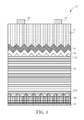
- FIG. 1 illustrates a schematic diagram of a solar cell according to an exemplary embodiment of the present invention.
- the solar cell 10 of the exemplary embodiment includes a crystalline semiconductor substrate 12; a first crystalline semiconductor layer 14; an amorphous semiconductor layer 16; a first metal electrode layer 18 and a second metal electrode layer 20.
- the crystalline semiconductor substrate 12 has a first surface 121 and a second surface 122, and the crystalline semiconductor substrate 12 has a first doped type.
- the lattice vector of the crystalline semiconductor substrate 12 can be such as (1,0,0), (1,1,0), (1,1,1), etc., but not limited thereto.
- the crystalline semiconductor substrate 12 may be a wafer, a die or any other types of semiconductor substrates.
- the first crystalline semiconductor layer 14 is disposed on the first surface 121 of the crystalline semiconductor substrate 12, where the first crystalline semiconductor layer 14 has a second doped type contrary to the first doped type.
- the first doped type can be P type
- the second doped type is N type, but not limited thereto, or the first doped type can also be N type, while the second doped type is P type. Because of the difference in the doped types between the crystalline semiconductor substrate 12 and the first crystalline semiconductor layer 14, a PN junction occurs in the interface between the crystalline semiconductor substrate 12 and the first crystalline semiconductor layer 14.
- the crystalline semiconductor substrate 12 and the first crystalline semiconductor layer 14 are both made of crystalline semiconductor materials.
- at least one of the crystalline semiconductor substrate 12 and the first crystalline semiconductor layer 14 is made of single crystalline silicon or poly crystalline silicon.
- the materials of the crystalline semiconductor substrate 12 and the first crystalline semiconductor layer 14 are preferably the same, for example, the crystalline semiconductor substrate 12 and the first crystalline semiconductor layer 14 are both made of single crystalline silicon, or the crystalline semiconductor substrate 12 and the first crystalline semiconductor layer 14 are both made of poly crystalline silicon.
- the material of the crystalline semiconductor substrate 12 and the material of the first crystalline semiconductor layer 14 can be different, which may lead to inferior power conversion efficiency.
- the dopant concentration of the crystalline semiconductor substrate 12 may be substantially the same as the dopant concentration of the first crystalline semiconductor layer 14, but not limited thereto.
- the dopant concentration of the crystalline semiconductor substrate 12 and the dopant concentration of the first crystalline semiconductor layer 14 can be substantially different, which may lead to inferior power conversion efficiency.
- the dopant concentration of the crystalline semiconductor substrate 12 is approximately between 10 14 atoms/cm 2 and 10 17 atoms/cm 2
- the dopant concentration of the first crystalline semiconductor layer 14 is approximately between 10 17 atoms/cm 2 and 10 21 atoms/cm 2 , but not limited thereto.
- the thickness of the crystalline semiconductor substrate 12 is approximately between 50 micrometer ( ⁇ m) and 500 ⁇ m, but not limited thereto.
- the thickness of the first crystalline semiconductor layer 14 is approximately larger than 0 nanometer (nm) and less than or equal to 500 nm, for instance, preferably larger than 0 nm and less than or equal to 200 nm, and more preferably about 15 nm, but not limited thereto.
- the amorphous semiconductor layer 16 is disposed on the first crystalline semiconductor layer 14, and the amorphous semiconductor layer 16 has the second doped type. In this exemplary embodiment, the thickness of the amorphous semiconductor layer 16 is approximately between 1 nm and 20 nm, but not limited thereto.
- the dopant concentration of the amorphous semiconductor layer 16 is higher than the dopant concentration of the first crystalline semiconductor layer 14.
- the dopant concentration of the amorphous semiconductor layer 16 is substantially between 10 18 atoms/cm 2 and 10 21 atoms/cm 2 .
- the first metal electrode layer 18 is disposed on the amorphous semiconductor layer 16, and the second metal electrode layer 20 is disposed on the second surface 122 of the crystalline semiconductor substrate 12.
- the first metal electrode layer 18 and the second metal electrode layer 20 may be made of metal with excellent conductivity, such as aluminum (A1), silver (Ag), platinum (Pt), aurum (Au), alloy of above metal elements, or any other suitable materials, but not limited thereto.
- the thickness, the area and the pattern of the first metal electrode layer 18 and the second metal electrode layer 20 are all adjustable on the basis of requirements.
- the solar cell 10 may further include a passivation layer 22 disposed between the amorphous semiconductor layer 16 and the first metal electrode layer 18.
- the passivation layer 22 may be a single-layered structure or a multi-layered structure.
- the passivation layer 22 may include, but not limited thereto, transparent conducting material such as Indium Tin Oxide (ITO), Indium Zinc Oxide (IZO), Antimony Tin Oxide (ATO), Aluminum Zinc Oxide (AZO), Indium Gallium Zinc Oxide (IGZO), etc.
- the thickness of transparent conducting material is, for example, approximately between 10 nm and 500 nm.
- the material of the passivation layer 22 may also include, but not limited thereto, anti-reflective material such as silicon oxide, silicon nitride, or silicon oxynitride.
- the passivation layer 22 is necessary to utilize substantially transparent material, because if the passivation layer 22 utilizes opaque material, the solar cell 10 cannot perform energy conversion process.
- the solar cell 10 of this exemplary embodiment may also include a second semiconductor layer 24 disposed between the crystalline semiconductor substrate 12 and the second metal electrode layer 20. The second semiconductor layer 24 is electrically connected to the crystalline semiconductor substrate 12 and the second metal electrode layer 20 for reducing the contact resistance. If there is no concern about contact resistance, the disposition of the second semiconductor layer 24 is no longer necessary.
- the material of the second semiconductor layer 24 can include amorphous silicon, and the thickness of second semiconductor layer 24 is approximately between 1 ⁇ m and 50 ⁇ m, but not limited thereto. Further, the second semiconductor layer 24 has the first doped type, and the dopant concentration of the second semiconductor layer 24 is preferably higher than the dopant concentration of the crystalline semiconductor substrate 12. In this exemplary embodiment, for instance, the dopant concentration of the second semiconductor layer 24 is substantially between 10 17 atoms/cm 2 and 10 21 atoms/cm 2 .
- the interface between two adjacent film layers in the solar cell 10 such as the interface between the crystalline semiconductor substrate 12 and the first crystalline semiconductor layer 14, the interface between the first crystalline semiconductor layer 14 and the amorphous semiconductor layer 16, the interface between the crystalline semiconductor substrate 12 and the second semiconductor layer 24 and so on, can alternatively undergo a textured process for increasing the amount of incident light, but not limited thereto. If the power conversion efficiency of the solar cell 10 is high enough, the utilization of the textured process is optional, surely, the additional implementation of textured process induces better power conversion efficiency.
- the PN junction of the solar cell 10 occurs between the crystalline semiconductor substrate 12 and the first crystalline semiconductor layer 14, that is, the depletion region is located in the interface between the crystalline semiconductor substrate 12 and the first crystalline semiconductor layer 14.
- the homo-junction between the crystalline semiconductor substrate 12 and the first crystalline semiconductor layer 14 is unfavorable for generation of interface traps, while the hetero-junction between the first crystalline semiconductor layer 14 and the amorphous semiconductor layer 16 is favorable for generation of interface traps.
- the depletion region is far away from the hetero-junction between the first crystalline semiconductor layer 14 and the amorphous semiconductor layer 16, the recombination of electron-hole pairs can be induced. Therefore, the less recombination of electron-hole pairs induces a higher open-circuit voltage of solar cell, and improves the power conversion efficiency.
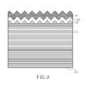
- FIG. 2-FIG. 4 illustrate schematic diagrams of a method of forming a solar cell according to an exemplary embodiment of the present invention.
- a crystalline semiconductor substrate 12 with a first doped type is provided.
- the textured process may be implemented on a first surface 121 of the crystalline semiconductor substrate 12.
- the textured process also may be omitted as mentioned before.
- an amorphous semiconductor layer 16 with a second doped type is formed on the first surface 121 of the crystalline semiconductor layer 12.
- an annealing process is then performed to diffuse the dopant of the amorphous semiconductor layer 16 along the direction toward the crystalline semiconductor substrate 12 for forming a first crystalline semiconductor layer 14 in the first surface 121 of the crystalline semiconductor substrate 12.
- the first crystalline semiconductor layer 14 and the crystalline semiconductor substrate 12 possess the same crystalline type, but contrary doped type. Therefore, a PN junction occurs between the crystalline semiconductor substrate 12 and the first crystalline semiconductor layer 14, i.e. the depletion region is located in the interface between the crystalline semiconductor substrate 12 and the first crystalline semiconductor layer 14.
- a passivation layer 22 may be selectively formed on the amorphous semiconductor layer 16, and further, a first metal electrode layer 18 is formed on the passivation layer 22. Additionally, the textured process may be selectively implemented on a second surface 122 of the crystalline semiconductor substrate 12. Subsequently, a second semiconductor layer 24 is formed on the second surface 122 of the crystalline semiconductor substrate 12, and a second metal electrode layer 20 is formed on the second semiconductor layer 24. Accordingly, the solar cell 40 of this exemplary embodiment is fabricated.
- FIG. 5-FIG. 6 illustrate schematic diagrams of a method of forming a solar cell according to another exemplary embodiment of the present invention.
- a crystalline semiconductor substrate 12 with a first doped type is provided.
- a first crystalline semiconductor layer 14 with a second doped type contrary to the first doped type is formed on a first surface 121 of the crystalline semiconductor substrate 12.
- the material of the crystalline semiconductor substrate 12 and the material of the first crystalline semiconductor layer 14 could be the same. Using different materials for the crystalline semiconductor substrate 12 and the material of the first crystalline semiconductor layer 14 is also acceptable; however, the difference might be unfavorable to the energy conversion efficiency.
- an amorphous semiconductor layer 16 with the second doped type is formed on the first crystalline semiconductor layer 14.
- a passivation layer 22 is selectively formed on the amorphous semiconductor layer 16, and a first metal electrode layer 18 is formed on the passivation layer 22.
- a second semiconductor layer 24 may be optionally formed on a second surface 122 of the crystalline semiconductor substrate 12, and a second metal electrode layer 20 is formed on the second semiconductor layer 24. Accordingly, the solar cell 50 of this exemplary embodiment is fabricated.
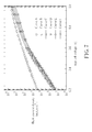
- FIG. 7 is a simulation diagram illustrating a relation between a dark current density and an applied voltage of a solar cell according to an exemplary embodiment of the present invention.
- the interface trap density (Dit) is substantially kept as 5*10 13 (#/cm 2 eV)
- curve A represents the relation between the dark current density and the applied voltage of the solar cell under the condition where the thickness of the first crystalline semiconductor layer is 0 (i.e. the first crystalline semiconductor layer does not exist)
- curves B-F represent the relation between the dark current density and the applied voltage of the solar cell under the condition where the thickness of the first crystalline semiconductor layer is 15 nm, 25 nm, 50 nm, 100 nm and 200 nm, respectively.
- the dark current density (curve B-curve F) of the solar cell having the first crystalline semiconductor layer is obviously lower than the dark current density (curve A) of the solar cell without the first crystalline semiconductor layer. Therefore, the effect of the first crystalline semiconductor layer upon the decrease of dark current density is proven.
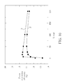
- FIG. 8 is a simulation diagram illustrating a relation between an open-circuit voltage V oc and a thickness X of a first crystalline semiconductor layer of a solar cell according to an exemplary embodiment of the present invention.
- Curve 1 is obtained under the condition where the interface trap density (Dit) is about 2*10 13 (#/cm2eV), and curve 1' is obtained under the condition where the interface trap density is about 2.5 * 10 13 (#/cm 2 eV).
- the interface trap density Dit
- curve 1' is obtained under the condition where the interface trap density is about 2.5 * 10 13 (#/cm 2 eV).
- the corresponding open-circuit voltage V oc of the solar cell is substantially between 620 mV and 700mV.
- FIG. 9 is a simulation diagram illustrating a relation between a current density J sc and a thickness X of a first crystalline semiconductor layer of a solar cell according to an exemplary embodiment of the present invention.
- Curve 2 is obtained under the condition where the interface trap density (Dit) is about 2*10 13 (#/cm2eV), and curve 2' is obtained under the condition where the interface trap density is about 2.5*10 13 (#/cm 2 eV). As shown in FIG.
- the corresponding current density J sc of the solar cell is substantially between 29 mA/cm 2 and 32 mA/cm 2 .
- FIG. 10 is a simulation diagram illustrating a relation between a power conversion efficiency and a thickness X of a first crystalline semiconductor layer of a solar cell according to an exemplary embodiment of the present invention.
- Curve 3 is obtained under the condition where the interface trap density (Dit) is about 2*10 13 (#/cm 2 eV), and curve 3' is obtained under the condition where the interface trap density is about 2.5*10 13 (#/cm 2 eV).
- the thickness X of the first crystalline semiconductor layer is approximately larger than 0 nm and less than or equal to 200 nm, the corresponding power conversion efficiency of the solar cell is substantially between 15% and 17.5%.
- the thickness X of the first crystalline semiconductor layer is between 10 nm and 20 nm, such as about 15nm, the power conversion efficiency of the solar cell reaches to 17.5% substantially.
- the depletion region of the solar cell of the present invention is located in the homo-junction interface between the crystalline semiconductor substrate and the first crystalline semiconductor layer, which is away from the hetero-junction between the first crystalline semiconductor layer and the amorphous semiconductor layer.
Landscapes
- Photovoltaic Devices (AREA)
Applications Claiming Priority (1)
| Application Number | Priority Date | Filing Date | Title |
|---|---|---|---|
| TW099136520A TWI455329B (zh) | 2010-10-26 | 2010-10-26 | 太陽能電池及其製作方法 |
Publications (1)
| Publication Number | Publication Date |
|---|---|
| EP2448005A2 true EP2448005A2 (de) | 2012-05-02 |
Family
ID=45440634
Family Applications (1)
| Application Number | Title | Priority Date | Filing Date |
|---|---|---|---|
| EP11163653A Withdrawn EP2448005A2 (de) | 2010-10-26 | 2011-04-26 | Solarzelle und Verfahren zu deren Herstellung |
Country Status (3)
| Country | Link |
|---|---|
| US (1) | US20120097246A1 (de) |
| EP (1) | EP2448005A2 (de) |
| TW (1) | TWI455329B (de) |
Families Citing this family (1)
| Publication number | Priority date | Publication date | Assignee | Title |
|---|---|---|---|---|
| US11444212B2 (en) * | 2018-06-22 | 2022-09-13 | Jingao Solar Co., Ltd. | Crystalline silicon solar cell and preparation method therefor, and photovoltaic module |
Family Cites Families (8)
| Publication number | Priority date | Publication date | Assignee | Title |
|---|---|---|---|---|
| US4539431A (en) * | 1983-06-06 | 1985-09-03 | Sera Solar Corporation | Pulse anneal method for solar cell |
| JP3902534B2 (ja) * | 2001-11-29 | 2007-04-11 | 三洋電機株式会社 | 光起電力装置及びその製造方法 |
| EP1398837A1 (de) * | 2002-09-09 | 2004-03-17 | Interuniversitair Microelektronica Centrum ( Imec) | Photovoltaische Vorrichtung |
| KR101000064B1 (ko) * | 2007-12-18 | 2010-12-10 | 엘지전자 주식회사 | 이종접합 태양전지 및 그 제조방법 |
| US7964499B2 (en) * | 2008-05-13 | 2011-06-21 | Samsung Electronics Co., Ltd. | Methods of forming semiconductor solar cells having front surface electrodes |
| WO2009152238A2 (en) * | 2008-06-11 | 2009-12-17 | E. I. Du Pont De Nemours And Company | A process of forming a silicon solar cell |
| KR20100013649A (ko) * | 2008-07-31 | 2010-02-10 | 삼성전자주식회사 | 광전소자 및 이의 제조 방법 |
| US20100132774A1 (en) * | 2008-12-11 | 2010-06-03 | Applied Materials, Inc. | Thin Film Silicon Solar Cell Device With Amorphous Window Layer |
-
2010
- 2010-10-26 TW TW099136520A patent/TWI455329B/zh not_active IP Right Cessation
-
2011
- 2011-03-29 US US13/074,015 patent/US20120097246A1/en not_active Abandoned
- 2011-04-26 EP EP11163653A patent/EP2448005A2/de not_active Withdrawn
Non-Patent Citations (1)
| Title |
|---|
| None |
Also Published As
| Publication number | Publication date |
|---|---|
| TW201218390A (en) | 2012-05-01 |
| US20120097246A1 (en) | 2012-04-26 |
| TWI455329B (zh) | 2014-10-01 |
Similar Documents
| Publication | Publication Date | Title |
|---|---|---|
| US10084107B2 (en) | Transparent conducting oxide for photovoltaic devices | |
| KR101139443B1 (ko) | 이종접합 태양전지와 그 제조방법 | |
| CN103137767B (zh) | 全背电极异质结太阳能电池 | |
| US20100243042A1 (en) | High-efficiency photovoltaic cells | |
| US8835753B2 (en) | Solar cell and method of fabricating the same | |
| KR100850641B1 (ko) | 고효율 결정질 실리콘 태양전지 및 그 제조방법 | |
| CN205920977U (zh) | 一种具有新型发射极的硅异质结太阳能电池及光伏组件 | |
| CN107369726B (zh) | n型晶体硅双面太阳电池 | |
| KR101886818B1 (ko) | 이종 접합 실리콘 태양 전지의 제조 방법 | |
| KR20130016848A (ko) | Hit 태양전지 | |
| Muñoz et al. | Key aspects on development of high efficiency heterojunction and IBC heterojunction solar cells: Towards 22% efficiency on industrial size | |
| CN104272469B (zh) | 太阳能电池装置及其制造方法 | |
| RU2590284C1 (ru) | Солнечный элемент | |
| CN102403370A (zh) | 共面式光伏电池及其制造方法 | |
| CN102201480A (zh) | 基于n型硅片的碲化镉半导体薄膜异质结太阳电池 | |
| EP2448005A2 (de) | Solarzelle und Verfahren zu deren Herstellung | |
| Veschetti et al. | Industrial process leading to 19.8% on n-type CZ silicon | |
| Lu et al. | a-Si/c-Si heterojunction for interdigitated back contact solar cell | |
| Stangl et al. | Thin film silicon emitters for crystalline silicon solar cells, epitaxial, amorphous or microcrystalline?-a simulation study | |
| EP2506313A1 (de) | Solarzelle und verfahren zu ihrer herstellung | |
| Hertanto et al. | Back amorphous-crystalline silicon heterojunction (BACH) photovoltaic device | |
| CN102064211B (zh) | 太阳能电池及其制作方法 | |
| US20140053895A1 (en) | Intentionally-doped cadmium oxide layer for solar cells | |
| EP2608273A2 (de) | Solarzelle mit einem PN-Heteroübergang | |
| CN104054182B (zh) | 太阳能电池设备及其制造方法 |
Legal Events
| Date | Code | Title | Description |
|---|---|---|---|
| PUAI | Public reference made under article 153(3) epc to a published international application that has entered the european phase |
Free format text: ORIGINAL CODE: 0009012 |
|
| 17P | Request for examination filed |
Effective date: 20110426 |
|
| AK | Designated contracting states |
Kind code of ref document: A2 Designated state(s): AL AT BE BG CH CY CZ DE DK EE ES FI FR GB GR HR HU IE IS IT LI LT LU LV MC MK MT NL NO PL PT RO RS SE SI SK SM TR |
|
| AX | Request for extension of the european patent |
Extension state: BA ME |
|
| RIN1 | Information on inventor provided before grant (corrected) |
Inventor name: LIANG, SHUO-WEI Inventor name: HO, WEI-SHUO Inventor name: KU, CHUN-YUAN Inventor name: LIU, CHEE-WEE Inventor name: CHEN, TSUNG-PAO Inventor name: CHEN, YEN-YU Inventor name: CHEN, JEN-CHIEH Inventor name: WU, ZHEN-CHENG Inventor name: LAI, CHUNG-WEI |
|
| STAA | Information on the status of an ep patent application or granted ep patent |
Free format text: STATUS: REQUEST FOR EXAMINATION WAS MADE |
|
| STAA | Information on the status of an ep patent application or granted ep patent |
Free format text: STATUS: THE APPLICATION IS DEEMED TO BE WITHDRAWN |
|
| 18D | Application deemed to be withdrawn |
Effective date: 20171103 |