EP2448098A2 - Stromversorgung mit einstufigem Wandler zur Durchführung der Leistungsfaktorkorrektur und Resonanzwandler - Google Patents
Stromversorgung mit einstufigem Wandler zur Durchführung der Leistungsfaktorkorrektur und Resonanzwandler Download PDFInfo
- Publication number
- EP2448098A2 EP2448098A2 EP11001096A EP11001096A EP2448098A2 EP 2448098 A2 EP2448098 A2 EP 2448098A2 EP 11001096 A EP11001096 A EP 11001096A EP 11001096 A EP11001096 A EP 11001096A EP 2448098 A2 EP2448098 A2 EP 2448098A2
- Authority
- EP
- European Patent Office
- Prior art keywords
- power supply
- power
- circuit
- voltage
- output
- Prior art date
- Legal status (The legal status is an assumption and is not a legal conclusion. Google has not performed a legal analysis and makes no representation as to the accuracy of the status listed.)
- Withdrawn
Links
- 238000006243 chemical reaction Methods 0.000 title abstract description 16
- 239000003990 capacitor Substances 0.000 claims description 29
- 230000001105 regulatory effect Effects 0.000 claims description 10
- 238000002955 isolation Methods 0.000 claims description 4
- 230000001276 controlling effect Effects 0.000 claims description 3
- 239000003381 stabilizer Substances 0.000 claims description 3
- 230000001629 suppression Effects 0.000 claims description 3
- 230000000087 stabilizing effect Effects 0.000 claims description 2
- 238000010586 diagram Methods 0.000 description 7
- 238000001914 filtration Methods 0.000 description 7
- 238000004804 winding Methods 0.000 description 7
- 230000004048 modification Effects 0.000 description 3
- 238000012986 modification Methods 0.000 description 3
- 230000003247 decreasing effect Effects 0.000 description 2
- 238000004519 manufacturing process Methods 0.000 description 2
- 230000033228 biological regulation Effects 0.000 description 1
- 230000000903 blocking effect Effects 0.000 description 1
- 230000001939 inductive effect Effects 0.000 description 1
- 238000005070 sampling Methods 0.000 description 1
Images


Classifications
-
- H—ELECTRICITY
- H02—GENERATION; CONVERSION OR DISTRIBUTION OF ELECTRIC POWER
- H02M—APPARATUS FOR CONVERSION BETWEEN AC AND AC, BETWEEN AC AND DC, OR BETWEEN DC AND DC, AND FOR USE WITH MAINS OR SIMILAR POWER SUPPLY SYSTEMS; CONVERSION OF DC OR AC INPUT POWER INTO SURGE OUTPUT POWER; CONTROL OR REGULATION THEREOF
- H02M1/00—Details of apparatus for conversion
- H02M1/42—Circuits or arrangements for compensating for or adjusting power factor in converters or inverters
- H02M1/4208—Arrangements for improving power factor of AC input
- H02M1/4258—Arrangements for improving power factor of AC input using a single converter stage both for correction of AC input power factor and generation of a regulated and galvanically isolated DC output voltage
-
- H—ELECTRICITY
- H02—GENERATION; CONVERSION OR DISTRIBUTION OF ELECTRIC POWER
- H02M—APPARATUS FOR CONVERSION BETWEEN AC AND AC, BETWEEN AC AND DC, OR BETWEEN DC AND DC, AND FOR USE WITH MAINS OR SIMILAR POWER SUPPLY SYSTEMS; CONVERSION OF DC OR AC INPUT POWER INTO SURGE OUTPUT POWER; CONTROL OR REGULATION THEREOF
- H02M3/00—Conversion of DC power input into DC power output
- H02M3/22—Conversion of DC power input into DC power output with intermediate conversion into AC
- H02M3/24—Conversion of DC power input into DC power output with intermediate conversion into AC by static converters
- H02M3/28—Conversion of DC power input into DC power output with intermediate conversion into AC by static converters using discharge tubes with control electrode or semiconductor devices with control electrode to produce the intermediate AC
- H02M3/325—Conversion of DC power input into DC power output with intermediate conversion into AC by static converters using discharge tubes with control electrode or semiconductor devices with control electrode to produce the intermediate AC using devices of a triode or a transistor type requiring continuous application of a control signal
- H02M3/335—Conversion of DC power input into DC power output with intermediate conversion into AC by static converters using discharge tubes with control electrode or semiconductor devices with control electrode to produce the intermediate AC using devices of a triode or a transistor type requiring continuous application of a control signal using semiconductor devices only
- H02M3/337—Conversion of DC power input into DC power output with intermediate conversion into AC by static converters using discharge tubes with control electrode or semiconductor devices with control electrode to produce the intermediate AC using devices of a triode or a transistor type requiring continuous application of a control signal using semiconductor devices only in push-pull configuration
- H02M3/3376—Conversion of DC power input into DC power output with intermediate conversion into AC by static converters using discharge tubes with control electrode or semiconductor devices with control electrode to produce the intermediate AC using devices of a triode or a transistor type requiring continuous application of a control signal using semiconductor devices only in push-pull configuration with automatic control of output voltage or current
-
- H—ELECTRICITY
- H02—GENERATION; CONVERSION OR DISTRIBUTION OF ELECTRIC POWER
- H02M—APPARATUS FOR CONVERSION BETWEEN AC AND AC, BETWEEN AC AND DC, OR BETWEEN DC AND DC, AND FOR USE WITH MAINS OR SIMILAR POWER SUPPLY SYSTEMS; CONVERSION OF DC OR AC INPUT POWER INTO SURGE OUTPUT POWER; CONTROL OR REGULATION THEREOF
- H02M1/00—Details of apparatus for conversion
- H02M1/0048—Circuits or arrangements for reducing losses
- H02M1/0054—Transistor switching losses
-
- Y—GENERAL TAGGING OF NEW TECHNOLOGICAL DEVELOPMENTS; GENERAL TAGGING OF CROSS-SECTIONAL TECHNOLOGIES SPANNING OVER SEVERAL SECTIONS OF THE IPC; TECHNICAL SUBJECTS COVERED BY FORMER USPC CROSS-REFERENCE ART COLLECTIONS [XRACs] AND DIGESTS
- Y02—TECHNOLOGIES OR APPLICATIONS FOR MITIGATION OR ADAPTATION AGAINST CLIMATE CHANGE
- Y02B—CLIMATE CHANGE MITIGATION TECHNOLOGIES RELATED TO BUILDINGS, e.g. HOUSING, HOUSE APPLIANCES OR RELATED END-USER APPLICATIONS
- Y02B70/00—Technologies for an efficient end-user side electric power management and consumption
- Y02B70/10—Technologies improving the efficiency by using switched-mode power supplies [SMPS], i.e. efficient power electronics conversion e.g. power factor correction or reduction of losses in power supplies or efficient standby modes
-
- Y—GENERAL TAGGING OF NEW TECHNOLOGICAL DEVELOPMENTS; GENERAL TAGGING OF CROSS-SECTIONAL TECHNOLOGIES SPANNING OVER SEVERAL SECTIONS OF THE IPC; TECHNICAL SUBJECTS COVERED BY FORMER USPC CROSS-REFERENCE ART COLLECTIONS [XRACs] AND DIGESTS
- Y02—TECHNOLOGIES OR APPLICATIONS FOR MITIGATION OR ADAPTATION AGAINST CLIMATE CHANGE
- Y02P—CLIMATE CHANGE MITIGATION TECHNOLOGIES IN THE PRODUCTION OR PROCESSING OF GOODS
- Y02P80/00—Climate change mitigation technologies for sector-wide applications
- Y02P80/10—Efficient use of energy, e.g. using compressed air or pressurized fluid as energy carrier
Definitions
- the invention relates to a power supply, and more particularly to a power supply with a single stage converter for performing power factor correction and resonant conversion.
- the conventional high-voltage power supply generally employs a two-stage converter to convert an input voltage into an output voltage.
- a power supply 100 is configured to convert an AC voltage Vin into an output voltage Vo.
- the power supply 100 includes a bridge rectifier 120, a power factor correction converter 140, a resonant converter 160, a transformer T100, and an output capacitor C100.
- the output voltage Vo is used to drive a load Z100.
- the bridge rectifier 120 is configured to rectify the AC voltage Vin into a full-wave rectified DC voltage.
- the power factor correction converter 140 is connected to the output end of the bridge rectifier 120 and includes a boost choke Ls, a control switch S100, a diode D100, and a filtering capacitor Cs.
- the boost choke Ls is used to store the full-wave rectified DC voltage outputted from the bridge rectifier 120 and transfer the stored energy to the filtering capacitor Cs through the diode D100 according to the switching operation of the control switch S100. With the capacitive impedance of the filtering capacitor Cs, the high-frequency harmonics of the input current can be suppressed, thereby improving the power factor of the input voltage Vin.
- the resonant converter 160 is connected to the output end of the power factor correction converter 140 and includes control switches S102, S104, filtering capacitors C1, C2, a resonant inductor Lr, and resonant capacitors Cs, Cp.
- the resonant tank formed by the resonant inductor Lr and the resonant capacitors Cs, Cp is used to generate resonance to drive the control switches S102, S104 to switch at the time when the voltage or current of the resonant tank is zero, thereby reducing the switching loss and accomplishing the voltage conversion.
- the energy of the AC voltage Vin can be transferred to the secondary side of the transformer.
- the transformer T100 includes a primary winding Np100 and a secondary winding Ns100, in which the primary winding Np100 is used to store the energy of the AC voltage Vin transmitted from the resonant converter 160 and transfer the stored energy to the secondary winding Ns100 according to the switching operation of the control switches S102, S104, thereby inducing a voltage across the secondary winding Ns100. Therefore, the induced voltage is outputted to the load Z100 through the output capacitor C100, and thus the load Z100 is powered.
- the power supply of Fig. 1 is made up of a two-stage converter in which the first stage converter is implemented by a power factor correction converter 140 and the second stage converter is implemented by a resonant converter 160.
- the power conversion efficiency of the power supply of Fig. 1 is derived as the product of the power conversion efficiency of the first stage converter and the power conversion efficiency of the second stage converter. Therefore, the power conversion efficiency of the power supply of Fig. 1 is lessened as a result of the multiplication.
- the two-stage converter is employed to achieve the power conversion for the power supply, the number of the circuit elements of the power supply is increased, thereby inflating the cost and boosting power loss.
- An aspect of the invention is to provide a power supply with a single stage converter for performing power factor correction and resonant conversion to lower power loss, descend cost, or reduce the number of circuit elements.
- one embodiment of the invention provides a power supply having a single stage converter connected to an input voltage, in which the single stage converter includes a switch circuit capable of transferring the energy of the input voltage according to the switching operation of the switch circuit.
- the power supply also includes a transformer connected to the single stage converter and having a primary side and a secondary side for storing the energy transferred from the single stage converter at the primary side and transferring the energy stored at the primary side to the secondary side according to the switching operation of the switch circuit, thereby generating an output voltage.
- the single stage converter also includes a resonant circuit connected between the switch circuit and the primary side of the transformer for generating resonance to transfer the energy of the input voltage to the primary side of the transformer.
- the single stage converter also includes a power control circuit for comparing an input current sensing signal indicative of a sensed input current of the power supply and a power level control input to generate a frequency modulation control signal.
- the frequency modulation control signal is capable of controlling of the output power of the power supply and the suppression of harmonics of the input current of the power supply.
- the single stage converter also includes a square wave generator connected to the power control circuit for generating a driving signal for driving the switch circuit according to the frequency modulation control signal, in which the frequency of the driving signal is varied synchronously with the frequency of the frequency modulation control signal.
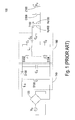
- Fig. 1 is a circuit block diagram showing a power supply with a two-stage converter according to the prior art
- Fig. 2 is a circuit block diagram showing a power supply with a single-stage converter according to a first embodiment of the invention
- Fig. 3 is a circuit diagram showing the circuitry of the power control circuit according the first embodiment of the invention.
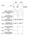
- Fig. 4 shows the current waveforms and voltage waveforms measured at the circuit nodes of the power supply according to the first embodiment of the invention
- Fig. 5 is a circuit block diagram showing a power supply with a single-stage converter according to a second embodiment of the invention.
- Fig. 6 is a circuit block diagram showing a power supply with a single-stage converter according to a third embodiment of the invention.
- Fig. 7 is a circuit block diagram showing a power supply with a single-stage converter according to a fourth embodiment of the invention.
- Fig. 8 is a circuit block diagram showing a power supply with a single-stage converter according to a fifth embodiment of the invention.
- Fig. 2 shows the circuit blocks of the power supply 200 according to a first embodiment of the invention. It should be noted that the same reference number is given to label similar circuit elements throughout the entire specification.
- an input AC voltage Vin is supplied to the input terminal of the power supply.
- the power supply 200 is configured to convert the AC voltage Vin into an output voltage Vo developed across the output capacitor C200 for powering the load Z200.
- the power supply 200 includes a bridge rectifier 204 for rectifying the input AC voltage Vin into a full-wave rectified DC voltage.
- the power supply 200 further includes a filtering inductor 206 and a filtering capacitor 212 that constitute a filter circuit and are connected to the output end of the bridge rectifier 204 for suppressing the electromagnetic interference and the high-frequency noises of the input AC voltage Vin and generating a DC Voltage V DC analogous to the full-wave rectified DC voltage outputted from the bridge rectifier 204 or the half-wave rectified DC voltage generated by half-wave rectifying the input voltage Vin.
- the filter circuit (206, 212) may be used to remove high-frequency noises with frequency above the frequency of the input voltage Vin (for example 60Hz).
- the power supply 200 also includes a current sensor 230 for sensing the input current Iin and thus generating an input current sensing signal Va indicative of the sensed input current.
- the power supply 200 also includes a switch circuit 208 consisted of a high-side switch 2081 and a low-side switch 2082.
- the power supply 200 also includes a transformer T200 having a primary winding Np200 and a secondary winding Ns200.
- the power supply 200 also includes a LLC resonant tank 213 which may be a series LLC resonant circuit or a parallel LLC resonant circuit.
- the LLC resonant tank consists of a first resonant capacitor Cs1, a first resonant inductor Ls1, and a second resonant inductor Lm.
- one end of the first resonant capacitor Cs1 is connected to a junction node located between the high-side switch 2081 and the low-side switch 2082, and the other end of the first resonant capacitor Cs1 is connected to one end of the first resonant inductor Ls1.
- One end of the first resonant inductor Ls1 is connected to the other end of the first resonant capacitor Cs1, and the other end of first resonant inductor Ls1 is connected to the primary side Np200 of the transformer T200.
- the first resonant inductor Ls1 may be the leakage inductance of the transformer T200 and the second resonant inductor Lm may be the magnetizing inductance of the transformer T200.
- the first resonant capacitor Cs1 may function as a DC blocking capacitor for preventing the DC component of the input AC voltage Vin to enter the transformer T200.
- the LLC resonant tank 213 is used to transfer the energy of the input AC voltage Vin to the primary side Np200 of the transformer T200 by way of resonance according to the switching operation of the switch circuit 208.
- the high-side switch 2081 and the low-side switch 2082 of the switch circuit 208 are configured to switch alternately. That is, the high-side switch 2081 and the low-side switch 2082 of the switch circuit 208 are turned on and off in an alternate way.
- the power supply 200 also includes a power control circuit 250 and a square wave generator 260 that constitute a control circuit.
- the power control circuit 250 is used to receive the input current sensing signal Va from the current sensor 230 and an external power level control input for generating a frequency modulation control signal 306.
- the square wave generator 260 is connected between the power control circuit 250 and the control terminal of the switch circuit 208 for generating a driving signal for driving the switch circuit 208 according to the frequency modulation control signal 306. The frequency of the driving signal is varied synchronously with the frequency of the frequency modulation control signal 306.
- the frequency modulation control signal 306 is varied depending on the input current sensing signal Va and the external power level control input, the frequency of the driving signal is varied depending on the input current sensing signal Va and the external power level control input.
- the frequency modulation control signal 306 carries the information about the power control and the waveform analogous to the full-wave rectified DC voltage outputted from the bridge rectifier 204, the frequency modulation control signal 306 can be used for the control of output power of the power supply 200 and the suppression of the harmonics of the input current Iin.
- the power control circuit 250 and the square wave generator 260 fulfill the demands of power factor correction for the input voltage Vin.
- the inventive power supply has less circuit elements, lower manufacturing cost, or better power conversion efficiency.
- Fig. 3 shows the circuitry of the power control circuit 250.
- the power control circuit 250 includes a proportional differential circuit (proportional subtractor circuit) and a reverse current isolation device 304.
- the proportional subtractor circuit includes a power amplifier (or an operational amplifier) 302, a plurality of resistors R31-R35, and a plurality of capacitors C31-C37. It should be noted that the proportional differential circuit is configured in a negative feedback topology.
- the power amplifier 302 has a negative input terminal for receiving the input current sensing signal Va from the input current sensor 230 and a positive input terminal for receiving the external power level control input.
- the external power level control input represents the magnitude of the output power desired by the user.
- the power amplifier 302 is configured to compare the input current sensing signal Va outputted from the input current sensor 230 and the external power level control input inputted by the user, and output the frequency modulation control signal 306 in response to the comparison.
- the frequency modulation control signal 306 is the proportional difference between the power level control input and the input current sensing signal Va.
- the reverse current isolation device 304 is an optional element and may be implemented by a diode. The reverse current isolation device 304 is connected between the power amplifier 302 and the square wave generator 260 for preventing a reverse current from flowing from the square wave generator 260 to the power amplifier 302.
- the frequency modulation control signal 306 is transmitted to the square wave generator 260 in order to allow the square wave generator 260 to regulate the switching frequency of the driving signal used to drive the switch circuit 208 according to the frequency modulation control signal 306, and suppress the harmonics of the input current Iin accordingly.
- Figs. 4A-4H illustrate the current waveforms and voltage waveforms measured at the circuit nodes of the power supply disclosed in the foregoing embodiment.
- Fig. 4A illustrates the voltage waveform of the DC voltage V DC which is generated by removing the high-frequency noises from the full-wave rectified DC voltage outputted from the bridge rectifier 204.
- the frequency of the DC voltage V DC is, for example, 60Hz or 120Hz, and is equal to or double of the frequency of the input AC voltage Vin.
- Fig. 4B shows the current waveform of the uncorrected input current Iin as the power control circuit 250 and the square wave generator 260 is not applied to the power supply, and Fig.
- FIG. 4C shows the current waveform of the corrected input current Iin as the power control circuit 250 and the square wave generator 260 is applied to the power supply. It can be readily known from Figs. 4B and 4C that as the power control circuit 250 and the square wave generator 260 is applied to the AC-DC converter, the current waveform of the input current of Fig. 4B will be smoothed and resembles the voltage waveform of the DC voltage V DC of Fig. 4A or the full-wave DC voltage generated by full-wave rectifying the input voltage Vin. As shown in Fig. 4C , the waveform of the corrected input current is analogous to the waveform of a sinusoidal wave after being full-wave rectified, and the high-frequency noises of the input current is suppressed. Fig.
- FIG. 4F shows the current waveform of the input current sensing signal Va which is derived by sampling or attenuating the corrected input current Iin of Fig. 4C.
- Fig. 4G shows the waveform of the power level control input inputted by the user which indicates the magnitude of the output power desired by the user.
- Fig. 4H shows the waveform of the frequency modulation control signal 306 outputted from the power amplifier 302.
- Fig. 4D is the waveform of the driving signal of the high-side switch 2081
- Fig. 4E is the waveform of the driving signal of the low-side switch 2082. It can be understood from Figs. 4D and 4E that the high-side switch 2081 and the low-side switch 2082 are turned on and off alternately.
- the duty ratio of the driving signals of the switch circuit 208 is fixed at a constant value, for example, 50%.
- the switching frequency of the high-side switch 2081 and the low-side switch 2082 is regulated according to the frequency modulation control signal 306.
- the DC voltage V DC or the full-wave rectified DC voltage generated by full-wave rectifying the input AC voltage Vin is increased, the switching frequency of the high-side switch 2081 and the low-side switch 2082 is increased.
- the DC voltage V DC or the full-wave rectified DC voltage derived from the rectification to the input AC voltage Vin is decreased, the switching frequency of the high-side switch 2081 and the low-side switch 2082 is decreased.
- the power supply of the invention is capable of achieving the purpose of output power regulation by regulating the switching frequency of the high-side switch 2081 and the switching frequency of the low-side switch 2082 according to the power level desired by the user. More advantageously, the harmonics of the input current Iin can be regulated or suppressed.
- Fig. 5 shows the circuit blocks of a power supply 500 according to a second embodiment of the invention.
- the output voltage Vo of the power supply 500 of Fig. 5 is an AC voltage
- the power supply 500 includes an output voltage stabilizer 502 which is connected between the load Z200 and the square wave generator 260.
- the output voltage stabilizer 502 is used to sense the output voltage Vo and generate a feedback signal according to the sensed output voltage.
- the feedback signal is provided for the square wave generator 260 to generate the driving signal for driving the switch circuit 208, thereby stabilizing the output voltage Vo.
- Fig. 6 shows the circuit blocks of a power supply 600 according to a third embodiment of the invention.
- the power supply 600 as shown in Fig. 6 is configured to output a DC voltage Vo with a pair of rectifying diodes D602, D604 placed on the secondary side Ns200 of the transformer T200.
- the rectifying diodes D602 and D604 are used to rectify the AC voltage induced across the secondary side Ns200 of the transformer T200 into a half-wave rectified DC voltage.
- Fig. 7 shows the circuit blocks of a power supply 700 according to a fourth embodiment of the invention.
- the power supply 700 shown in Fig. 7 includes an additional DC-DC buck converter 702 which is placed between the output capacitor C200 and the load Z200.
- the DC-DC buck converter 702 is used to descend the output voltage Vo to a lower DC voltage for powering the load Z200.
- Fig, 8 shows the circuit blocks of a power supply 800 according to a fifth embodiment of the invention.
- the power supply 800 shown in Fig. 8 includes an additional hold-up time extension circuit 802 which is placed between the output capacitor C200 and the DC-DC buck converter 702.
- the hold-up time extension circuit 802 is used to extend the hold-up time of the output capacitor C200.
- one embodiment of the invention provides a power supply with a single stage converter for performing power factor correction and resonant conversion.
- the single stage converter is consisted of a switch circuit, a resonant circuit, a power control circuit, and a square wave generator.
- the switch circuit includes at least one control switch, and the resonant circuit includes a LLC resonant tank such as a series resonant circuit or a parallel resonant circuit.
- the power control circuit is implemented by a proportional differential circuit, which is consisted of, for example, a power amplifier configured in a negative feedback topology.
- the proportional differential circuit is used to compare the input current sensing signal indicative of the sensed input current of the power supply with a power level control input indicative of the desired output power of the power supply, thereby generating a frequency modulation control signal. Therefore, the square wave generator can generate the driving signal for driving the switch circuit. The frequency of the driving signal is varied synchronously with the frequency of the frequency modulation control signal, thereby regulating the output power of the power supply. Accordingly, the power control circuit and the square wave generator can suppress the high-frequency harmonics of the input current to achieve power factor correction.
- the switch circuit and the resonant circuit can achieve resonant conversion to transfer the energy of the input voltage to the primary side of the transformer. As the power factor correction and resonant conversion are accomplished by a single-stage converter instead of being accomplished by a prior art two-stage converter, the inventive power supply has less circuit elements, lower manufacturing cost, or better power conversion efficiency.
Landscapes
- Engineering & Computer Science (AREA)
- Power Engineering (AREA)
- Dc-Dc Converters (AREA)
Applications Claiming Priority (1)
| Application Number | Priority Date | Filing Date | Title |
|---|---|---|---|
| CN201010528512.7A CN102457193B (zh) | 2010-10-27 | 2010-10-27 | 具有单级转换器的电源供应器 |
Publications (2)
| Publication Number | Publication Date |
|---|---|
| EP2448098A2 true EP2448098A2 (de) | 2012-05-02 |
| EP2448098A3 EP2448098A3 (de) | 2015-10-07 |
Family
ID=45622720
Family Applications (1)
| Application Number | Title | Priority Date | Filing Date |
|---|---|---|---|
| EP11001096.4A Withdrawn EP2448098A3 (de) | 2010-10-27 | 2011-02-10 | Stromversorgung mit einstufigem Wandler zur Durchführung der Leistungsfaktorkorrektur und Resonanzwandler |
Country Status (3)
| Country | Link |
|---|---|
| US (1) | US8649189B2 (de) |
| EP (1) | EP2448098A3 (de) |
| CN (1) | CN102457193B (de) |
Cited By (1)
| Publication number | Priority date | Publication date | Assignee | Title |
|---|---|---|---|---|
| CN116191887A (zh) * | 2022-12-14 | 2023-05-30 | 国电南瑞科技股份有限公司 | 一种带隔直或者谐振电容的dab电路及其设计方法 |
Families Citing this family (34)
| Publication number | Priority date | Publication date | Assignee | Title |
|---|---|---|---|---|
| US10343535B2 (en) | 2010-04-08 | 2019-07-09 | Witricity Corporation | Wireless power antenna alignment adjustment system for vehicles |
| US9561730B2 (en) | 2010-04-08 | 2017-02-07 | Qualcomm Incorporated | Wireless power transmission in electric vehicles |
| HK1203108A1 (en) * | 2012-02-09 | 2015-10-16 | 株式会社泰库诺瓦 | Bidirectional contactless power supply system |
| DE102012007478B4 (de) * | 2012-04-13 | 2023-08-03 | Tridonic Gmbh & Co Kg | Wandler für ein Leuchtmittel, LED-Konverter und Verfahren zum Betreiben eines Wandlers |
| CN103580527B (zh) * | 2012-07-31 | 2016-04-06 | 海尔集团技术研发中心 | 环流控制方法和装置 |
| US9306516B2 (en) * | 2012-12-01 | 2016-04-05 | Guangdong Redx Electrical Technology Limited | Single stage switching power amplifier with bidirectional energy flow |
| US9178440B2 (en) * | 2013-04-16 | 2015-11-03 | Futurewei Technologies, Inc. | Apparatus and method for resonant converters |
| KR101532131B1 (ko) * | 2013-04-29 | 2015-06-26 | 삼성전기주식회사 | 공진형 전원 공급 장치 |
| CN104500000B (zh) * | 2014-07-31 | 2017-12-01 | 孙宝利 | 油田抽油机制动装置及其智能控制系统 |
| EP3178296A2 (de) * | 2014-08-07 | 2017-06-14 | Philips Lighting Holding B.V. | Antriebsvorrichtung und antriebsverfahren |
| CN109247042B (zh) * | 2016-03-31 | 2020-11-10 | 昕诺飞控股有限公司 | Ac/dc pfc转换器、转换方法和led驱动器 |
| US9812963B1 (en) * | 2016-05-20 | 2017-11-07 | Monolithic Power Systems, Inc. | Current detection and averaging circuit for switching power supplies with a half-bridge switch circuit topology |
| US9837914B1 (en) * | 2017-04-14 | 2017-12-05 | Inno-Tech Co., Ltd. | Methods for meeting holdup time requirement with minimal bulk capacitance |
| CN110138222B (zh) * | 2018-02-09 | 2020-08-18 | 明纬(广州)电子有限公司 | 谐振转换器的控制方法 |
| US10847989B2 (en) * | 2018-11-28 | 2020-11-24 | Robert Bosch Gmbh | Consumer arrangement and operating method |
| WO2020120562A1 (en) | 2018-12-13 | 2020-06-18 | Danmarks Tekniske Universitet | Ac-dc power converter with power factor correction |
| US10804793B2 (en) | 2018-12-18 | 2020-10-13 | Lear Corporation | Variable zero voltage switching (ZVS) hybrid controller for power factor corrector (PFC) |
| US11368037B2 (en) | 2019-11-13 | 2022-06-21 | Lear Corporation | On-board charger (OBC) single-stage converter |
| EP4101263B1 (de) * | 2020-02-04 | 2023-09-06 | Signify Holding B.V. | Resonanter wechselrichter und umwandlungsverfahren |
| CN110907694A (zh) * | 2020-02-07 | 2020-03-24 | 南京派格测控科技有限公司 | 功率放大器的输入电流的计算方法及装置 |
| CN111555604A (zh) * | 2020-04-10 | 2020-08-18 | 杭州电子科技大学 | 一种新型准单级高功率因数电路 |
| CN113572368B (zh) * | 2020-04-28 | 2022-10-21 | 元宏国际股份有限公司 | 中高功率可调频的数字电源系统 |
| CN111983503A (zh) * | 2020-07-22 | 2020-11-24 | 国网江苏省电力有限公司营销服务中心 | 可调谐波变频电源试验系统及方法 |
| KR102260710B1 (ko) * | 2020-11-18 | 2021-06-07 | 주식회사 리산테크 | Thd 및 emi가 개선된 조명 제어장치용 스마트 컨버터 및 이를 포함하는 조명 제어장치 |
| TWI771882B (zh) * | 2021-01-27 | 2022-07-21 | 群光電能科技股份有限公司 | 電源供應器及驅動方法 |
| TWI772016B (zh) * | 2021-05-07 | 2022-07-21 | 群光電能科技股份有限公司 | 變壓裝置 |
| US11855544B2 (en) * | 2022-02-03 | 2023-12-26 | Lee Fredrik Mazurek | Single stage synchronous harmonic current controlled power system |
| TWI790937B (zh) * | 2022-03-09 | 2023-01-21 | 宏碁股份有限公司 | 抑制磁飽和之電源供應器 |
| CN114793070A (zh) * | 2022-05-05 | 2022-07-26 | 以诺康医疗科技(苏州)有限公司 | 多路择一输出的隔离开关电源及llc开关电路 |
| CN115208189A (zh) * | 2022-08-09 | 2022-10-18 | 南京品生医疗科技有限公司 | 一种三重四极杆质谱仪的供电装置 |
| US12119213B2 (en) | 2022-08-09 | 2024-10-15 | Nanjing Qlife Medical Technology Co., Ltd. | Power supply device for triple quadrupole mass spectrometer |
| US12449876B1 (en) * | 2023-03-16 | 2025-10-21 | Juniper Networks, Inc. | Apparatus, system, and method for boosting internal voltages of power supply units to extend hold-up times |
| US11855545B1 (en) * | 2023-09-10 | 2023-12-26 | Lee Fredrik Mazurek | Single stage synchronous generalized regulator |
| WO2026039956A1 (en) * | 2024-08-19 | 2026-02-26 | Redisem Ltd. | Power converter circuit |
Family Cites Families (22)
| Publication number | Priority date | Publication date | Assignee | Title |
|---|---|---|---|---|
| US6504497B2 (en) * | 2000-10-30 | 2003-01-07 | Delta Electronics, Inc. | Hold-up-time extension circuits |
| US6465990B2 (en) * | 2001-03-15 | 2002-10-15 | Bensys Corporation | Power factor correction circuit |
| US6548985B1 (en) * | 2002-03-22 | 2003-04-15 | General Motors Corporation | Multiple input single-stage inductive charger |
| JP4585774B2 (ja) * | 2003-03-07 | 2010-11-24 | キヤノン株式会社 | 電力変換装置および電源装置 |
| US7518263B2 (en) * | 2004-04-12 | 2009-04-14 | Delta Electronics, Inc. | Time delay control scheme for a power supply with multiple outputs |
| US7283379B2 (en) * | 2005-01-07 | 2007-10-16 | Harman International Industries, Incorporated | Current controlled switch mode power supply |
| GB0610422D0 (en) * | 2006-05-26 | 2006-07-05 | Cambridge Semiconductor Ltd | Forward power converters |
| CN101106846B (zh) * | 2006-09-13 | 2011-09-21 | 阮世良 | 一种磁控管驱动电源及控制方法 |
| US7848117B2 (en) * | 2007-01-22 | 2010-12-07 | Power Integrations, Inc. | Control arrangement for a resonant mode power converter |
| GB2449063A (en) * | 2007-04-27 | 2008-11-12 | Cambridge Semiconductor Ltd | A saturation control loop for a BJT or IGBT in a switching power supply |
| JP4956315B2 (ja) * | 2007-07-26 | 2012-06-20 | パナソニック株式会社 | 放電灯点灯装置及び照明器具 |
| EP2081285A2 (de) * | 2008-01-18 | 2009-07-22 | Power Integrations, Inc. | Kaskadierter PFC und Resonanzmodus-Leistungswandler |
| US20090200960A1 (en) * | 2008-02-08 | 2009-08-13 | Pure Spectrum, Inc. | Methods and Apparatus for Self-Starting Dimmable Ballasts With A High Power Factor |
| US20090230771A1 (en) * | 2008-03-11 | 2009-09-17 | Sukumar De | Simple and passive solution for providing power interruption capability with controlled inrush current in critical power supply |
| US8952293B2 (en) * | 2008-03-14 | 2015-02-10 | Illinois Tool Works Inc. | Welding or cutting power supply using phase shift double forward converter circuit (PSDF) |
| US7558037B1 (en) * | 2008-04-30 | 2009-07-07 | Infineon Technologies Ag | Over current protection circuit and method |
| US8102678B2 (en) * | 2008-05-21 | 2012-01-24 | Flextronics Ap, Llc | High power factor isolated buck-type power factor correction converter |
| WO2009149556A1 (en) * | 2008-06-13 | 2009-12-17 | Queen's University At Kingston | Dimmable single stage electronic ballast with high power factor |
| US8482945B2 (en) * | 2008-09-26 | 2013-07-09 | Merstech, Inc. | Power converter with magnetic recovery switch |
| US8866401B2 (en) * | 2009-03-06 | 2014-10-21 | Lutron Electronics Co., Inc. | Multi-stage power supply for a load control device having a low-power mode |
| CN102340251B (zh) * | 2010-07-20 | 2014-06-04 | 台达电子工业股份有限公司 | 交流-直流转换器及其控制电路 |
| US8629624B2 (en) * | 2010-08-18 | 2014-01-14 | Lutron Electronics Co., Inc. | Method and apparatus for measuring operating characteristics in a load control device |
-
2010
- 2010-10-27 CN CN201010528512.7A patent/CN102457193B/zh active Active
-
2011
- 2011-01-31 US US13/017,954 patent/US8649189B2/en active Active
- 2011-02-10 EP EP11001096.4A patent/EP2448098A3/de not_active Withdrawn
Non-Patent Citations (1)
| Title |
|---|
| None |
Cited By (1)
| Publication number | Priority date | Publication date | Assignee | Title |
|---|---|---|---|---|
| CN116191887A (zh) * | 2022-12-14 | 2023-05-30 | 国电南瑞科技股份有限公司 | 一种带隔直或者谐振电容的dab电路及其设计方法 |
Also Published As
| Publication number | Publication date |
|---|---|
| US20120106206A1 (en) | 2012-05-03 |
| CN102457193A (zh) | 2012-05-16 |
| CN102457193B (zh) | 2015-08-19 |
| US8649189B2 (en) | 2014-02-11 |
| EP2448098A3 (de) | 2015-10-07 |
Similar Documents
| Publication | Publication Date | Title |
|---|---|---|
| US8649189B2 (en) | Power supply with single stage converter for performing power factor correction and resonant conversion | |
| US8331113B2 (en) | Resonant switching circuit for harmonic suppression of input current utilizing frequency modulation | |
| US9768700B2 (en) | Hysteretic-mode pulse frequency modulated (HM-PFM) resonant AC to DC converter | |
| US6717827B2 (en) | Switching power supply | |
| US9847710B2 (en) | Universal system structure for low power adapters | |
| US6282109B1 (en) | Controller for a non-isolated power factor corrector and method of regulating the power factor corrector | |
| US8854839B2 (en) | AC-to-DC power converting device | |
| JP4232845B1 (ja) | 直流変換装置 | |
| US20070195560A1 (en) | Switching power supply circuit | |
| CN109889062B (zh) | 电力转换器和控制电力转换器的方法 | |
| CN101512886A (zh) | 用于控制变换电路的适配电路 | |
| US8817494B2 (en) | PFC AC/DC converter reducing harmonics, switching loss, and switching noise | |
| JP2015144554A (ja) | 電力変換装置 | |
| US20190199205A1 (en) | Quasi-resonant buck-boost converter with voltage shifter control | |
| TW201545454A (zh) | Llc諧振式電源轉換器 | |
| WO2016010693A1 (en) | Hysteretic power factor control method for single stage power converters | |
| JP5424031B2 (ja) | 力率改善回路 | |
| JP2010124567A (ja) | スイッチング電源装置 | |
| CN117378136A (zh) | 变换器和电源适配器 | |
| JP2007028751A (ja) | 多出力スイッチング電源装置 | |
| US10224806B1 (en) | Power converter with selective transformer winding input | |
| JP4650101B2 (ja) | スイッチング電源装置、及びオーディオアンプシステム | |
| KR20100133790A (ko) | 단일단 준공진 플라이백 컨버터 | |
| JPH07322614A (ja) | 電力変換装置 | |
| JP4415369B2 (ja) | スイッチング電源 |
Legal Events
| Date | Code | Title | Description |
|---|---|---|---|
| PUAI | Public reference made under article 153(3) epc to a published international application that has entered the european phase |
Free format text: ORIGINAL CODE: 0009012 |
|
| 17P | Request for examination filed |
Effective date: 20110210 |
|
| AK | Designated contracting states |
Kind code of ref document: A2 Designated state(s): AL AT BE BG CH CY CZ DE DK EE ES FI FR GB GR HR HU IE IS IT LI LT LU LV MC MK MT NL NO PL PT RO RS SE SI SK SM TR |
|
| AX | Request for extension of the european patent |
Extension state: BA ME |
|
| PUAL | Search report despatched |
Free format text: ORIGINAL CODE: 0009013 |
|
| AK | Designated contracting states |
Kind code of ref document: A3 Designated state(s): AL AT BE BG CH CY CZ DE DK EE ES FI FR GB GR HR HU IE IS IT LI LT LU LV MC MK MT NL NO PL PT RO RS SE SI SK SM TR |
|
| AX | Request for extension of the european patent |
Extension state: BA ME |
|
| RIC1 | Information provided on ipc code assigned before grant |
Ipc: H02M 1/00 20070101AFI20150831BHEP Ipc: H02M 3/335 20060101ALI20150831BHEP Ipc: H02M 3/337 20060101ALI20150831BHEP Ipc: H02M 1/42 20070101ALI20150831BHEP |
|
| STAA | Information on the status of an ep patent application or granted ep patent |
Free format text: STATUS: THE APPLICATION IS DEEMED TO BE WITHDRAWN |
|
| 18D | Application deemed to be withdrawn |
Effective date: 20160408 |