EP2449664B1 - Convertisseur continu-continu avec convertisseur auxiliaire destiné à compenser le courant de fuite - Google Patents
Convertisseur continu-continu avec convertisseur auxiliaire destiné à compenser le courant de fuite Download PDFInfo
- Publication number
- EP2449664B1 EP2449664B1 EP10725772.7A EP10725772A EP2449664B1 EP 2449664 B1 EP2449664 B1 EP 2449664B1 EP 10725772 A EP10725772 A EP 10725772A EP 2449664 B1 EP2449664 B1 EP 2449664B1
- Authority
- EP
- European Patent Office
- Prior art keywords
- lines
- input
- converter
- alternating
- output
- Prior art date
- Legal status (The legal status is an assumption and is not a legal conclusion. Google has not performed a legal analysis and makes no representation as to the accuracy of the status listed.)
- Not-in-force
Links
- 239000003990 capacitor Substances 0.000 claims description 28
- 230000008878 coupling Effects 0.000 claims description 13
- 238000010168 coupling process Methods 0.000 claims description 13
- 238000005859 coupling reaction Methods 0.000 claims description 13
- 238000002955 isolation Methods 0.000 description 10
- 230000000694 effects Effects 0.000 description 2
- 230000006698 induction Effects 0.000 description 2
- 238000000926 separation method Methods 0.000 description 2
- 229910000859 α-Fe Inorganic materials 0.000 description 2
- 241001136792 Alle Species 0.000 description 1
- 230000005540 biological transmission Effects 0.000 description 1
- 239000004020 conductor Substances 0.000 description 1
- 238000001514 detection method Methods 0.000 description 1
- 238000011161 development Methods 0.000 description 1
- 230000018109 developmental process Effects 0.000 description 1
- 239000000446 fuel Substances 0.000 description 1
- 238000005259 measurement Methods 0.000 description 1
- 230000007935 neutral effect Effects 0.000 description 1
- 230000010355 oscillation Effects 0.000 description 1
- 238000010992 reflux Methods 0.000 description 1
- 238000011144 upstream manufacturing Methods 0.000 description 1
Images


Classifications
-
- H—ELECTRICITY
- H02—GENERATION; CONVERSION OR DISTRIBUTION OF ELECTRIC POWER
- H02M—APPARATUS FOR CONVERSION BETWEEN AC AND AC, BETWEEN AC AND DC, OR BETWEEN DC AND DC, AND FOR USE WITH MAINS OR SIMILAR POWER SUPPLY SYSTEMS; CONVERSION OF DC OR AC INPUT POWER INTO SURGE OUTPUT POWER; CONTROL OR REGULATION THEREOF
- H02M7/00—Conversion of AC power input into DC power output; Conversion of DC power input into AC power output
- H02M7/42—Conversion of DC power input into AC power output without possibility of reversal
- H02M7/44—Conversion of DC power input into AC power output without possibility of reversal by static converters
- H02M7/48—Conversion of DC power input into AC power output without possibility of reversal by static converters using discharge tubes with control electrode or semiconductor devices with control electrode
- H02M7/4807—Conversion of DC power input into AC power output without possibility of reversal by static converters using discharge tubes with control electrode or semiconductor devices with control electrode having a high frequency intermediate AC stage
-
- H—ELECTRICITY
- H02—GENERATION; CONVERSION OR DISTRIBUTION OF ELECTRIC POWER
- H02M—APPARATUS FOR CONVERSION BETWEEN AC AND AC, BETWEEN AC AND DC, OR BETWEEN DC AND DC, AND FOR USE WITH MAINS OR SIMILAR POWER SUPPLY SYSTEMS; CONVERSION OF DC OR AC INPUT POWER INTO SURGE OUTPUT POWER; CONTROL OR REGULATION THEREOF
- H02M3/00—Conversion of DC power input into DC power output
- H02M3/22—Conversion of DC power input into DC power output with intermediate conversion into AC
- H02M3/24—Conversion of DC power input into DC power output with intermediate conversion into AC by static converters
- H02M3/28—Conversion of DC power input into DC power output with intermediate conversion into AC by static converters using discharge tubes with control electrode or semiconductor devices with control electrode to produce the intermediate AC
- H02M3/325—Conversion of DC power input into DC power output with intermediate conversion into AC by static converters using discharge tubes with control electrode or semiconductor devices with control electrode to produce the intermediate AC using devices of a triode or a transistor type requiring continuous application of a control signal
- H02M3/335—Conversion of DC power input into DC power output with intermediate conversion into AC by static converters using discharge tubes with control electrode or semiconductor devices with control electrode to produce the intermediate AC using devices of a triode or a transistor type requiring continuous application of a control signal using semiconductor devices only
-
- H—ELECTRICITY
- H02—GENERATION; CONVERSION OR DISTRIBUTION OF ELECTRIC POWER
- H02M—APPARATUS FOR CONVERSION BETWEEN AC AND AC, BETWEEN AC AND DC, OR BETWEEN DC AND DC, AND FOR USE WITH MAINS OR SIMILAR POWER SUPPLY SYSTEMS; CONVERSION OF DC OR AC INPUT POWER INTO SURGE OUTPUT POWER; CONTROL OR REGULATION THEREOF
- H02M7/00—Conversion of AC power input into DC power output; Conversion of DC power input into AC power output
- H02M7/02—Conversion of AC power input into DC power output without possibility of reversal
- H02M7/04—Conversion of AC power input into DC power output without possibility of reversal by static converters
- H02M7/05—Capacitor coupled rectifiers
Definitions
- the invention takes priority of copending European patent application number 09 164 447.6 filed on July 2, 2009 and entitled "DC / DC converter with auxiliary transformer for ground current compensation” carries.
- the invention relates to a DC / DC converter for converting a DC input voltage applied between two input lines on one input side of the DC / DC converter into a DC output voltage present between two output lines on an output side of the DC / DC converter.
- the invention is particularly concerned with such DC / DC converter, which even without an intermediate transformer galvanic Provide separation of their output lines from their input lines, i. H. with transformerless DC / DC converter.
- a DC / DC converter to which the present invention relates may be part of a DC input stage of an inverter for supplying electrical power from a DC power source to an AC power grid.
- the present invention also relates to transformerless inverters with galvanic isolation.
- the DC source from which the electrical energy comes may in particular be a photovoltaic system, for example in the form of a single or multiple photovoltaic modules combined into one or more strings.
- the DC power source can also be, for example, a capacitor of very large capacity, a so-called supercap, a DC voltage generator or a fuel cell stack.
- the AC mains, into which electrical energy is fed from the DC power source may be a single-phase or multi-phase, in particular three-phase, AC mains.
- the alternating current network can be both a public power grid and an island power grid as well as any conceivable variant of a power grid.
- the DC / DC converter according to the invention can also be used in a variety of ways outside the supply of electrical energy in alternating current networks. Even when used in the supply of electrical energy in AC grids, it can with upstream and / or downstream, in particular high or tiefsetzstellenden circuits, for. B. in the form of one or more other DC / DC converter can be combined.
- the aim here may be, in particular, an increased bandwidth of the variability of the transmission ratio of the overall circuit.
- connectable in the following, in particular in the form of "electrically conductive connectable"
- this statement does not refer to the trivial possibility of the components of the DC / DC converter designated in connection with the specification in any way (electrically conductive ) to connect with each other. Rather, it is meant by the statement that in the DC / DC converter, the respective connection is already applied and only - for example, by closing a switch or the electrically conductive becoming a diode - to be implemented, even if this is not explicitly in the individual case for a more detailed explanation of the "connectivity" is executed.
- electrically conductive is made in particular in the form of "electrically conductive connection”, this means that the components of the DC / DC converter referred to in the specification are permanently connected in such a way that alternating current can flow between you.
- the connection can be formed galvanically or capacitively.
- switching in particular in the form of "switching connection”
- this information does not necessarily indicate that this connection is activated.
- the terms “clocked” or “controlled” are used.
- a switching connection can also switch passively and be provided by a diode, for example.
- capacitors and “inductance” are used for components of the DC / DC converter, these mean “one or more arbitrarily interconnected capacitors that provide an electrical capacitance” or “one or more arbitrarily interconnected coils or Chokes that provide an electrical inductance ".
- An inverter for feeding electrical energy from a DC power source into an AC power network having a the features of the preamble of independent claim 1 having DC / DC converter is known from EP 2 023 475 A1 known.
- the DC / DC converter provides at least two bipolar output DC voltages which are additively superimposed between the input lines of the inverter relative to a grounded center point.
- each resonant circuit is branched and has two Operaresonanzkapazticianen, the output side are each connected to two rectifier diodes and are connected via this alternately electrically conductive to the lines of a part of a shared intermediate circuit to which the inverter bridge of the inverter is connected.
- the known inverter has a base ratio for the voltage applied between the input lines of the inverter DC voltage in a voltage applied to the input lines of the inverter bridge DC link voltage of 1: n, where n is the number of Generalresonanzkapazticianen to which the resonant circuits are all branched. In other words, n corresponds to the number of parts of the divided DC link from which the inverter bridge is fed.
- the DC input voltage may prove to be unfavorable when the known inverter for feeding electrical energy from a photovoltaic module is to be used in an AC power supply when the provided by the photovoltaic module DC voltage is already greater or at least approximately as large as the peak voltage of the AC network.
- Today's conventional photovoltaic panels provide in part so high DC voltages that the peak voltage of an AC power supply system is exceeded by a multiple.
- the center of the shared intermediate circuit which is connected via capacitances to the input lines of the inverter bridge, connected to a mid-point between the input lines of the inverter, which also has capacitances to this Input lines is connected.
- This connection provides a passive AC return path that, due to its purely capacitive connection to the input lines of the inverter, does not eliminate the electrical isolation between the input lines of the inverter and the input lines of the inverter bridge.
- a generic DC / DC converter is known from the disclosure entitled "A Novel Three-Phase DC / DC Converters for High Power Applications” by Joep Jacobs et al. -PESC 2004 known.
- auxiliary transformer having a compensation current path, which runs parallel to all AC forward flow paths and all AC return paths, electrically connected via two clocked switch alternately with one of the input lines of the DC / DC converter or alternately with one of the two output lines of the DC / DC converter.
- the auxiliary converter accordingly has a switching bridge between the input lines or the output lines of the DC / DC converter.
- the compensation current path is connected via at least one connection capacitor to at least one of the output lines or an intermediate potential line carrying an intermediate potential or one of the input lines or an intermediate potential line carrying an intermediate potential.
- the potential of such an intermediate potential line is defined against the potentials of the output and input lines, respectively. If two capacitors are used for this purpose, they form the connection capacities via which the compensation current path is connected to the output or input lines.
- the compensation current path is connected to the line or the output or input side lines on this side of the DC / DC converter without the interposition of switching electrical components. It thus differs from each AC forward path having at least one switching electrical component at both its ends, and also from each AC return path which is connected at both its ends in the same way to the input and output lines, i. H. either permanently electrically conductive or via switching electrical components.
- the auxiliary converter is designed for only part of the total current flowing through the DC / DC converter. Typically, it does not transmit more than 10%, usually not more than 5% and often much less of the current that is currently flowing across all AC forward paths. The substantial reflux of this stream is via the AC return path (s). Only the portion of the current, which does not flow back by itself, must be with the Auxiliary transducers are actively fed back to avoid equalizing currents over ground. In terms of time, the current flowing through the compensation current path as well as the electrical energy transmitted thereto are also zero. The design effort for the auxiliary converter including the Kompensationsstrompfads therefore keeps within limits.
- the driving of the auxiliary converter can be carried out in a simple manner so that the total sum of current flowing across all AC forward flow paths and alternating current return paths is compensated to zero, which is easily monitored with an induction coil, for example, given that the currents flowing through these current paths and the compensation current path are high-frequency can be induced in which a current is induced when an alternating magnetic field is induced in a ring core surrounding all the current paths as a current sum converter. Detection of the zero-to-zero current sum may be accomplished via the AC forward flow paths, the AC return paths, and the compensation current path, as well as across the DC / DC / converter input or output lines and over any other group of conductors carrying the total current.
- the current sum or the compensating current to be suppressed across earth can also be modeled from operating data of, for example, an inverter connected downstream of the DC-DC converter, so that a measurement of the current current sum or of the current compensating current for their compensation does not even occur is required.
- the control of the auxiliary converter can control the clocked switches according to the principle of pulse width modulation, d. H. close with a fixed frequency for different periods of time.
- the algorithm according to which the controller compensates the current sum to zero can be defined by a regulator having at least one proportional element.
- the controller may be resonant and may include an additional integral and / or differential element.
- the controller can be implemented digitally in the form of a microcontroller, microprocessor, programmable component and / or a so-called ASIC. But it is also possible to build the controller analog using operational amplifiers.
- an inductance can also be provided in the compensation current path in order to tune the passive properties of the compensation path.
- a such inductance is preferably on the side of the connection capacitance facing the switches of the auxiliary converter.
- the compensation current path may be connected to one of the input lines and one of the output lines of the DC / DC converter via a coupling capacitance to tune its passive characteristics on the clocked switch side.
- the coupling capacitance is connected between the inductance and the connection capacitance to the compensation current path.
- the compensation current path is connected to one of the output lines and one of the output lines of the DC / DC converter.
- the auxiliary converter according to the invention can be used for ground current compensation in principle with all DC / DC converters with galvanic isolation. Preference is given to its use in such DC / DC converters, in which the galvanic separation is effected in a capacitive manner.
- DC / DC converters Preference is given to its use in such DC / DC converters, in which the galvanic separation is effected in a capacitive manner.
- the new DC / DC converter may comprise at least one resonant circuit having a resonant inductance and a resonant capacitance as an alternating current forward path, the resonant circuit being electrically conductively connected to one of the two input lines via at least two clocked switches on the input side.
- This resonant circuit is different from the doctrine of EP 2 023 475 A1 preferably undivided, ie alternately directly electrically conductively connected to the two input lines of a downstream inverter bridge.
- This means that the DC link of the new DC / DC converter is also undivided and that the basic ratio of the new DC / DC converter - apart from the possibility of providing step-up converter - is a maximum of 1: 1. It is thus particularly suitable for DC sources that provide a high input DC voltage.
- the new DC / DC converter and the reference potential for the DC output voltage is freely selectable.
- the DC output voltage is not necessarily provided with respect to a grounded center.
- the order of resonance inductance and resonant capacitance may also be reversed such that the resonant capacitance is at the input and the resonant inductance is at the output of the resonant circuit.
- the resonance capacitance at the output of the resonant circuit via a respective rectifier diode to the two output lines or an intermediate potential leading Eisenpotentialausgangs eventuallyen be connected with an electrically conductive connection depending on the direction of the potential difference via the rectifier diodes passively sets.
- a better controllability of the new DC / DC converter results when the resonant capacitance at the output of the resonant circuit is alternately electrically connected via clocked switches to the output lines or an intermediate potential leading intermediate potential output lines. These clocked switches freewheeling diodes can be connected in parallel.
- the AC reverse current path of the new DC / DC converter with resonant circuit may be electrically connected or connectable on the input side to the input lines of the DC / DC converter or the intermediate potential input lines and the output side to the output lines of the DC / DC converter or the intermediate potential output lines. Over this AC backflow path, the currents flowing through the DC / DC converter can already compensate to a large extent. It is of fundamental importance, that is, for example, also advantageous in a shared intermediate circuit according to the prior art, if in the AC return path between its branches to the input lines of the DC / DC converter on the one hand and the output lines of the DC / DC Transducer, on the other hand, a capacity is provided which separates the two said branches galvanically from each other. This capacitance provides galvanic isolation regardless of how the AC return path branches are formed to the lines on its input side and its output side in detail.
- each resonant circuit is associated with an alternating current return path to as fully as possible recycle the current draining through the resonant circuit.
- Each of these resonant circuits is the input side and the output side electrically conductively connected or connectable to the same lines, with which the associated resonant circuit is electrically connected.
- the compensation current path is not designed as a resonant circuit even if it has an inductance in addition to the connection capacitance. Ie. in particular, it does not have the same resonant frequency as one of the AC forward paths designed as a resonant circuit.
- the AC return path can be connected on the input side to the input lines or the intermediate potential input lines and on the output side to the output lines or the intermediate potential output lines in each case via two capacitors. In this way, a completely passive AC return path is provided. In this case, a plurality of such alternating current return paths can be connected to the output lines via the same two capacitors on the output side.
- the AC return path can also be connected via switches or even only via rectifier diodes to the output lines or the intermediate potential output lines or the input lines or the intermediate potential input lines. As far as switches are provided on the input side or output side, these freewheeling diodes can be connected in parallel.
- the new DC / DC converter if not only a capacitance but also a resonance inductance is provided in the alternating current return path between its input-side branching to the input lines or the intermediate potential input lines and its output-side branching to the output lines or intermediate potential output lines the alternating current return path is designed as a further resonance circuit.
- This further resonant circuit can in principle have the same characteristics as the associated resonant circuit.
- the order of the capacitance and the resonance inductance has no significance of its own; In particular, it may also be selected independently of the order of the resonance capacitance and the resonance inductance in the resonant circuit associated with the respective alternating current return path.
- the new DC / DC converter has, if between each resonant circuit and its associated AC ramppoundpfad input side after its branch to the two input lines or the intermediate potential input lines and / or output before their branch to the two output lines or the intermediate potential output lines at least one clocked connection switch is provided.
- an actuation of such an input-side connection switch Tiefsetzstellend and an operation of such an output-side connection switch acts divesetzstellend.
- a connection switch may also be provided with two connection switches connected in series on the input side and / or output side, the center of which is connected to an intermediate potential defined by capacitors connected in series between the input lines and the output lines of the DC / DC converter. Then, the inputs and outputs of the resonant circuit and its associated AC rub Wegpfads not only with each other but also individually with this intermediate potential can be connected.
- the properties of the new DC / DC converter can also be positively influenced by virtue of the fact that each resonant circuit and the associated alternating current return path are connected to one another via their capacitance and / or inductance on the output side before their branching to the two output lines or the intermediate potential output lines.
- each resonant circuit and the associated alternating current return path are electrically conductively connected on the input side via two clocked switches to one of the two input lines or to an intermediate potential input line, wherein a further one of the input lines or intermediate potential input lines clocked switch is provided.
- a so-called H5 shading is realized at the input of the new DC / DC converter.
- Such an H5 circuit can also be provided in the region of a downstream inverter bridge.
- other known circuit concepts may find application in the DC / DC converter and the inverter bridge.
- the DC / DC converter can be a three-level NPC (Neutral Point Clamped) converter.
- Other applicable circuit principles are known under the keywords "Heric" and "Flying Capacitor".
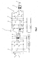
- the in Fig. 1 sketched inverter 1 is used to feed electrical energy from a DC power source 2, preferably a photovoltaic system 3, in a single-phase AC here 4.
- the inverter 1 has a DC / DC converter 5, which is applied between input lines 6 and 7 input DC voltage U E. converted into a DC output voltage U Z.
- the DC output voltage U Z is between output lines 8 and 9, which are also input lines of an inverter bridge 10 of the inverter 1, which feeds AC with the interposition of a sine wave filter 11 in the AC network 4.
- the inverter bridge 10 directs the DC output voltage U Z , which is also DC link DC voltage, into an AC output voltage.
- the inverter bridge 10 is formed here as an H5 circuit and has a total of five clocked switches V 1 to V 5 , which are driven in a basically known manner to feed starting from the DC output voltage U Z electrical energy in the AC network 4.
- the DC / DC converter 5 has a resonance circuit 12 having a resonance inductance L r1 and a resonance capacitance C r1 .
- On the input side of this resonant circuit 12 via two clocked switches S 1 and S 2 which freewheeling diodes can be connected in parallel, alternately connected to the input lines 6 and 7 of the inverter 1 electrically conductive.
- an alternating current return path 13 is provided, which is connected to the same lines 6 and 7 on the one hand and 8 and 9 on the other hand as the resonant circuit 12, and which allows the current flowing through the resonant circuit 12, to the DC source 2 to flow back.
- a capacitance C r2 is provided which, together with the resonance capacitance C r1, for a complete electrical isolation between the input lines 6 and 7 of the inverter 1 and the input lines 8 and 9 of the inverter bridge 10 provides.
- a resonance inductance L r2 is provided which configures the alternating current return path 13 as a further resonance circuit 14.
- the alternating current return path 13 is connected to the input lines 6 and 7 via two further clocked switches S 3 and S 4 , to which free-wheeling diodes can also be connected in parallel.
- the alternating current return path 13 is connected via rectifier diodes D 3 and D 4 to the input lines 8 and 9 of the inverter bridge 10.
- the AC return path 13 is formed in the same way as the resonant circuit 12.
- the switches S 1 and S 2 or S 3 and S 4 these two resonant circuits 12 and 14 are forced to antiphase oscillations.
- the alternating current return path is also connected to the input lines 6 and 7 at least on one side by clocked switches S 3 and S 4 , there is an additional possibility of influencing the total current flowing through the resonant circuit 12 and the alternating current return path 13.
- buffer capacitances C 1 and C 2 are provided between the input lines 6 and 7 and the input lines 8 and 9 buffer capacitances C 1 and C 2 are provided.
- the basic ratio of the inverter 1 between the DC input voltage U E and the DC output voltage U Z is 1: 1.
- the output DC voltage U Z can be acted upon in a highly variable manner.
- the resonant circuit 12 and the AC return paths 13 may be provided at this point a connection via an additional series circuit of capacitance and inductance, which positively influences the passive characteristics of the DC / DC converter 5.
- an additional series circuit of capacitance and inductance which positively influences the passive characteristics of the DC / DC converter 5.
- can also only one capacitor or only one inductor can be provided.
- the resonance inductance L r2 in the alternating current return path 13 is fundamentally optional.
- the switches S 1 to S 4 in the manner of an H5 circuit can be supplemented by a further switch in one of the input lines 6 and 7, which can also be clocked Tiefsetzstellend for the DC output voltage U Z.
- the embodiment of the inverter 1 according to Fig. 1 a variety of ways of influencing the DC output voltage U Z on.
- the DC / DC converter 5 may comprise two or more resonant circuits 12, which as such are identically formed of resonance inductors L r1 and resonant capacitances C r1 and are connected in parallel with each other, for example. B. are connected via rectifier diodes D 1 and D 2 to the output lines 8 and 9. Also the individual resonant circuits 12 then each associated AC return paths 13 can on the output side, that is connected in parallel to the output lines 8 and 9. However, it can also be closed together here and connected to the output line via common capacitances.
- the resonant circuits 12 and the associated alternating current return paths 13 are preferably not connected to both input lines 6 and 7 of the inverter 1, but via switches S 1 and S 2 to a maximum of one of the two input lines 6 and 7 and to a between the input lines 6 and 7 7 lying potential leading intermediate potential input line connected. At such intermediate potential input line is defined by capacitance intermediate potential. Accordingly, the inverter 1 then has a basic ratio of n: 1, where n is the number of parallel-connected resonant circuits 12.
- an auxiliary converter 17 is provided here to compensate for a current sum flowing through the resonant circuit 12 and the AC return path 13 so as not to provoke current over ground.
- the auxiliary converter has here two clocked switches S 7 and S 8 , with which a compensation current path 18 on the input side is alternately connected to the input lines 6 and 7.
- the compensation current path 18 runs parallel to the resonant circuit 12 and the alternating current return path 13.
- a connecting capacitor C e is arranged in it, via which it is connected here to the input line 9 of the inverter bridge 10.
- the AC return path 18 is connected via a coupling capacitance C K to the input line 7 grounded here, and in it is between the capacitances C e and C K on the one hand and the switches S 7 and S 8 on the other hand, an inductance L e provided.
- the capacitances C e and C K ensure the galvanic isolation along the compensation current path 18 as well.
- a controller 20 for the control of the clocked switches S 7 and S 8 of the auxiliary converter 17 controls the current flowing through the DC / DC converter 5 current sum to zero. With an annular core 19 and an induction coil not shown here as a summation current transformer, an input signal for the controller 20 is generated.
- the inverter 1 according to Fig. 2 is different than in Fig. 1 the Kompensationsstrompfad 18 with the auxiliary converter 17 via clocked switch S 9 and S 10 to the input lines 8 and 9 of the inverter bridge 10 connected. Accordingly, it has the inductance L e on the output side of the connection capacitance C e , and also the coupling capacitance C K is provided to the input line 9 of the inverter bridge 10 out.
- the compensation current path 18 is here directly connected to the input line 7.
- the controller 20 for the switches S 9 and S 10 essentially corresponds to the controller 20 for switches S 7 and S 8 according to FIG. 8, whereby here too only one of several possibilities is sketched for the execution of the controller 20.
- auxiliary converter 17 and a single compensation current path 18 are provided, although in principle also such a combination of auxiliary converter 17 and compensating current path 18 could be provided per pair of resonant circuit 12 and associated alternating current return path 13 to zero out each of the substream sums flowing over such a pair.
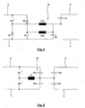
- Fig. 3 outlines an inverter 1, without here the DC power source 2 as in the Fig. 1 and 2 is reproduced. here are designated only the input poles DC + and DC - . The same applies to the alternating current network 4, for which the terminals L 1 and N are.
- the DC / DC converter 5 is provided here as SEPIC 15, which essentially comprises an input-side combination, an inductance L 1 and a switch S 1 , a coupling capacitor C k1 and an output-side inductance L 2 N 3 with a diode D 1 is constructed.
- the first special feature here is according to the teaching of EP 0 696 841 A1 Not only in the AC forward path 16, the coupling capacitor C k1 is provided, but also in the AC return path 13 has a coupling capacitance C k2 .
- an auxiliary converter 17 is provided which basically the same Structure has as the auxiliary converter 17 according to Fig. 1 Even if the coupling capacitance C k is connected to the input line 6 and the connection capacitor C e to the output line 8 here.
- the auxiliary transformer 4 for Erdstromkompensation in which the registered via the ferrite ring 19 current by driving the switches S 7 and S 8 is made to zero, this has no effect.
- Kompensationsstrompfad 18 is the jumper between the input lines 6 and 7 on two bridges from one of the switches S 7 and S 8 and a diode D. 7 or D 8 split. Accordingly, the inductance L e is divided into two partial inductances L e1 and L e2 . All other components of the compensation current path 18 correspond Fig. 1 except that the compensation current path 18 in Fig. 4 the output side is connected to the output line 8.
- the basic function of the compensation current path 18 according to Fig. 4 but corresponds to that according to Fig. 1 ,
- connection capacitance C e via which the compensation current path 18 is connected on the output side to the output lines 8 and 9, here is divided into two connection capacitances C e1 and C e2 , which the connection to a potential between the potentials of the output lines 8 and 9 with interposition of a Connection capacity corresponds. It is understood that the division of the two capacitances C K and C e can also be carried out independently of each other and that one or both of these corresponding divisions also in the other embodiments of the compensation current path 18 according to the Fig. 1 to 4 is possible.
Landscapes
- Engineering & Computer Science (AREA)
- Power Engineering (AREA)
- Dc-Dc Converters (AREA)
Claims (15)
- Convertisseur continu-continu (5) pour convertir une tension continue d'entrée (UE) appliquée entre deux lignes d'entrée (6 et 7) d'un côté d'entrée du convertisseur continu-continu (5) en une tension continue de sortie (UZ) appliquée entre deux lignes de sortie (8 et 9) d'un côté de sortie du convertisseur continu-continu (5), dans lequel le convertisseur continu-continu (5) comprenant:- au moins un trajet aller de courant alternatif (16), lequel est connecté, via des composants électriques, du côté d'entrée, aux lignes d'entrée (6 et 7) et du côté de sortie, aux lignes de sortie (8 et 9), dans lequel les composants électriques sont des composants électriques à commutation entre le trajet aller de courant alternatif (16) et au moins l'une des lignes d'entrée (6 et 7) et au moins l'une des lignes de sortie (8 et 9), l'un au moins d'entre eux étant commandé ; et- au moins un trajet de retour de courant alternatif (13) pour un retour d'un courant s'écoulant via le trajet aller de courant alternatif (16), lequel est relié, via des connexions, du côté d'entrée, à au moins l'une des lignes d'entrée (6 et 7) et du côté de sortie, à au moins l'une des lignes de sortie (8 et 9), dans lequel les connexions du côté d'entrée et du côté de sortie sont des connexions durablement électroconductrices ou des connexions à commutation électrique ;- dans lequel les lignes d'entrée (6 et 7) sont isolées de manière galvanique des lignes de sortie (8 et 9), par des condensateurs (Cr1, Cr2), dans tous les trajets de courant alternatif (16, 13),
caractérisé par- un convertisseur auxiliaire (17) pour compenser une somme de courants sur tous les trajets aller de courant alternatif (16) et trajets de retour de courant alternatif (13), lequel ne transmet pas plus de 10% du courant s'écoulant actuellement via tous les trajets aller de courant alternatif (16) et lequel relie de manière électroconductrice un trajet de courant de compensation (18) supplémentaire, lequel est connecté en parallèle aux tous les trajets aller de courant alternatif (16) et trajets de retour de courant alternatif (13), au niveau de l'une de ses extrémités, via deux commutateurs (S7, S8 respectivement S9, S10) commandés, alternativement à deux lignes sur le même côté du convertisseur continu-continu (5), lesquelles sont choisies dans le groupe de lignes comprenant :- les lignes d'entrée (6, 7),- des lignes d'entrée de potentiel intermédiaire, véhiculant des potentiels intermédiaires, situées entre les potentiels des lignes d'entrée,- les lignes de sortie (8 et 9) et- des lignes de sortie de potentiel intermédiaire, véhiculant des potentiels intermédiaires, situées entre les potentiels des lignes de sortie,
dans lequel le trajet de courant de compensation (18) est relié durablement de manière électroconductrice au niveau de son autre extrémité, via au moins un condensateur de liaison (Ce), à au moins une ligne située sur le côté en vis-à-vis du même côté du convertisseur continu-continu (5), laquelle est choisie dans le groupe de lignes. - Convertisseur continu-continu selon la revendication 1, dans lequel, dans le trajet de courant de compensation (18), une inductance (Le) est connectée en série avec le condensateur de liaison (Ce).
- Convertisseur continu-continu selon la revendication 1 ou 2, dans lequel le trajet de courant de compensation (18) est relié de manière électroconductrice au niveau d'un point entre le condensateur de liaison (Ce) et les commutateurs commandés (S7, S8; S9, S10), via un condensateur de couplage (CK), à l'une des deux lignes auxquelles le convertisseur auxiliaire (17) relie alternativement le trajet de courant de compensation (18) via les commutateurs commandés (S7, S8; S9, S10).
- Convertisseur continu-continu selon les revendications 2 et 3, dans lequel le point se situe entre le condensateur de liaison (Ce) et l'inductance (Le).
- Convertisseur continu-continu selon l'une des revendications 1 à 4, dans lequel une commande (20) du convertisseur auxiliaire (17) collecte une somme de courants sur tous les trajets aller de courant alternatif (16) et trajets retour de courant alternatif (13) ainsi que le trajet de courant de compensation (18), et la règle vers zéro.
- Convertisseur continu-continu selon la revendication 5, dans lequel la commande (20) assure la commande des commutateurs commandés (S7, S8; S9, S10) du convertisseur auxiliaire (17) avec une modulation des impulsions en largeur (PWM).
- Convertisseur continu-continu selon l'une des revendications 1 à 6, dans lequel le convertisseur continu-continu (5) comprend au moins un circuit résonant (12), présentant une inductance à résonance (Lr1) et un condensateur à résonance (Cr1), reprèsentant d'un trajet aller de courant alternatif (16), lequel est connecté du côté d'entrée, via au moins deux commutateurs commandés (S1 et S2), respectivement à l'une des deux lignes d'entrée (6 et 7).
- Convertisseur continu-continu selon l'une des revendications 1 à 7, dans lequel au moins un trajet de retour de courant alternatif (13) est relié, du côté d'entrée, aux lignes d'entrée (6 et 7) et du côté de sortie, aux lignes de sortie (8 et 9), dans lequel le condensateur (Cr2) est disposé dans le trajet de retour de courant alternatif (13) entre ses connexions du côté d'entrée aux lignes d'entrée (6 et 7) et ses connexions du côté de sortie aux deux lignes de sortie (8 et 9).
- Convertisseur continu-continu selon la revendication 7, dans lequel on associe à chaque circuit résonant (12) un trajet de retour de courant alternatif (13), lequel est relié du côté d'entrée et du côté de sortie aux mêmes lignes (6, 7, 8, 9) que celles auxquelles le circuit résonant (12) associé est connecté.
- Convertisseur continu-continu selon l'une des revendications 1 à 9, dans lequel on prévoit un trajet de retour de courant alternatif (13), lequel est relié, du côté d'entrée, aux lignes d'entrée (6 et 7) via deux condensateurs et du côté de sortie, aux lignes de sortie (8 et 9) via deux autres condensateurs.
- Convertisseur continu-continu selon l'une des revendications 1 à 9, dans lequel plusieurs trajets de retour de courant alternatif (13) sont reliés en commun, du côté de sortie, via deux condensateurs, aux lignes de sortie (8 et 9).
- Convertisseur continu-continu selon la revendication 7, dans lequel le trajet de retour de courant alternatif (13) est relié, via des connexions à commutation, du côté d'entrée, aux deux lignes d'entrée (6 et 7) et du côté de sortie, aux deux lignes de sortie (8 et 9), dans lequel les connexions à commutation comprennent, sur au moins un côté, des commutateurs commandés respectifs et dans lequel le trajet de retour de courant alternatif (13) est réalisé en tant qu'un autre circuit résonant (14) et présente, en plus du condensateur (Cr2), une inductance à résonance (Lr2).
- Convertisseur continu-continu selon la revendication 7 ou l'une des revendications précédentes faisant référence à la revendication 7, dans lequel chaque circuit résonant (12) et le trajet de retour de courant alternatif (13) qui lui est associé peuvent être reliés, au moins sur un côté du convertisseur continu-continu (5), via un commutateur de liaison commandé.
- Convertisseur continu-continu selon la revendication 7 ou l'une des revendications précédentes faisant référence à la revendication 7, caractérisé en ce que chaque circuit résonant (12) et le trajet de retour de courant alternatif (13) qui lui est associé sont reliés ensemble de manière électroconductrice, du côté de sortie, grâce à une connexion par couplage qui est choisie à partir d'un condensateur et d'une inductance.
- Convertisseur continu-continu selon la revendication 11, caractérisé en ce que chaque circuit résonant (12) et le trajet de retour de courant alternatif (13) qui lui est associé sont connectés du côté d'entrée, via respectivement deux commutateurs commandés (S1 et S2, S3 et S4), respectivement à l'une des deux lignes d'entrée (6 et 7), dans lequel, dans une ligne du côté d'entrée, laquelle est choisie à partir des lignes d'entrée (6 ou 7) et des lignes d'entrée de potentiel intermédiaire véhiculant des potentiels intermédiaires situées entre les lignes d'entrée, un autre commutateur commandé est disposé.
Priority Applications (1)
| Application Number | Priority Date | Filing Date | Title |
|---|---|---|---|
| EP10725772.7A EP2449664B1 (fr) | 2009-07-02 | 2010-06-22 | Convertisseur continu-continu avec convertisseur auxiliaire destiné à compenser le courant de fuite |
Applications Claiming Priority (3)
| Application Number | Priority Date | Filing Date | Title |
|---|---|---|---|
| EP09164447A EP2270966A1 (fr) | 2009-07-02 | 2009-07-02 | Convertisseur CC/CC doté d'un convertisseur auxiliaire pour la compensation du courant à la terre |
| PCT/EP2010/058817 WO2011000741A1 (fr) | 2009-07-02 | 2010-06-22 | Convertisseur continu-continu avec convertisseur auxiliaire destiné à compenser le courant de fuite |
| EP10725772.7A EP2449664B1 (fr) | 2009-07-02 | 2010-06-22 | Convertisseur continu-continu avec convertisseur auxiliaire destiné à compenser le courant de fuite |
Publications (2)
| Publication Number | Publication Date |
|---|---|
| EP2449664A1 EP2449664A1 (fr) | 2012-05-09 |
| EP2449664B1 true EP2449664B1 (fr) | 2015-08-26 |
Family
ID=41480091
Family Applications (2)
| Application Number | Title | Priority Date | Filing Date |
|---|---|---|---|
| EP09164447A Withdrawn EP2270966A1 (fr) | 2009-07-02 | 2009-07-02 | Convertisseur CC/CC doté d'un convertisseur auxiliaire pour la compensation du courant à la terre |
| EP10725772.7A Not-in-force EP2449664B1 (fr) | 2009-07-02 | 2010-06-22 | Convertisseur continu-continu avec convertisseur auxiliaire destiné à compenser le courant de fuite |
Family Applications Before (1)
| Application Number | Title | Priority Date | Filing Date |
|---|---|---|---|
| EP09164447A Withdrawn EP2270966A1 (fr) | 2009-07-02 | 2009-07-02 | Convertisseur CC/CC doté d'un convertisseur auxiliaire pour la compensation du courant à la terre |
Country Status (3)
| Country | Link |
|---|---|
| US (1) | US8587976B2 (fr) |
| EP (2) | EP2270966A1 (fr) |
| WO (1) | WO2011000741A1 (fr) |
Families Citing this family (6)
| Publication number | Priority date | Publication date | Assignee | Title |
|---|---|---|---|---|
| US9461538B2 (en) | 2013-09-23 | 2016-10-04 | Abb Technology Ltd | DC/DC converter |
| JP6176121B2 (ja) * | 2014-01-10 | 2017-08-09 | 住友電気工業株式会社 | 電力変換装置及び三相交流電源装置 |
| US10218275B2 (en) | 2016-08-02 | 2019-02-26 | Smart Prong Technologies, Inc. | Multi-stage voltage multiplication circuit for inverting a direct current power signal |
| DE102018205985A1 (de) | 2018-04-19 | 2019-10-24 | Audi Ag | Elektrisches Energiesystem mit Brennstoffzellen |
| FR3143236A1 (fr) * | 2022-12-07 | 2024-06-14 | Commissariat à l'énergie atomique et aux énergies alternatives | Dispositif électronique et procédé de pilotage d’un convertisseur d’énergie électrique, système électronique de conversion et programme d’ordinateur associés |
| CN117318454B (zh) * | 2023-11-28 | 2024-02-02 | 锦浪科技股份有限公司 | 一种低频共模漏电流抑制方法 |
Family Cites Families (12)
| Publication number | Priority date | Publication date | Assignee | Title |
|---|---|---|---|---|
| GB1506633A (en) | 1974-05-21 | 1978-04-05 | Senger N | Electrical isolating circuits |
| DE2508314C3 (de) * | 1975-02-24 | 1978-06-22 | Stellar Radiation, Variable Lichtemissionstechnik Norbert Senger, 6000 Frankfurt | Schaltungsanordnung zur galvanischen Trennung eines Verbrauchers von einem Speisenetz |
| US5134307A (en) * | 1989-05-18 | 1992-07-28 | Hirotami Nakano | Uninterruptible power supply apparatus and isolating method thereof |
| US5583421A (en) | 1994-08-10 | 1996-12-10 | Hewlett-Packard Company | Sepic converter with transformerless line isolation |
| US5784269A (en) * | 1997-02-21 | 1998-07-21 | Lucent Technologies, Inc. | Three phase high power factor converter using phase selection circuit |
| WO2001080411A1 (fr) * | 2000-04-12 | 2001-10-25 | Wolfgang Croce | Bloc d'alimentation secteur |
| CA2431689A1 (fr) * | 2003-06-16 | 2004-12-16 | Liu Canus | Convertisseur resonant commute au point d'intensite nulle du courant |
| TW200709544A (en) * | 2005-08-29 | 2007-03-01 | Ind Tech Res Inst | Transformer-free power conversion circuit for parallel connection with commercial electricity system |
| US7324356B2 (en) * | 2005-10-21 | 2008-01-29 | National Instruments Corporation | Common-mode current cancellation with digital pulses for isolated applications |
| EP2023475B1 (fr) | 2007-08-04 | 2016-10-12 | SMA Solar Technology AG | Inversion pour une source de tension continue reliée à la terre, en particulier un générateur photovoltaïque |
| ATE545190T1 (de) * | 2008-07-09 | 2012-02-15 | Sma Solar Technology Ag | Dc/dc-wandler |
| TW201246774A (en) * | 2011-05-02 | 2012-11-16 | Motech Ind Inc | Circuit for converting a direct current voltage to an alternating current voltage |
-
2009
- 2009-07-02 EP EP09164447A patent/EP2270966A1/fr not_active Withdrawn
-
2010
- 2010-06-22 WO PCT/EP2010/058817 patent/WO2011000741A1/fr not_active Ceased
- 2010-06-22 EP EP10725772.7A patent/EP2449664B1/fr not_active Not-in-force
-
2012
- 2012-01-03 US US13/342,343 patent/US8587976B2/en not_active Expired - Fee Related
Also Published As
| Publication number | Publication date |
|---|---|
| US8587976B2 (en) | 2013-11-19 |
| US20120113702A1 (en) | 2012-05-10 |
| EP2449664A1 (fr) | 2012-05-09 |
| EP2270966A1 (fr) | 2011-01-05 |
| WO2011000741A1 (fr) | 2011-01-06 |
Similar Documents
| Publication | Publication Date | Title |
|---|---|---|
| EP2377234B1 (fr) | Onduleur sans transformateur avec un convertisseur dc/dc | |
| EP2030299B1 (fr) | Onduleur destiné à injecter de l'énergie électrique dans un réseau de distribution d'énergie | |
| EP3840980B1 (fr) | Dispositif de charge avec tension centrale du circuit intermédiaire commandable et système d'entraînement avec tel dispositif de charge | |
| EP2023475B1 (fr) | Inversion pour une source de tension continue reliée à la terre, en particulier un générateur photovoltaïque | |
| DE102007038959A1 (de) | Wechselrichter | |
| EP2719051A2 (fr) | Convertisseur survolteur | |
| WO2013120784A2 (fr) | Dispositif d'alimentation réseau, système d'alimentation en énergie et procédé de fonctionnement d'un disposif d'alimentation réseau | |
| EP2852044B1 (fr) | Convertisseur bidirectionnel à direction préférentielle et onduleur capable de produire de la puissance reactive | |
| DE102006012164B4 (de) | Schaltungsanordnung zur Erzeugung einer Wechselspannung oder eines Wechselstroms | |
| EP2709257A2 (fr) | Circuit de convertisseur de courant et procédé de commande du circuit de convertisseur de courant | |
| DE102007038960A1 (de) | Wechselrichter | |
| EP2586646B1 (fr) | Dispositif électrique d'alimentation en énergie pour dispositifs d'entraînement destiné au fonctionnement d'un véhicule sur rail sur des réseaux d'alimentation électriques | |
| EP3257145B1 (fr) | Convertisseur cc/cc avec condensateur flottant | |
| WO2020064432A1 (fr) | Circuit de charge destiné à un accumulateur d'énergie électrique embarqué dans un véhicule | |
| EP2449664A1 (fr) | Convertisseur continu-continu avec convertisseur auxiliaire destiné à compenser le courant de fuite | |
| EP3785345B1 (fr) | Dispositif électronique de puissance à équipement de transformateur et procédé | |
| DE102013005277B3 (de) | Verfahren zum Umwandeln von Gleichspannung in Wechselspannung und Wechselrichterschaltung dafür | |
| DE102013102433A1 (de) | Wechselrichter für eine variable Eingangsgleichspannung | |
| DE102010060687A1 (de) | Leistungselektronische Wandlerstufe | |
| EP2339730A1 (fr) | Convertisseur CC/CC pouvant être relié à la terre | |
| DE102013208911A1 (de) | Mehrphasige Drossel mit integriertem Störungsunterdrückungstransformator | |
| EP0743744A2 (fr) | Convertisseur de courant | |
| DE102012206801A1 (de) | Schaltung mit einer stromrichterschaltung und verfahren zur leistungsanpassung | |
| EP3360241B1 (fr) | Convertisseur continu-continu et procédé de fonctionnement d'un convertisseur continu-continu | |
| EP3518401A1 (fr) | Convertisseur hybride triphasé |
Legal Events
| Date | Code | Title | Description |
|---|---|---|---|
| PUAI | Public reference made under article 153(3) epc to a published international application that has entered the european phase |
Free format text: ORIGINAL CODE: 0009012 |
|
| 17P | Request for examination filed |
Effective date: 20120126 |
|
| AK | Designated contracting states |
Kind code of ref document: A1 Designated state(s): AL AT BE BG CH CY CZ DE DK EE ES FI FR GB GR HR HU IE IS IT LI LT LU LV MC MK MT NL NO PL PT RO SE SI SK SM TR |
|
| DAX | Request for extension of the european patent (deleted) | ||
| GRAP | Despatch of communication of intention to grant a patent |
Free format text: ORIGINAL CODE: EPIDOSNIGR1 |
|
| INTG | Intention to grant announced |
Effective date: 20150421 |
|
| GRAS | Grant fee paid |
Free format text: ORIGINAL CODE: EPIDOSNIGR3 |
|
| GRAA | (expected) grant |
Free format text: ORIGINAL CODE: 0009210 |
|
| AK | Designated contracting states |
Kind code of ref document: B1 Designated state(s): AL AT BE BG CH CY CZ DE DK EE ES FI FR GB GR HR HU IE IS IT LI LT LU LV MC MK MT NL NO PL PT RO SE SI SK SM TR |
|
| REG | Reference to a national code |
Ref country code: GB Ref legal event code: FG4D Free format text: NOT ENGLISH |
|
| REG | Reference to a national code |
Ref country code: CH Ref legal event code: EP |
|
| REG | Reference to a national code |
Ref country code: AT Ref legal event code: REF Ref document number: 745701 Country of ref document: AT Kind code of ref document: T Effective date: 20150915 |
|
| REG | Reference to a national code |
Ref country code: IE Ref legal event code: FG4D Free format text: LANGUAGE OF EP DOCUMENT: GERMAN |
|
| REG | Reference to a national code |
Ref country code: DE Ref legal event code: R096 Ref document number: 502010010163 Country of ref document: DE |
|
| REG | Reference to a national code |
Ref country code: LT Ref legal event code: MG4D |
|
| PG25 | Lapsed in a contracting state [announced via postgrant information from national office to epo] |
Ref country code: LT Free format text: LAPSE BECAUSE OF FAILURE TO SUBMIT A TRANSLATION OF THE DESCRIPTION OR TO PAY THE FEE WITHIN THE PRESCRIBED TIME-LIMIT Effective date: 20150826 Ref country code: FI Free format text: LAPSE BECAUSE OF FAILURE TO SUBMIT A TRANSLATION OF THE DESCRIPTION OR TO PAY THE FEE WITHIN THE PRESCRIBED TIME-LIMIT Effective date: 20150826 Ref country code: LV Free format text: LAPSE BECAUSE OF FAILURE TO SUBMIT A TRANSLATION OF THE DESCRIPTION OR TO PAY THE FEE WITHIN THE PRESCRIBED TIME-LIMIT Effective date: 20150826 Ref country code: NO Free format text: LAPSE BECAUSE OF FAILURE TO SUBMIT A TRANSLATION OF THE DESCRIPTION OR TO PAY THE FEE WITHIN THE PRESCRIBED TIME-LIMIT Effective date: 20151126 Ref country code: GR Free format text: LAPSE BECAUSE OF FAILURE TO SUBMIT A TRANSLATION OF THE DESCRIPTION OR TO PAY THE FEE WITHIN THE PRESCRIBED TIME-LIMIT Effective date: 20151127 |
|
| REG | Reference to a national code |
Ref country code: NL Ref legal event code: MP Effective date: 20150826 |
|
| PG25 | Lapsed in a contracting state [announced via postgrant information from national office to epo] |
Ref country code: HR Free format text: LAPSE BECAUSE OF FAILURE TO SUBMIT A TRANSLATION OF THE DESCRIPTION OR TO PAY THE FEE WITHIN THE PRESCRIBED TIME-LIMIT Effective date: 20150826 Ref country code: PT Free format text: LAPSE BECAUSE OF FAILURE TO SUBMIT A TRANSLATION OF THE DESCRIPTION OR TO PAY THE FEE WITHIN THE PRESCRIBED TIME-LIMIT Effective date: 20151228 Ref country code: IS Free format text: LAPSE BECAUSE OF FAILURE TO SUBMIT A TRANSLATION OF THE DESCRIPTION OR TO PAY THE FEE WITHIN THE PRESCRIBED TIME-LIMIT Effective date: 20151226 Ref country code: PL Free format text: LAPSE BECAUSE OF FAILURE TO SUBMIT A TRANSLATION OF THE DESCRIPTION OR TO PAY THE FEE WITHIN THE PRESCRIBED TIME-LIMIT Effective date: 20150826 Ref country code: ES Free format text: LAPSE BECAUSE OF FAILURE TO SUBMIT A TRANSLATION OF THE DESCRIPTION OR TO PAY THE FEE WITHIN THE PRESCRIBED TIME-LIMIT Effective date: 20150826 Ref country code: SE Free format text: LAPSE BECAUSE OF FAILURE TO SUBMIT A TRANSLATION OF THE DESCRIPTION OR TO PAY THE FEE WITHIN THE PRESCRIBED TIME-LIMIT Effective date: 20150826 |
|
| PG25 | Lapsed in a contracting state [announced via postgrant information from national office to epo] |
Ref country code: NL Free format text: LAPSE BECAUSE OF FAILURE TO SUBMIT A TRANSLATION OF THE DESCRIPTION OR TO PAY THE FEE WITHIN THE PRESCRIBED TIME-LIMIT Effective date: 20150826 |
|
| PG25 | Lapsed in a contracting state [announced via postgrant information from national office to epo] |
Ref country code: EE Free format text: LAPSE BECAUSE OF FAILURE TO SUBMIT A TRANSLATION OF THE DESCRIPTION OR TO PAY THE FEE WITHIN THE PRESCRIBED TIME-LIMIT Effective date: 20150826 Ref country code: SK Free format text: LAPSE BECAUSE OF FAILURE TO SUBMIT A TRANSLATION OF THE DESCRIPTION OR TO PAY THE FEE WITHIN THE PRESCRIBED TIME-LIMIT Effective date: 20150826 Ref country code: IT Free format text: LAPSE BECAUSE OF FAILURE TO SUBMIT A TRANSLATION OF THE DESCRIPTION OR TO PAY THE FEE WITHIN THE PRESCRIBED TIME-LIMIT Effective date: 20150826 Ref country code: DK Free format text: LAPSE BECAUSE OF FAILURE TO SUBMIT A TRANSLATION OF THE DESCRIPTION OR TO PAY THE FEE WITHIN THE PRESCRIBED TIME-LIMIT Effective date: 20150826 Ref country code: CZ Free format text: LAPSE BECAUSE OF FAILURE TO SUBMIT A TRANSLATION OF THE DESCRIPTION OR TO PAY THE FEE WITHIN THE PRESCRIBED TIME-LIMIT Effective date: 20150826 |
|
| REG | Reference to a national code |
Ref country code: DE Ref legal event code: R097 Ref document number: 502010010163 Country of ref document: DE |
|
| PG25 | Lapsed in a contracting state [announced via postgrant information from national office to epo] |
Ref country code: RO Free format text: LAPSE BECAUSE OF FAILURE TO SUBMIT A TRANSLATION OF THE DESCRIPTION OR TO PAY THE FEE WITHIN THE PRESCRIBED TIME-LIMIT Effective date: 20150826 |
|
| REG | Reference to a national code |
Ref country code: FR Ref legal event code: PLFP Year of fee payment: 7 |
|
| PLBE | No opposition filed within time limit |
Free format text: ORIGINAL CODE: 0009261 |
|
| STAA | Information on the status of an ep patent application or granted ep patent |
Free format text: STATUS: NO OPPOSITION FILED WITHIN TIME LIMIT |
|
| 26N | No opposition filed |
Effective date: 20160530 |
|
| PG25 | Lapsed in a contracting state [announced via postgrant information from national office to epo] |
Ref country code: SI Free format text: LAPSE BECAUSE OF FAILURE TO SUBMIT A TRANSLATION OF THE DESCRIPTION OR TO PAY THE FEE WITHIN THE PRESCRIBED TIME-LIMIT Effective date: 20150826 |
|
| PG25 | Lapsed in a contracting state [announced via postgrant information from national office to epo] |
Ref country code: BE Free format text: LAPSE BECAUSE OF NON-PAYMENT OF DUE FEES Effective date: 20160630 |
|
| PG25 | Lapsed in a contracting state [announced via postgrant information from national office to epo] |
Ref country code: MC Free format text: LAPSE BECAUSE OF FAILURE TO SUBMIT A TRANSLATION OF THE DESCRIPTION OR TO PAY THE FEE WITHIN THE PRESCRIBED TIME-LIMIT Effective date: 20150826 |
|
| REG | Reference to a national code |
Ref country code: CH Ref legal event code: PL |
|
| REG | Reference to a national code |
Ref country code: IE Ref legal event code: MM4A |
|
| PG25 | Lapsed in a contracting state [announced via postgrant information from national office to epo] |
Ref country code: CH Free format text: LAPSE BECAUSE OF NON-PAYMENT OF DUE FEES Effective date: 20160630 Ref country code: LI Free format text: LAPSE BECAUSE OF NON-PAYMENT OF DUE FEES Effective date: 20160630 |
|
| PG25 | Lapsed in a contracting state [announced via postgrant information from national office to epo] |
Ref country code: IE Free format text: LAPSE BECAUSE OF NON-PAYMENT OF DUE FEES Effective date: 20160622 |
|
| REG | Reference to a national code |
Ref country code: FR Ref legal event code: PLFP Year of fee payment: 8 |
|
| REG | Reference to a national code |
Ref country code: AT Ref legal event code: MM01 Ref document number: 745701 Country of ref document: AT Kind code of ref document: T Effective date: 20160622 |
|
| PG25 | Lapsed in a contracting state [announced via postgrant information from national office to epo] |
Ref country code: AT Free format text: LAPSE BECAUSE OF NON-PAYMENT OF DUE FEES Effective date: 20160622 |
|
| PG25 | Lapsed in a contracting state [announced via postgrant information from national office to epo] |
Ref country code: SM Free format text: LAPSE BECAUSE OF FAILURE TO SUBMIT A TRANSLATION OF THE DESCRIPTION OR TO PAY THE FEE WITHIN THE PRESCRIBED TIME-LIMIT Effective date: 20150826 Ref country code: HU Free format text: LAPSE BECAUSE OF FAILURE TO SUBMIT A TRANSLATION OF THE DESCRIPTION OR TO PAY THE FEE WITHIN THE PRESCRIBED TIME-LIMIT; INVALID AB INITIO Effective date: 20100622 Ref country code: CY Free format text: LAPSE BECAUSE OF FAILURE TO SUBMIT A TRANSLATION OF THE DESCRIPTION OR TO PAY THE FEE WITHIN THE PRESCRIBED TIME-LIMIT Effective date: 20150826 |
|
| REG | Reference to a national code |
Ref country code: FR Ref legal event code: PLFP Year of fee payment: 9 |
|
| PG25 | Lapsed in a contracting state [announced via postgrant information from national office to epo] |
Ref country code: MT Free format text: LAPSE BECAUSE OF FAILURE TO SUBMIT A TRANSLATION OF THE DESCRIPTION OR TO PAY THE FEE WITHIN THE PRESCRIBED TIME-LIMIT Effective date: 20150826 Ref country code: MK Free format text: LAPSE BECAUSE OF FAILURE TO SUBMIT A TRANSLATION OF THE DESCRIPTION OR TO PAY THE FEE WITHIN THE PRESCRIBED TIME-LIMIT Effective date: 20150826 Ref country code: LU Free format text: LAPSE BECAUSE OF NON-PAYMENT OF DUE FEES Effective date: 20160622 Ref country code: TR Free format text: LAPSE BECAUSE OF FAILURE TO SUBMIT A TRANSLATION OF THE DESCRIPTION OR TO PAY THE FEE WITHIN THE PRESCRIBED TIME-LIMIT Effective date: 20150826 |
|
| PG25 | Lapsed in a contracting state [announced via postgrant information from national office to epo] |
Ref country code: BG Free format text: LAPSE BECAUSE OF FAILURE TO SUBMIT A TRANSLATION OF THE DESCRIPTION OR TO PAY THE FEE WITHIN THE PRESCRIBED TIME-LIMIT Effective date: 20150826 |
|
| PG25 | Lapsed in a contracting state [announced via postgrant information from national office to epo] |
Ref country code: AL Free format text: LAPSE BECAUSE OF FAILURE TO SUBMIT A TRANSLATION OF THE DESCRIPTION OR TO PAY THE FEE WITHIN THE PRESCRIBED TIME-LIMIT Effective date: 20150826 |
|
| PGFP | Annual fee paid to national office [announced via postgrant information from national office to epo] |
Ref country code: DE Payment date: 20200623 Year of fee payment: 11 Ref country code: FR Payment date: 20200623 Year of fee payment: 11 |
|
| PGFP | Annual fee paid to national office [announced via postgrant information from national office to epo] |
Ref country code: GB Payment date: 20200625 Year of fee payment: 11 |
|
| REG | Reference to a national code |
Ref country code: DE Ref legal event code: R119 Ref document number: 502010010163 Country of ref document: DE |
|
| GBPC | Gb: european patent ceased through non-payment of renewal fee |
Effective date: 20210622 |
|
| PG25 | Lapsed in a contracting state [announced via postgrant information from national office to epo] |
Ref country code: GB Free format text: LAPSE BECAUSE OF NON-PAYMENT OF DUE FEES Effective date: 20210622 Ref country code: DE Free format text: LAPSE BECAUSE OF NON-PAYMENT OF DUE FEES Effective date: 20220101 |
|
| PG25 | Lapsed in a contracting state [announced via postgrant information from national office to epo] |
Ref country code: FR Free format text: LAPSE BECAUSE OF NON-PAYMENT OF DUE FEES Effective date: 20210630 |