EP2450923A2 - Système de condensateur et procédé de fabrication d'un système de condensateur - Google Patents
Système de condensateur et procédé de fabrication d'un système de condensateur Download PDFInfo
- Publication number
- EP2450923A2 EP2450923A2 EP20110185535 EP11185535A EP2450923A2 EP 2450923 A2 EP2450923 A2 EP 2450923A2 EP 20110185535 EP20110185535 EP 20110185535 EP 11185535 A EP11185535 A EP 11185535A EP 2450923 A2 EP2450923 A2 EP 2450923A2
- Authority
- EP
- European Patent Office
- Prior art keywords
- capacitor
- spacer
- metal
- shaped body
- recess
- Prior art date
- Legal status (The legal status is an assumption and is not a legal conclusion. Google has not performed a legal analysis and makes no representation as to the accuracy of the status listed.)
- Withdrawn
Links
- 238000000034 method Methods 0.000 title claims 7
- 238000004519 manufacturing process Methods 0.000 title description 8
- 239000003990 capacitor Substances 0.000 claims description 162
- 239000002184 metal Substances 0.000 claims description 92
- 125000006850 spacer group Chemical group 0.000 claims description 57
- 239000004065 semiconductor Substances 0.000 claims description 54
- 239000000463 material Substances 0.000 claims description 47
- 238000004382 potting Methods 0.000 claims description 47
- 238000000465 moulding Methods 0.000 claims description 39
- 239000012777 electrically insulating material Substances 0.000 claims description 8
- 238000003475 lamination Methods 0.000 claims description 5
- 230000004308 accommodation Effects 0.000 claims 1
- 238000010438 heat treatment Methods 0.000 abstract 2
- 238000001035 drying Methods 0.000 abstract 1
- 239000007788 liquid Substances 0.000 description 24
- 238000001816 cooling Methods 0.000 description 9
- 239000000110 cooling liquid Substances 0.000 description 8
- 238000010292 electrical insulation Methods 0.000 description 5
- 238000002347 injection Methods 0.000 description 3
- 239000007924 injection Substances 0.000 description 3
- 238000006243 chemical reaction Methods 0.000 description 2
- 150000001875 compounds Chemical class 0.000 description 2
- 238000010276 construction Methods 0.000 description 2
- 239000002985 plastic film Substances 0.000 description 2
- 229920006255 plastic film Polymers 0.000 description 2
- 239000002918 waste heat Substances 0.000 description 2
- 238000003466 welding Methods 0.000 description 2
- 238000005266 casting Methods 0.000 description 1
- 239000003989 dielectric material Substances 0.000 description 1
- 238000006073 displacement reaction Methods 0.000 description 1
- 238000005538 encapsulation Methods 0.000 description 1
- 238000009434 installation Methods 0.000 description 1
- 239000007769 metal material Substances 0.000 description 1
- 239000004033 plastic Substances 0.000 description 1
- 239000000376 reactant Substances 0.000 description 1
- 239000007787 solid Substances 0.000 description 1
- 239000000126 substance Substances 0.000 description 1
- 230000009466 transformation Effects 0.000 description 1
- 238000007740 vapor deposition Methods 0.000 description 1
Images

Classifications
-
- H—ELECTRICITY
- H01—ELECTRIC ELEMENTS
- H01G—CAPACITORS; CAPACITORS, RECTIFIERS, DETECTORS, SWITCHING DEVICES, LIGHT-SENSITIVE OR TEMPERATURE-SENSITIVE DEVICES OF THE ELECTROLYTIC TYPE
- H01G2/00—Details of capacitors not covered by a single one of groups H01G4/00-H01G11/00
- H01G2/08—Cooling arrangements; Heating arrangements; Ventilating arrangements
-
- H—ELECTRICITY
- H01—ELECTRIC ELEMENTS
- H01G—CAPACITORS; CAPACITORS, RECTIFIERS, DETECTORS, SWITCHING DEVICES, LIGHT-SENSITIVE OR TEMPERATURE-SENSITIVE DEVICES OF THE ELECTROLYTIC TYPE
- H01G4/00—Fixed capacitors; Processes of their manufacture
- H01G4/002—Details
- H01G4/005—Electrodes
- H01G4/008—Selection of materials
-
- H—ELECTRICITY
- H01—ELECTRIC ELEMENTS
- H01G—CAPACITORS; CAPACITORS, RECTIFIERS, DETECTORS, SWITCHING DEVICES, LIGHT-SENSITIVE OR TEMPERATURE-SENSITIVE DEVICES OF THE ELECTROLYTIC TYPE
- H01G2/00—Details of capacitors not covered by a single one of groups H01G4/00-H01G11/00
- H01G2/02—Mountings
-
- H—ELECTRICITY
- H01—ELECTRIC ELEMENTS
- H01G—CAPACITORS; CAPACITORS, RECTIFIERS, DETECTORS, SWITCHING DEVICES, LIGHT-SENSITIVE OR TEMPERATURE-SENSITIVE DEVICES OF THE ELECTROLYTIC TYPE
- H01G2/00—Details of capacitors not covered by a single one of groups H01G4/00-H01G11/00
- H01G2/10—Housing; Encapsulation
- H01G2/106—Fixing the capacitor in a housing
-
- H—ELECTRICITY
- H01—ELECTRIC ELEMENTS
- H01G—CAPACITORS; CAPACITORS, RECTIFIERS, DETECTORS, SWITCHING DEVICES, LIGHT-SENSITIVE OR TEMPERATURE-SENSITIVE DEVICES OF THE ELECTROLYTIC TYPE
- H01G4/00—Fixed capacitors; Processes of their manufacture
- H01G4/002—Details
- H01G4/224—Housing; Encapsulation
-
- H—ELECTRICITY
- H01—ELECTRIC ELEMENTS
- H01G—CAPACITORS; CAPACITORS, RECTIFIERS, DETECTORS, SWITCHING DEVICES, LIGHT-SENSITIVE OR TEMPERATURE-SENSITIVE DEVICES OF THE ELECTROLYTIC TYPE
- H01G9/00—Electrolytic capacitors, rectifiers, detectors, switching devices, light-sensitive or temperature-sensitive devices; Processes of their manufacture
- H01G9/004—Details
- H01G9/008—Terminals
-
- H—ELECTRICITY
- H05—ELECTRIC TECHNIQUES NOT OTHERWISE PROVIDED FOR
- H05K—PRINTED CIRCUITS; CASINGS OR CONSTRUCTIONAL DETAILS OF ELECTRIC APPARATUS; MANUFACTURE OF ASSEMBLAGES OF ELECTRICAL COMPONENTS
- H05K7/00—Constructional details common to different types of electric apparatus
- H05K7/20—Modifications to facilitate cooling, ventilating, or heating
- H05K7/2089—Modifications to facilitate cooling, ventilating, or heating for power electronics, e.g. for inverters for controlling motor
- H05K7/20927—Liquid coolant without phase change
-
- H—ELECTRICITY
- H10—SEMICONDUCTOR DEVICES; ELECTRIC SOLID-STATE DEVICES NOT OTHERWISE PROVIDED FOR
- H10D—INORGANIC ELECTRIC SEMICONDUCTOR DEVICES
- H10D1/00—Resistors, capacitors or inductors
- H10D1/60—Capacitors
- H10D1/68—Capacitors having no potential barriers
-
- Y—GENERAL TAGGING OF NEW TECHNOLOGICAL DEVELOPMENTS; GENERAL TAGGING OF CROSS-SECTIONAL TECHNOLOGIES SPANNING OVER SEVERAL SECTIONS OF THE IPC; TECHNICAL SUBJECTS COVERED BY FORMER USPC CROSS-REFERENCE ART COLLECTIONS [XRACs] AND DIGESTS
- Y10—TECHNICAL SUBJECTS COVERED BY FORMER USPC
- Y10T—TECHNICAL SUBJECTS COVERED BY FORMER US CLASSIFICATION
- Y10T29/00—Metal working
- Y10T29/43—Electric condenser making
Definitions
- the capacitor system has a metal mold body having a depression, a capacitor arranged at least partially in the depression and an electrically insulating potting material provided in the depression, which arranges the capacitor in the depression such that the capacitor does not touch the metal mold body and thus electrically therefrom is isolated.
- the metal mold body promotes the removal of heat that develops in the condenser.
- this metal molding could also consist of a comparatively robust and heat-conductive non-metallic material.
- the introduction of the liquid potting material between the condenser and the metal moldings can be carried out by introducing the potting material into the recess in front of the condenser.
- the potting material is displaced by the capacitor when introducing the capacitor into the recess so that the potting material, the space between the capacitor and metal moldings partially preferred but complete, i. according to the amount of potting material, fills.
- This introduction of the liquid potting material between the condenser and metal moldings can also take place in that the potting material is also poured into the recess in the space between the condenser and metal moldings after introduction of the capacitor into the cavity, injected under pressure or sucked into it by means of vacuum.
- At least one corresponding injection opening may be provided in a side wall of the depression.
- the potting material is pressed due to the applied pressure between the capacitor and the metal moldings, even if the distance between the capacitor and metal moldings low or, for example, measured at the to be reached by the potting material between capacitor and metal moldings dielectric strength is minimal.
- the dimensions of the recess and thus the distance between the condenser and metal moldings are to be dimensioned such that both a to be reached by the potting material between the capacitor and metal moldings Dielectric strength and achieved by the potting material between the capacitor and metal mold body heat transfer is achieved.
- FIG. 4 a schematic cross section through a metal shaped body for a capacitor module according to the embodiment according to FIG. 1 ;
- FIG. 5 a schematic exploded view of a capacitor module according to the embodiment according to FIG. 1 ,
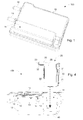
- FIG. 1 shows a perspective view of the underside of a metal shaped body 10 for a capacitor module 100 according to a first embodiment, the individual elements of which deviate from the drawings also as described above Design can accept.
- the metal shaped body 10 shown has a recess 11 which is adapted to receive a in the FIG. 1 not shown capacitor 20 is formed.
- the metal molding 10 is formed as a liquid-cooled heat sink and has to guide the cooling liquid to a liquid inlet 12 and a liquid outlet 13.
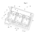
- FIG. 12 shows a first perspective view of the upper side of the metal shaped body 10 for a capacitor module 100 according to the embodiment FIG. 1 wherein the capacitor module 100 forms part of a power semiconductor module 200.
- power semiconductor circuits 210 are arranged on the shaped metal body 10 such that the shaped metal body 10 functions as a cooling body for the power semiconductor circuits 210.
- the power semiconductor circuits 210 have first terminals 211 through which a direct electrical contact to those in the FIG. 2 not shown, respective contacts 23, 24 of the in the FIG. 2 also not shown capacitor 20 can be produced.
- the power semiconductor circuits 210 also have second terminals 212 formed here as an AC voltage terminal.
- FIGS. 1 and 2 show the FIG. 3 a liquid inlet 12 and a liquid outlet 13 for guiding a cooling liquid for cooling the metal shaped body 10.
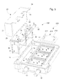
- FIG. 5 FIG. 12 is a schematic exploded view of a capacitor module 100 according to the embodiment FIG. 1 wherein the capacitor module 100 forms part of a power semiconductor module 200.
- the capacitor module 100 has a shaped metal body 10, a capacitor 20 and a spacer 30 made of an electrically insulating material.
- power semiconductor circuits 210 of the power semiconductor module 200 may be disposed on the metal mold 10 such that the metal mold 10 functions as a heat sink for the power semiconductor circuits 210.
- a cooling liquid which is supplied to the metal shaped body 10 via a liquid inlet 12, via a not shown, the first liquid line connected to the liquid inlet 12 inlet opening 14 flow into a cavity 15 of the metal mold body 10 and via a, not shown, second liquid line connected to the liquid outlet 13 Outlet 16 to flow out of the cavity 15 of the metal molding 10 again.
- the capacitor 20 has at least two metallic contact electrodes 21, 22 and a stack-up 25 of at least two electrodes and a dielectric.
- the contact electrodes 21, 22 form part of the outer surface of the capacitor 20.
- a tongue-shaped portion of the respective contact electrode 21, 22 serves as a capacitor terminal 23, 24th
- the spacer 30 is formed as a hollow body for accurately fitting receiving the capacitor 20. A majority of the outer walls of the spacer 30 is opened through openings 31. The spacer 30 thus has a corresponding basket-like shape. At an upper edge of the spacer 30, optional protrusions 32 are provided. The protrusions 32 may serve to electrically isolate current-carrying lines extending between the respective capacitor terminals 23, 24 and the respective terminals 211 of the power semiconductor circuits 210 from the metal mold 10. The fact that the projections 32 are provided on the spacer 30 and thus do not have to be mounted as separate elements on the metal molding simplifies the assembly of the power semiconductor module 200.
Landscapes
- Engineering & Computer Science (AREA)
- Power Engineering (AREA)
- Microelectronics & Electronic Packaging (AREA)
- Manufacturing & Machinery (AREA)
- Physics & Mathematics (AREA)
- Thermal Sciences (AREA)
- Chemical & Material Sciences (AREA)
- Materials Engineering (AREA)
- Inverter Devices (AREA)
- Fixed Capacitors And Capacitor Manufacturing Machines (AREA)
- Cooling Or The Like Of Electrical Apparatus (AREA)
- Cooling Or The Like Of Semiconductors Or Solid State Devices (AREA)
- Semiconductor Integrated Circuits (AREA)
Applications Claiming Priority (1)
| Application Number | Priority Date | Filing Date | Title |
|---|---|---|---|
| DE102010043445A DE102010043445B3 (de) | 2010-11-05 | 2010-11-05 | Kondensatoranordnung, leistungselektronisches Gerät damit undVerfahren zur Herstellung der Kondensatoranordnung |
Publications (2)
| Publication Number | Publication Date |
|---|---|
| EP2450923A2 true EP2450923A2 (fr) | 2012-05-09 |
| EP2450923A3 EP2450923A3 (fr) | 2015-09-02 |
Family
ID=45896056
Family Applications (1)
| Application Number | Title | Priority Date | Filing Date |
|---|---|---|---|
| EP11185535.9A Withdrawn EP2450923A3 (fr) | 2010-11-05 | 2011-10-18 | Système de condensateur et procédé de fabrication d'un système de condensateur |
Country Status (6)
| Country | Link |
|---|---|
| US (1) | US9058932B2 (fr) |
| EP (1) | EP2450923A3 (fr) |
| KR (1) | KR101865927B1 (fr) |
| CN (1) | CN102543423B (fr) |
| BR (1) | BRPI1106640A2 (fr) |
| DE (1) | DE102010043445B3 (fr) |
Families Citing this family (21)
| Publication number | Priority date | Publication date | Assignee | Title |
|---|---|---|---|---|
| JP5914290B2 (ja) * | 2012-10-15 | 2016-05-11 | 日立オートモティブシステムズ株式会社 | 電力変換装置 |
| KR20140078506A (ko) * | 2012-12-17 | 2014-06-25 | 엘에스산전 주식회사 | Dc 링크 커패시터 어셈블리 |
| JP2015082951A (ja) * | 2013-10-24 | 2015-04-27 | トヨタ自動車株式会社 | 電力変換装置 |
| CN104682722B (zh) * | 2013-11-26 | 2018-01-26 | 台达电子企业管理(上海)有限公司 | 电源转换装置及其组装方法 |
| US9615490B2 (en) * | 2014-05-15 | 2017-04-04 | Lear Corporation | Coldplate with integrated DC link capacitor for cooling thereof |
| GB2542468B (en) * | 2015-07-22 | 2017-12-13 | Lear Corp | Coldplate with integrated DC link capacitor for cooling thereof |
| DE102015214308A1 (de) * | 2015-07-29 | 2016-10-27 | Conti Temic Microelectronic Gmbh | Kühlvorrichtung, Leistungselektronikanordnung mit einer Kühlvorrichtung |
| US10490469B2 (en) * | 2015-10-28 | 2019-11-26 | Mitsubishi Electric Corporation | Power converting device |
| FR3043880B1 (fr) * | 2015-11-13 | 2017-12-29 | Valeo Systemes De Controle Moteur | Boitier pour un equipement electrique |
| JP6521850B2 (ja) * | 2015-12-08 | 2019-05-29 | 三菱重工サーマルシステムズ株式会社 | コンデンサユニット及び電力変換装置 |
| DK3206468T3 (en) * | 2016-02-15 | 2019-04-01 | Siemens Ag | DC converter with DC voltage |
| WO2017221230A1 (fr) * | 2016-06-23 | 2017-12-28 | Celem Passive Components Ltd | Système de montage de condensateur sur dispositif de refroidissement |
| EP3525221B1 (fr) * | 2016-11-11 | 2022-10-12 | NSK Ltd. | Dispositif de commande électronique et dispositif de direction |
| FR3104890B1 (fr) * | 2019-12-12 | 2022-06-24 | Valeo Siemens Eautomotive France Sas | Module d’isolation électrique pour équipement électrique haute tension |
| JP6921282B1 (ja) * | 2020-07-17 | 2021-08-18 | 三菱電機株式会社 | 電力変換装置 |
| US11889666B2 (en) * | 2021-11-03 | 2024-01-30 | Toyota Motor Engineering & Manufacturing North America, Inc. | Power device assemblies having embedded PCBs and methods of fabricating the same |
| US11997838B2 (en) * | 2022-02-01 | 2024-05-28 | Toyota Motor Engineering & Manufacturing North America, Inc. | Power device assemblies and methods of fabricating the same |
| DE102022203036A1 (de) | 2022-03-28 | 2023-09-28 | Valeo Eautomotive Germany Gmbh | Zwischenkreiskondensator für ein elektrisches Modul und einen Stromrichter mit verbesserter Kühlung sowie elektrisches Modul, Stromrichter und Elektrofahrzeug dazu |
| JP7809017B2 (ja) * | 2022-06-02 | 2026-01-30 | 三菱電機株式会社 | 電力変換装置 |
| KR20240030454A (ko) | 2022-08-30 | 2024-03-07 | 엘지이노텍 주식회사 | 커패시터 모듈 및 인버터 모듈 |
| DE102023211385A1 (de) * | 2023-11-16 | 2025-05-22 | Zf Friedrichshafen Ag | Kondensator, insbesondere Zwischenkreiskondensator, für eine Leistungselektronik eines Fahrzeugs |
Citations (1)
| Publication number | Priority date | Publication date | Assignee | Title |
|---|---|---|---|---|
| EP0994494A1 (fr) | 1998-10-13 | 2000-04-19 | Semikron Elektronik GmbH | Condensateur à basse inductance pour montage sur circuits intermédiaires |
Family Cites Families (20)
| Publication number | Priority date | Publication date | Assignee | Title |
|---|---|---|---|---|
| US3551756A (en) * | 1968-11-06 | 1970-12-29 | Cornell Dubilier Electric | Electrolytic capacitors with mechanically stabilized electrode assembly |
| JPS496446A (fr) * | 1972-05-09 | 1974-01-21 | ||
| JP2536657B2 (ja) * | 1990-03-28 | 1996-09-18 | 三菱電機株式会社 | 電気装置及びその製造方法 |
| KR940002697A (ko) * | 1992-07-13 | 1994-02-19 | 시모야마 도시로오 | 바 코드 주사 스티치 |
| DE9312006U1 (de) * | 1993-08-11 | 1993-09-23 | Fischer, Gerhard, 91052 Erlangen | Kondensatoranordnung fuer hochleistungs- und hochfrequenzanwendungen |
| DE19817493C1 (de) * | 1998-04-20 | 1999-08-26 | Siemens Matsushita Components | Aluminium-Elektrolytkondensator |
| JP2002009117A (ja) * | 2000-06-19 | 2002-01-11 | Micronics Japan Co Ltd | プローブカード |
| WO2002035899A1 (fr) * | 2000-10-24 | 2002-05-02 | Siemens Aktiengesellschaft | Dispositif de refroidissement |
| EP1217638A1 (fr) * | 2000-12-21 | 2002-06-26 | ABB Schweiz AG | Condensateur pour module à semiconducteur de puissance |
| JP4382546B2 (ja) * | 2004-03-22 | 2009-12-16 | 三菱電機株式会社 | キャパシタの実装構造 |
| DE102004054060B3 (de) * | 2004-11-05 | 2006-06-22 | Siemens Ag | Energiespeicher aus Doppelschicht-Kondensatoren und Verwendung eines solchen Energiespeichers bei Schienenfahrzeugen |
| EP2306477B1 (fr) * | 2005-05-02 | 2013-07-03 | Epcos AG | Condensateur de puissance |
| DE102005031367A1 (de) * | 2005-07-05 | 2007-01-11 | Epcos Ag | Leistungskondensator |
| JP2007123572A (ja) * | 2005-10-28 | 2007-05-17 | Shizuki Electric Co Inc | コンデンサの放熱構造 |
| JP2008061282A (ja) * | 2006-08-29 | 2008-03-13 | Hitachi Ltd | 電力変換装置 |
| JP4702311B2 (ja) * | 2007-03-19 | 2011-06-15 | トヨタ自動車株式会社 | コンデンサを備えた電気ユニット |
| EP2015322A1 (fr) * | 2007-07-13 | 2009-01-14 | Panasonic Corporation | Module de condensateur avec transmission thermique optimisée |
| TWI497414B (zh) * | 2009-06-23 | 2015-08-21 | Phison Electronics Corp | 檔案執行方法及系統 |
| DE102009044368B4 (de) * | 2009-10-30 | 2014-07-03 | Lear Corporation Gmbh | Kühlanordnung |
| DE102010043446B3 (de) * | 2010-11-05 | 2012-01-12 | Semikron Elektronik Gmbh & Co. Kg | Leistungshalbleitersystem |
-
2010
- 2010-11-05 DE DE102010043445A patent/DE102010043445B3/de active Active
-
2011
- 2011-10-18 EP EP11185535.9A patent/EP2450923A3/fr not_active Withdrawn
- 2011-11-03 KR KR1020110113870A patent/KR101865927B1/ko active Active
- 2011-11-04 CN CN201110344847.8A patent/CN102543423B/zh active Active
- 2011-11-07 BR BRPI1106640-7A patent/BRPI1106640A2/pt not_active Application Discontinuation
- 2011-11-07 US US13/291,081 patent/US9058932B2/en active Active
Patent Citations (1)
| Publication number | Priority date | Publication date | Assignee | Title |
|---|---|---|---|---|
| EP0994494A1 (fr) | 1998-10-13 | 2000-04-19 | Semikron Elektronik GmbH | Condensateur à basse inductance pour montage sur circuits intermédiaires |
Also Published As
| Publication number | Publication date |
|---|---|
| KR101865927B1 (ko) | 2018-06-08 |
| CN102543423A (zh) | 2012-07-04 |
| DE102010043445B3 (de) | 2012-04-19 |
| BRPI1106640A2 (pt) | 2013-04-24 |
| KR20120048504A (ko) | 2012-05-15 |
| CN102543423B (zh) | 2016-01-20 |
| US20130113074A1 (en) | 2013-05-09 |
| US9058932B2 (en) | 2015-06-16 |
| EP2450923A3 (fr) | 2015-09-02 |
Similar Documents
| Publication | Publication Date | Title |
|---|---|---|
| DE102010043445B3 (de) | Kondensatoranordnung, leistungselektronisches Gerät damit undVerfahren zur Herstellung der Kondensatoranordnung | |
| EP1916874B1 (fr) | Elément d'un dispositif de chauffage produisant de la chaleur | |
| EP1843393B1 (fr) | Module de puissance semi-conducteur de type à contact par pression | |
| AT410728B (de) | Verfahren zum einbetten zumindest einer flexiblen leiterbahnfolie in kunststoff, leiterbahneneinheitsowie einbettungseinheit hiefür | |
| EP3079442B1 (fr) | Dispositif de chauffage électrique et cadre associé | |
| EP2607808B1 (fr) | Elément générateur de chaleur | |
| DE102013214617B4 (de) | Vorrichtung zum Verbinden mehrerer elektrischer Energiespeicher zu einer Batterie sowie Verfahren zur Herstellung einer solchen Vorrichtung und Batterie umfassend die Vorrichtung | |
| WO2012120032A2 (fr) | Module comprenant un support, un composant cms et une partie grille estampée | |
| DE202011100820U1 (de) | Leistungshalbleiter | |
| DE112016005686T5 (de) | Elektrischer Verteiler | |
| DE102009037948A1 (de) | Gehäuse für eine elektrische Einrichtung | |
| DE102015116165A1 (de) | Verfahren zur Herstellung einer leistungselektronischen Schalteinrichtung und leistungselektronische Schalteinrichtung | |
| DE112019003178T5 (de) | Leiterplattenbaugruppe | |
| DE102008050627A1 (de) | Stromanschlusskasten | |
| DE102022123261B4 (de) | Leistungselektronische Baugruppe mit einem Gehäuse und mit einer darin angeordneten Kondensatoreinrichtung | |
| DE102015208858A1 (de) | Heizmodul zum Beheizen des Fahrzeuginnenraums eines Kraftfahrzeugs | |
| WO2001088983A2 (fr) | Module semi-conducteur de puissance | |
| DE112017003073T5 (de) | Stromwandlungsvorrichtung | |
| DE102016106180A1 (de) | Kühlvorrichtung für die Kühlung wenigstens einer elektrischen Komponente eines Fahrzeugs | |
| EP3714470B1 (fr) | Ensemble condensateur et module de puissance pourvu d'un composant électronique de puissance | |
| DE102008050626A1 (de) | Stromanschlusskasten | |
| DE102023112137A1 (de) | Elektrische Heizvorrichtung | |
| DE102018106354A1 (de) | Elektrischer Fluidheizer | |
| EP2679969B1 (fr) | Dispositif d'enregistrement de la température dans une pièce et procédé de fabrication d'un tel dispositif | |
| DE102011080175A1 (de) | Elektronikanordnung |
Legal Events
| Date | Code | Title | Description |
|---|---|---|---|
| PUAI | Public reference made under article 153(3) epc to a published international application that has entered the european phase |
Free format text: ORIGINAL CODE: 0009012 |
|
| AK | Designated contracting states |
Kind code of ref document: A2 Designated state(s): AL AT BE BG CH CY CZ DE DK EE ES FI FR GB GR HR HU IE IS IT LI LT LU LV MC MK MT NL NO PL PT RO RS SE SI SK SM TR |
|
| AX | Request for extension of the european patent |
Extension state: BA ME |
|
| PUAL | Search report despatched |
Free format text: ORIGINAL CODE: 0009013 |
|
| AK | Designated contracting states |
Kind code of ref document: A3 Designated state(s): AL AT BE BG CH CY CZ DE DK EE ES FI FR GB GR HR HU IE IS IT LI LT LU LV MC MK MT NL NO PL PT RO RS SE SI SK SM TR |
|
| AX | Request for extension of the european patent |
Extension state: BA ME |
|
| RIC1 | Information provided on ipc code assigned before grant |
Ipc: H01G 2/08 20060101ALI20150727BHEP Ipc: H05K 7/20 20060101ALI20150727BHEP Ipc: H01G 2/10 20060101AFI20150727BHEP Ipc: H01G 2/02 20060101ALI20150727BHEP Ipc: H01G 2/00 20060101ALI20150727BHEP Ipc: H01G 4/224 20060101ALI20150727BHEP Ipc: H01L 49/02 20060101ALI20150727BHEP |
|
| STAA | Information on the status of an ep patent application or granted ep patent |
Free format text: STATUS: THE APPLICATION HAS BEEN WITHDRAWN |
|
| 18W | Application withdrawn |
Effective date: 20150924 |