EP2453263A2 - Photodiode organique hybride - Google Patents
Photodiode organique hybride Download PDFInfo
- Publication number
- EP2453263A2 EP2453263A2 EP20110185221 EP11185221A EP2453263A2 EP 2453263 A2 EP2453263 A2 EP 2453263A2 EP 20110185221 EP20110185221 EP 20110185221 EP 11185221 A EP11185221 A EP 11185221A EP 2453263 A2 EP2453263 A2 EP 2453263A2
- Authority
- EP
- European Patent Office
- Prior art keywords
- ray
- scintillators
- layer
- bulk heterojunction
- ray detector
- Prior art date
- Legal status (The legal status is an assumption and is not a legal conclusion. Google has not performed a legal analysis and makes no representation as to the accuracy of the status listed.)
- Granted
Links
- 238000000034 method Methods 0.000 claims abstract description 44
- 238000006243 chemical reaction Methods 0.000 claims abstract description 42
- 230000005855 radiation Effects 0.000 claims abstract description 37
- 239000000758 substrate Substances 0.000 claims abstract description 37
- 239000000463 material Substances 0.000 claims abstract description 27
- 238000005507 spraying Methods 0.000 claims abstract description 14
- 239000004065 semiconductor Substances 0.000 claims abstract description 13
- 238000004519 manufacturing process Methods 0.000 claims abstract description 6
- 238000005259 measurement Methods 0.000 claims description 30
- 238000003384 imaging method Methods 0.000 claims description 27
- 230000008021 deposition Effects 0.000 claims description 9
- 239000007921 spray Substances 0.000 claims description 8
- 239000011159 matrix material Substances 0.000 claims description 6
- 239000000725 suspension Substances 0.000 claims description 6
- 230000005670 electromagnetic radiation Effects 0.000 claims description 2
- 239000010410 layer Substances 0.000 description 133
- 238000000231 atomic layer deposition Methods 0.000 description 47
- 239000002245 particle Substances 0.000 description 16
- 238000010521 absorption reaction Methods 0.000 description 14
- 238000000151 deposition Methods 0.000 description 11
- 239000002096 quantum dot Substances 0.000 description 8
- XQPRBTXUXXVTKB-UHFFFAOYSA-M caesium iodide Chemical compound [I-].[Cs+] XQPRBTXUXXVTKB-UHFFFAOYSA-M 0.000 description 7
- 238000005538 encapsulation Methods 0.000 description 7
- 239000000243 solution Substances 0.000 description 7
- BUGBHKTXTAQXES-UHFFFAOYSA-N Selenium Chemical compound [Se] BUGBHKTXTAQXES-UHFFFAOYSA-N 0.000 description 6
- MIKCAECBBIRHCH-UHFFFAOYSA-N gadolinium(3+);oxygen(2-);trisulfide Chemical compound [O-2].[O-2].[O-2].[S-2].[S-2].[S-2].[Gd+3].[Gd+3].[Gd+3].[Gd+3] MIKCAECBBIRHCH-UHFFFAOYSA-N 0.000 description 6
- 239000011669 selenium Substances 0.000 description 6
- 229910052711 selenium Inorganic materials 0.000 description 6
- 230000003287 optical effect Effects 0.000 description 5
- XUIMIQQOPSSXEZ-UHFFFAOYSA-N Silicon Chemical compound [Si] XUIMIQQOPSSXEZ-UHFFFAOYSA-N 0.000 description 4
- 229910052782 aluminium Inorganic materials 0.000 description 4
- XAGFODPZIPBFFR-UHFFFAOYSA-N aluminium Chemical compound [Al] XAGFODPZIPBFFR-UHFFFAOYSA-N 0.000 description 4
- 238000010276 construction Methods 0.000 description 4
- 238000001514 detection method Methods 0.000 description 4
- 238000000926 separation method Methods 0.000 description 4
- 229910052710 silicon Inorganic materials 0.000 description 4
- 239000010703 silicon Substances 0.000 description 4
- 230000002411 adverse Effects 0.000 description 3
- 238000010586 diagram Methods 0.000 description 3
- 239000011521 glass Substances 0.000 description 3
- 229910052751 metal Inorganic materials 0.000 description 3
- 239000002184 metal Substances 0.000 description 3
- 239000004020 conductor Substances 0.000 description 2
- 239000003814 drug Substances 0.000 description 2
- 230000000694 effects Effects 0.000 description 2
- 238000005516 engineering process Methods 0.000 description 2
- 239000011229 interlayer Substances 0.000 description 2
- 238000001459 lithography Methods 0.000 description 2
- 238000002207 thermal evaporation Methods 0.000 description 2
- OYPRJOBELJOOCE-UHFFFAOYSA-N Calcium Chemical compound [Ca] OYPRJOBELJOOCE-UHFFFAOYSA-N 0.000 description 1
- 239000006096 absorbing agent Substances 0.000 description 1
- 125000004429 atom Chemical group 0.000 description 1
- 230000004888 barrier function Effects 0.000 description 1
- 239000013590 bulk material Substances 0.000 description 1
- 239000008364 bulk solution Substances 0.000 description 1
- 229910052791 calcium Inorganic materials 0.000 description 1
- 239000011575 calcium Substances 0.000 description 1
- ZAZYUFWBENXXPV-UHFFFAOYSA-N calcium gold Chemical compound [Ca].[Au] ZAZYUFWBENXXPV-UHFFFAOYSA-N 0.000 description 1
- OEZQCMMAFSEXQW-UHFFFAOYSA-N calcium silver Chemical compound [Ca].[Ag] OEZQCMMAFSEXQW-UHFFFAOYSA-N 0.000 description 1
- 239000002800 charge carrier Substances 0.000 description 1
- 230000001419 dependent effect Effects 0.000 description 1
- 150000002118 epoxides Chemical class 0.000 description 1
- 238000011156 evaluation Methods 0.000 description 1
- 230000008020 evaporation Effects 0.000 description 1
- 238000001704 evaporation Methods 0.000 description 1
- 239000000945 filler Substances 0.000 description 1
- 125000005842 heteroatom Chemical group 0.000 description 1
- 231100000086 high toxicity Toxicity 0.000 description 1
- 238000007654 immersion Methods 0.000 description 1
- 230000007774 longterm Effects 0.000 description 1
- 210000004072 lung Anatomy 0.000 description 1
- 150000002739 metals Chemical class 0.000 description 1
- 239000000203 mixture Substances 0.000 description 1
- 239000011368 organic material Substances 0.000 description 1
- 230000000149 penetrating effect Effects 0.000 description 1
- 229920000642 polymer Polymers 0.000 description 1
- 230000008092 positive effect Effects 0.000 description 1
- 239000011241 protective layer Substances 0.000 description 1
- GGYFMLJDMAMTAB-UHFFFAOYSA-N selanylidenelead Chemical class [Pb]=[Se] GGYFMLJDMAMTAB-UHFFFAOYSA-N 0.000 description 1
- 230000035945 sensitivity Effects 0.000 description 1
- 239000002356 single layer Substances 0.000 description 1
- 239000002904 solvent Substances 0.000 description 1
- 230000003595 spectral effect Effects 0.000 description 1
- 230000006641 stabilisation Effects 0.000 description 1
- 238000011105 stabilization Methods 0.000 description 1
- 239000010409 thin film Substances 0.000 description 1
- 231100000331 toxic Toxicity 0.000 description 1
- 230000002588 toxic effect Effects 0.000 description 1
Images

Classifications
-
- G—PHYSICS
- G01—MEASURING; TESTING
- G01T—MEASUREMENT OF NUCLEAR OR X-RADIATION
- G01T1/00—Measuring X-radiation, gamma radiation, corpuscular radiation, or cosmic radiation
- G01T1/16—Measuring radiation intensity
- G01T1/20—Measuring radiation intensity with scintillation detectors
-
- G—PHYSICS
- G01—MEASURING; TESTING
- G01T—MEASUREMENT OF NUCLEAR OR X-RADIATION
- G01T1/00—Measuring X-radiation, gamma radiation, corpuscular radiation, or cosmic radiation
- G01T1/16—Measuring radiation intensity
- G01T1/20—Measuring radiation intensity with scintillation detectors
- G01T1/2018—Scintillation-photodiode combinations
- G01T1/20188—Auxiliary details, e.g. casings or cooling
- G01T1/20189—Damping or insulation against damage, e.g. caused by heat or pressure
-
- G—PHYSICS
- G01—MEASURING; TESTING
- G01T—MEASUREMENT OF NUCLEAR OR X-RADIATION
- G01T1/00—Measuring X-radiation, gamma radiation, corpuscular radiation, or cosmic radiation
- G01T1/02—Dosimeters
-
- G—PHYSICS
- G01—MEASURING; TESTING
- G01T—MEASUREMENT OF NUCLEAR OR X-RADIATION
- G01T1/00—Measuring X-radiation, gamma radiation, corpuscular radiation, or cosmic radiation
- G01T1/02—Dosimeters
- G01T1/023—Scintillation dose-rate meters
-
- G—PHYSICS
- G01—MEASURING; TESTING
- G01T—MEASUREMENT OF NUCLEAR OR X-RADIATION
- G01T1/00—Measuring X-radiation, gamma radiation, corpuscular radiation, or cosmic radiation
- G01T1/16—Measuring radiation intensity
- G01T1/20—Measuring radiation intensity with scintillation detectors
- G01T1/2018—Scintillation-photodiode combinations
- G01T1/20187—Position of the scintillator with respect to the photodiode, e.g. photodiode surrounding the crystal, the crystal surrounding the photodiode, shape or size of the scintillator
Definitions
- the present invention relates to X-ray detectors based on indirect X-ray conversion.
- direct X-ray conversion the X-rays are absorbed in a material and their energy creates an electron-hole pair.
- the generated electron-hole pair can be read out electronically.
- a material for example, amorphous selenium is used.
- Silicon diodes are also used for direct X-ray conversion. In the case of direct X-ray conversion in a semiconductor, a certain layer thickness is important in order to absorb a sufficiently high proportion of the radiation for detection. Silicon diodes for direct X-ray conversion have component thicknesses of approximately 1 cm. For direct X-ray conversion in amorphous selenium, layers up to 1 mm thick are used. A particular disadvantage of selenium as an absorber is its high toxicity.
- a scintillator layer and a photodetector are used for indirect X-ray conversion.
- the spectral sensitivity of the photodetector lies in the wavelength range of the fluorescence emission of the scintillator layer, which is produced by X-ray conversion.
- the scintillator layers include materials such as cesium iodide or gadolinium sulfur oxide. Since cesium iodide scintillators are highly hygroscopic, their use in combination with photodetectors is always constructional Effort, eg for a moisture protection encapsulation, connected and disadvantageous for the life of the X-ray detector.
- X-ray detectors are used in the X-ray dose rate measurement.
- the X-ray dose is monitored in X-ray machines in the medical field and also measured in industry and safety technology in so-called dosimeters.
- efficient conversion of the absorbed X-ray radiation into a usable signal is important.
- the signals should be sufficiently high and noise free to determine an accurate X-ray dose.
- X-ray dose control devices in combination with X-ray imaging is a low absorption of X-rays of importance. This means that only a small amount of absorbed X-rays require a clear signal. This is necessary to avoid shadows on the X-ray image.
- the low absorption in the dose measurement is necessary in order to keep the X-ray exposure, for example for a patient, as low as possible for a clear X-ray image.
- ionization chambers or, for example, thick silicon photodiodes are used to control the X-ray dose rate.
- the X-ray detector according to the invention is designed for imaging and / or for dose rate measurement.
- the X-ray detector comprises a hybrid photoactive layer between a first electrode and a substrate.
- the first electrode is in particular the cathode of the photodiode.
- the hybrid photoactive layer comprises a plurality of scintillators as well as a bulk heterojunction.
- the photoactive layer is referred to as hybrid because it comprises two different converter materials with the scintillators and the bulk heterojunction. However, these are not arranged as previously known in separate layers, but connected to a single photoactive layer.
- the scintillators serve to convert the X-ray radiation into scintillation radiation, in particular fluorescence radiation in the visible wavelength range.
- the bulk heterojunction is designed to absorb the scintillation radiation in precisely this wavelength range and thereby form electron-hole pairs.
- the hybrid photoactive layer which has scintillators and a bulk heterojunction, is therefore designed to perform indirect X-ray conversion.
- the X-ray detector is further configured to electrically detect the electron-hole pairs generated in the bulk heterojunction.
- the X-ray detector according to the invention has the advantage of having a single hybrid photoactive layer between a first electrode and a substrate with a small component depth, and having a very simple structure. In addition, the X-ray detector according to the invention does not require highly toxic selenium.
- the hybrid photoactive layer is equally suitable for ensuring imaging or dose rate measurement.
- Holo heterojunction is used in organic electronics to refer to heterojunctions that extend over the entire layer volume (bulk). At least two materials, which differ in their capacity as hole or electron conductors (hetero), are combined to form a layer that forms interfaces of the two materials in the entire layer volume. In a bulk heterojunction, the separation of the charge carriers, i. the electron-hole pairs, at just these interfaces.
- the bulk heterojunction comprises organic semiconductor materials which are soluble and can be deposited by a spraying process. These properties are advantageous for the absorption property as well as the suitability for the separation of electron-hole pairs in the bulk heterojunction, because efficient bulk heterojunctions can only be produced if they are suitable for a specific deposition technique.
- the scintillators make up a volume fraction of between 10% by volume and 70% by volume of the hybrid photoactive layer, in particular between 10% by volume and 50% by volume.
- a volume fraction of scintillators in the hybrid photoactive Layer has a positive effect on the energetic conversion of the X-radiation into electrical signals.
- an adjustment can be made in this interval for use for dose measurement or imaging.
- For the dose measurement is a lower absorption, for imaging a higher absorption of the X-radiation advantageous.
- the hybrid photoactive layer has a homogeneous layer thickness, and this layer thickness is between 0.5 .mu.m and 500 .mu.m, in particular between 0.5 .mu.m and 100 .mu.m.
- the total layer thickness of the hybrid photoactive layer is in particular 500 ⁇ m.
- the total layer thickness of the hybrid photoactive layer may also be 100 ⁇ m or only 10 ⁇ m. It is also possible to achieve total layer thicknesses of 1 ⁇ m.
- the thin layer thickness accordingly has an advantageous effect on the entire component thickness.
- the X-ray detector can be configured for use for dose rate measurement with a thinner hybrid photoactive layer or for use for X-ray imaging with a thicker hybrid photoactive layer.
- the X-ray detector has an ALD layer.
- the ALD layer is a second electrode of the X-ray detector.
- the second electrode is in particular the anode of the photodiode.
- the ALD layer refers to a layer produced by an ALD process.
- ALD stands for Atomic Layer Deposition, a well-known separation method.
- ALD can be used to create layers with characteristic properties.
- An ALD layer is particularly homogeneous in thickness to an atomic layer.
- an ALD layer is isotropic with respect to its electrical, optical or mechanical properties.
- an ALD layer as a second electrode is particularly advantageous since the ALD layer can equally serve as a moist protective layer and thus replaces an encapsulation for moisture protection or this can be supported by the ALD layer.
- the ALD layer is disposed between the scintillators and the bulk heterojunction.
- scintillator needles or scintillator particles have been coated in an ALD process before the bulk heterojunction has been deposited thereon.
- the ALD layer is particularly effective as a moisture barrier around the scintillators.
- an ALD layer as one of the electrodes, in particular as an anode, thus has the additional advantage that the scintillators surrounded by it experience a moisture protection.
- the dense ALD layer reduces the moisture absorption of the hybrid photoactive layer and acts like an encapsulation.
- a further encapsulation can be carried out around the entire component with a hybrid photoactive layer substrate and electrodes.
- a thin-film encapsulation is advantageous.
- the hybrid design of the X-ray detector thus offers the advantage that no separate encapsulation of organic photoactive layer and scintillator layer is necessary.
- Reactive top electrodes e.g. Contain calcium, in particular can be replaced by ALD deposited aluminum top electrodes. Thus, very long-term stable X-ray detectors can be created.
- the ALD layer is at least partially transmissive to electromagnetic radiation in the wavelength range of the X-radiation to be detected or to light in the wavelength range of the scintillating radiation of the scintillators.
- the refractive index of the ALD layer is exactly higher in the wavelength range than the refractive index of the scintillator material in which the fluorescence radiation is present, which can be excited in the scintillator.
- the x-ray device has a sensor which is a three-field or a five-field sensor for controlling the applied x-ray dose.
- This three-field or five-field sensor in turn has inventive X-ray detectors.
- the dose control detector is in the X-ray beam path between the X-ray tube, i. the X-ray source, and the imaging unit.
- Such an arrangement with an X-ray apparatus which uses an X-ray detector according to the invention for controlling the applied X-ray dose has the advantage that the X-ray detector has a low component depth and low absorption and, accordingly, the sensor does not adversely affect X-ray imaging.
- the X-ray detector according to the invention ensures efficient conversion of the absorbed X-ray energy into a detectable electrical signal.
- the arrangement with the X-ray device comprises a sensor which has a plurality of X-ray detectors which are mounted in a two-dimensional matrix arrangement.
- the X-ray detectors according to the invention have the advantage due to their small layer thickness and correspondingly low absorption also for the purpose of dose control can be applied over a large area. Accordingly, a very accurate dose measurement is possible.
- a corresponding X-ray detector also has an advantageous effect.
- the hybrid photoactive layer X-ray sensors can be produced over a large area and, for example, structured in a matrix to ensure a spatial resolution.
- the arrangement with the x-ray device has a sensor which has a standard size for automatic exposure control units of 43 ⁇ 43 cm 2 .
- This has the advantage that the new sensor according to the invention can be used in all conventional X-ray devices.
- a plurality of scintillators and a bulk heterojunction are deposited on a substrate, wherein the bulk heterojunction is deposited from solution by means of a spraying process.
- This has the advantage that different organic semiconductor materials, which can only be dissolved in different solvents, can be deposited simultaneously, whereby only a bulk heterojunction can be generated.
- the spraying process is furthermore advantageous for a large-area deposition of the bulk heterojunction.
- the scintillators are deposited from a suspension by a spraying process in the process.
- the scintillators are deposited in particular by a co-spraying process simultaneously with the bulk heterojunction.
- the suspension with the scintillators and the solution of the bulk heterojunction materials are deposited on a common substrate and thus a hybrid photoactive layer according to the invention is formed.
- the bulk heterojunction is applied from solution by a spraying process onto the scintillators already deposited on the substrate.
- the method comprises an additional process step for depositing an ALD layer. That after the deposition of the scintillators on the substrate, they are coated by an ALD process, wherein in particular an electrode is deposited by the ALD process. Thereafter, the bulk heterojunction is deposited on the scintillators coated by the ALD layer.
- ALD process is advantageous because it ensures isotropic deposition even with difficult aspect ratios of the scintillators to be coated.
- the X-ray detectors according to the invention for indirect X-ray conversion accordingly have an organic photodiode based on a bulk heterojunction in which scintillator materials are embedded.
- the organic semiconductor materials used for the bulk heterojunction are characterized by having very low dark currents.
- the dark currents and the currents differ by several orders of magnitude when the photoactive materials used are exposed. This is necessary or advantageous for use for X-ray imaging to ensure a clear contrast between exposed and dark areas.
- Polymer photoconductors would not be suitable for X-ray imaging because here gradients between irradiated and dark areas would arise.
- the organic semiconductor materials used are particularly strongly absorbing in the wavelength range of the fluorescence radiation, whereby an effective conversion of the light energy into electrical charge is ensured.
- Cesium iodide is a representative of the needle-shaped scintillators, which are grown in particular on a substrate. Gadolinium sulfur oxide may be particulate.
- X-ray detectors for x-ray imaging can be created advantageous.
- the scintillator particles have the advantage that their isotropic fluorescence emission can be absorbed in the bulk of the organic semiconductor layer.
- the particles may also be co-sprayed with the bulk solution by a spray process, or may be applied to the substrate prior to the deposition of the bulk heterojunction, the scintillator needles are first grown on the substrate before the bulk material is deposited. Heterojunction is deposited.
- the component of the X-ray detector differs from previous X-ray detectors in that no stacking, i. Layering of scintillator and photodetection layer is present, but both converters are contained in a single layer.
- the scintillators whether needles or particles, are embedded directly in the bulk heterojunction so that the scintillators are directly surrounded by the bulk heterojunction.
- the scintillators are not in direct contact with the bulk heterojunction, they are at most separated from the bulk heterojunction by a thin ALD layer.
- This layer which is only a few atom layers thick, can be one of the electrodes of the X-ray detector represent.
- the layer is also a moisture protection for the scintillators and / or the bulk heterojunction organics.
- the ALD layer is preferably transparent in the wavelength range of the fluorescence radiation of the scintillators, which is excited by the incident X-ray radiation.
- scintillator needles are preferably used as waveguides and surrounded with an ALD layer whose refractive index is chosen so that the fluorescence radiation produced in the scintillators is totally reflected on the surface of the scintillators and guided in the scintillators as in a waveguide.
- the fluorescence radiation can be conducted to a specific starting point from the scintillator, in particular to the needle tips of the scintillators. These are not covered by an ALD layer.
- the hybrid photoactive layer not the entire bulk heterojunction of fluorescence radiation is detected, but predominantly the photoactive area between the scintillator tips and the cathode.
- a minimum distance between the scintillators and the cathode between 50 and 200 nm is advantageously selected.
- Such hybrid photoactive layers ensure efficient conversion of X-radiation into electrical signal charges at very high local resolution.
- the X-ray detector thus comprises at least a first electrode and a substrate in addition to the hybrid photoactive layer.
- the substrate may in particular be a transparent substrate, for example a glass substrate or else an active matrix backplane.
- a second electrode for example the anode of the photodetector, can be applied to the substrate.
- the anode may in turn be transparent, for example a TCO, a transparent conductive oxide, for example via an ALD process can be deposited.
- the anode may include multiple anode pixels or be continuous. Conveniently, one of the electrodes is the anode or cathode of multiple pixels.
- the hybrid photoactive layer may be disposed between the anode and the cathode.
- Interlayer may also be arranged between the anode and the cathode, which serve for example for charge separation.
- the anode can also be arranged between the scintillators and the bulk heterojunction if this has been applied, for example, in the form of an ALD layer over the scintillator needles. Accordingly, then not the anode pixelated, but the cathode.
- an inverse construction is also possible, that the cathode is first applied to the substrate and the anode is applied to the hybrid photoactive layer.
- the construction with a top cathode which can be made of a metal, for example, is advantageous. For this, aluminum, calcium-silver or calcium-gold electrodes are suitable.
- Such metal electrodes can be deposited, for example, by evaporation processes. In thermal evaporation processes can be made by shadow masks structuring of the top electrode. Alternatively, the top electrode can also be applied isotropically by an ALD process, which is possible with aluminum, for example. For structuring the anode on the substrate, a lithography process can also be used.
- the substrate for the hybrid photoactive layer can in particular also be configured flexibly.
- the bulk heterojunction can also be made by solution immersion, which is still an alternative to a spray process.
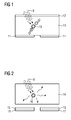
- the FIG. 1 shows an X-ray detector for direct X-ray conversion according to the known prior art.
- a material 13 suitable for absorption and direct conversion of X-ray X is disposed between a pixel electrode 11 and a top electrode 12.
- the pixelation of the electrode 11 is made for spatial resolution.
- the top electrode 12 is transparent to X-rays X.
- the X-ray X is absorbed in the material 13 to form electron-hole pairs.
- the conversion center 16 is shown, in which the conversion of the radiation energy of the X-ray X into electrical energy takes place, in which the energy of the radiation passes to an electron and this in a higher energetic Condition is lifted.
- the electron-hole pair thus formed can be separated in an applied field which can be applied to the material layer 13 via the electrodes 11, 12. That is, the X-ray detector is in operation under a bias voltage and upon absorption of X-radiation X, a current flow I can be detected.
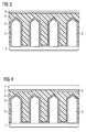
- FIG. 2 shows an X-ray detector for indirect X-ray conversion according to the prior art.
- This X-ray detector for indirect X-ray conversion is constructed in two parts.
- the X-ray detector comprises a scintillation layer 14 in which the conversion of X-radiation X into fluorescence radiation takes place.
- a conversion center 16 is shown schematically, in which the conversion of the energy of the X-ray radiation into light energy passes.
- the second part of the X-ray detector comprises photodetectors 15, in particular photodiodes 15, and in turn pixelated electrodes 11. These photodiodes 15 are suitable for detecting the fluorescence radiation of the scintillator layer 14.
- Known scintillator materials which can be used for a scintillator layer are e.g. Gadolinium sulfur oxide or cesium iodide.
- the layer thickness of such a scintillation layer is 0.1 mm to 1 mm.
- the direct X-ray conversion layer 13 may be a silicon photodiode having a high layer thickness of more than 1 cm, or amorphous selenium may be used as a direct X-ray converter.
- the selenium layers for direct x-ray conversion are usually up to 1 mm thick.
- the direct x-ray converters are used e.g. biased in the reverse direction with voltages in the range of a few kV.
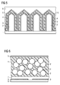
- FIGS. 3, 4 and 5 each show an X-ray detector with a hybrid photoactive layer, wherein the scintillators 2 scintillator needles, which are grown on a substrate 1.
- the scintillator needles 2 are, for example, cesium iodide scintillators.
- the substrate 1 may be a glass substrate be.
- An ALD layer 3 is deposited over the scintillator needles 2 grown on the glass substrate 1.
- the ALD layer 3 is a transparent conductive oxide (TCO). This ALD layer 3 can thus fulfill the function of the anode of the hybrid photodiode.
- TCO transparent conductive oxide
- the interstices of the scintillator needles 2 on the substrate 1 are filled with a bulk heterojunction 4 and the needles 2 are covered therewith, so that a thick hybrid photoactive layer is formed in which the scintillator needles 2 are completely embedded.
- the hybrid photoactive layer is covered by a cathode 5.
- This can in turn be applied by an ALD process.
- aluminum is used for this purpose.
- the cathode 5 can also be made by thermal evaporation of one or more metals. In FIG. 3 the cathode 5 is applied over a large area to the photoactive layer.
- the application of the anode 3 by an ALD process to the scintillator needles 2 has the advantage that an isotropic deposition takes place even with a high aspect ratio of the scintillator needle 2.
- FIG. 4 Also shown is a substrate 1 with raised scintillator needles 2 covered by an ALD layer 3. Again, the deposition of a bulk heterojunction 4 occurs in the needle interstices and on the scintillator needles 2 so that they are completely embedded in the bulk heterojunction 4 and form a hybrid photoactive layer with the bulk heterojunction 4.
- the top electrode 5, which represents the cathode of the hybrid photodiode, is shown pixelated in this case, ie, the cathode 5 is interrupted and it can thus be a spatial resolution. Above the cathode 5, a further substrate 1 is shown. This can be part of an encapsulation of the X-ray detector.
- the hybrid photoactive layer may be completely encapsulated to protect it against the ingress of moisture which could adversely affect the organic materials and also adversely affect hygroscopic scintillator material.
- FIG. 5 shows an alternative embodiment of the X-ray detector in which the scintillator needles 2 are grown back on a substrate 1 and both electrodes 3, 5 were deposited isotropically by ALD process.
- the anode 3 is deposited directly on the scintillator needles 2.
- the cathode 5 is deposited on the bulk heterojunction 4.
- the bulk heterojunction 4 is deposited in this case only as a relatively thin layer over the needles 2. In particular, the bulk heterojunction 4 is less than 100 nm in layer thickness.
- the electrode layers 3,5 and the bulk heterojunction 4 thus still form the needle structure.
- the interspinous spaces are then filled with a filling material 6 and the scintillator tips covered with it.
- filler 6 for example, an epoxide can be used. This serves primarily for stabilization and moisture protection of the hybrid photodetector.
- the anode 3 is always arranged between the scintillators 2 and the bulk heterojunction 4.
- the scintillation radiation In order for the scintillation radiation, which is excited in the scintillators 2 by the penetrating X-ray radiation X, to be absorbed by the bulk heterojunction 4, the scintillation radiation must be able to exit through the anode 3 into the bulk heterojunction 4.
- a transparent conductive oxide (TCO) is used as the anode 3. This can be deposited in particular by an ALD process. The transparency must be ensured, above all, in the wavelength range in which the scintillators 2 emit radiation. In this case, an isotropic emission can take place in the photoactive organic semiconductor material 4.
- the X-ray detector can be used for dose rate measurement.
- pixelated electrodes 3, 5 are used, in this case preferably a pixelated cathode 5, as in FIG. 4 shown.
- Particularly advantageous for this purpose is an ALD-deposited anode 3 which has a refractive index which causes the scintillation radiation to be totally reflected at the surface of the scintillators 2 and conducted in the scintillator needles 2 as in an optical waveguide. Then, if an interruption of the ALD layer, preferably provided at the needle tips, the fluorescence radiation occurs bundled at this point and ensures a high spatial resolution of the X-ray detector.
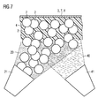
- the FIG. 6 1 shows a hybrid photodiode with embedded scintillator particles 2 in the bulk heterojunction 4.
- This hybrid photoactive layer is arranged between a cathode 5 and a substrate 8 with pixelated anodes 3. Between the pixelated anodes 3 and the hybrid photoactive layer may still be an intermediate layer 7. In general, intermediate layers 7 or so-called interlayer 7 can be used to promote charge transport to the electrodes 3, 5.
- the substrate 8 is in this case an active matrix backplane, via which the pixel anodes 3 can be controlled and read out.
- the conversion of X-radiation X into fluorescence radiation takes place in the scintillators 2.
- the fluorescence radiation is absorbed in the bulk heterojunction 4 and converted into electrical energy.
- the electron-hole pairs generated by the absorption of the fluorescence radiation are as well as in FIG. 1 shown separated in the applied field between anode 3 and cathode 5 and detected.
- an isotropic emission of the fluorescence radiation into the bulk heterojunction 4 takes place. This causes an efficient conversion of the X-ray energy into electrical signals.
- the layer thickness of the hybrid photoactive layer with the bulk heterojunction 4 and the embedded scintillators 2 is about 100 microns, but may also be only 10 microns, depending on the application. For example, very thin layer thicknesses of the hybrid photoactive layer of about 1 ⁇ m are possible.
- the structuring of the electrodes 3, 5 determines the active area of the hybrid photodiodes.
- the pixelation of the electrodes 3, 5, depending on whether on the substrate 1, 8 or on the bulk heterojunction 4, can preferably take place via shadow masks or lithographically.
- the structuring by shadow masks is advantageous in a direct Aufdampfvorgang the top electrode.
- the pixel pitch is preferably 50 ⁇ m.
- the active diode area is chosen to be very large, especially for dose rate measurements, and can be up to 10 cm 2 .
- FIG. 7 now shows schematically the manufacturing process of a hybrid photodetector with particulate scintillators 2.
- the hybrid photoactive layer is applied in a co-spraying. That is, the bulk heterojunction (BHJ) 4 is sprayed from a solution 40 simultaneously with a suspension 20 containing the scintillator particles 2.
- BHJ bulk heterojunction
- two spray heads 21, 41 are shown, which are aligned on the same substrate 3, 7, 8.
- the layer thickness of the hybrid photoactive layer can be adjusted in a targeted manner.
- the sprayed layer thicknesses are between 0.5 and 100 microns.
- Advantageous proportions of scintillator particles 2 in the bulk heterojunction 4 are between 10% by volume and 50% by volume.
- the scintillator is discretely applied to the substrate in this co-spraying process.
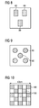
- FIGS. 8, 9 and 10 show sensors with a dimension of 43 x 43 cm, as they can be used in existing X-ray equipment for dose rate measurement of the so-called Automatic Exposure Control (AEC).
- AEC Automatic Exposure Control
- the three-field arrangement, as in FIG. 8 shown covers the lung and mediastinal area, as it is important in medical applications of x-ray equipment.
- the hatched areas 80, 90 in the FIGS. 8 and 9 represent the sensor surfaces.
- an inventive arrangement of sensor surfaces 100 is shown, as they can be particularly well realized by the X-ray detectors according to the invention with hybrid photoactive layer. These are very thin and can be separated over a large area.
- a kind of checkerboard pattern that is, an arrangement of the sensors 100 in a two-dimensional 5x5 matrix done.
- a sensor with several, eg 13 sensor fields 100, it is possible to react very flexibly to objects to be examined differently.
- Various combinations of the sensor fields 100 can be actively switched and used.
- the sensor fields 100 for dose rate measurement must not cast shadows on the X-ray image.
- the FIG. 11 shows an X-ray device 70 as used for the examination of an examination subject 700, for example in medicine.
- the examination object 700 is attached above the x-ray detector unit 73, 74.
- This consists of an X-ray detector for dose rate measurement 73 and an X-ray detector for the imaging 74.
- an X-ray detector for dose rate measurement can also be attached above the examination subject 700.
- the X-ray tube 72 in which the X-ray X is generated, is arranged so that the X-ray X penetrates the examination subject 700 and then hits the X-ray detector unit 73, 74.
- a driver 71 of the X-ray tube 72 is shown.
- This image of an X-ray machine shows that two X-ray detectors 73, 74 with very different requirements for the X-ray measurement are necessary.
- it has hitherto been necessary to apply very different technologies for X-ray imaging e.g. via indirect converters and for X-ray dose rate measurement e.g. recourse to ionization chambers.
- an X-ray detector for dose rate measurement as well as for imaging can be produced.
- the dose rate measurement it is advantageous for the dose rate measurement to have a low component depth in order to absorb as little X-radiation as possible, since this is still intended to impinge on the imaging in the second X-ray detector 74 for imaging.
- the efficient conversion of the energy of the X-radiation X into signal charges is of particular importance.
- the highest possible radiation should be absorbed. It is always about a trade-off between absorption and actual performance. That the quantum efficiency and the dynamic behavior of the X-ray diode deteriorate with increasing layer thickness.
- the absorption of the X-ray X in the hybrid photoactive layer increases exponentially with the layer thickness.
- the absorption should be low.
- layer thicknesses between 5 and 20 microns and a Szintillatoranteil of 50 vol .-% of advantage For X-ray imaging, layer thicknesses between 100 ⁇ m and 1 mm are preferably used.
- scintillator needles 2 with an ALD layer jacket 3 are advantageous, by which the scintillator needles 2 function as optical waveguides.
- the FIG. 12 shows a diagram in which the efficiency of the conversion of the different X-ray detectors is shown.
- the measurement results A and C are each assigned to an X-ray detector based on indirect conversion, the measurement results B an X-ray detector based on direct conversion.
- the measured current I n which was normalized to the dose rate and to the layer thickness of the respective X-ray detector.
- the current is indicated in amperes.
- the dose rate in micro-gray per second ( ⁇ Gr / s).
- an organic X-ray detector based on a bulk heterojunction with embedded lead-selenium quantum dots was used as an X-ray detector based on direct conversion. Its measurement results are marked B in the diagram.
- the quantum dots account for 50% by volume of the conversion layer.
- the embedding of quantum dots, so-called quantum dots, in an organic semiconductor material is based on direct X-ray conversion in the quantum dots, wherein the organic semiconductor material is responsible for the removal of the generated electrical charge.
- the measurement points labeled A are a prior art two-piece x-ray detector as in FIG FIG. 2 shown, assign. In this case, organic photodiodes were used as the photodetector and a 1 mm thick cesium iodide scintillator.
- the measurement designated C is assigned to a hybrid X-ray detector according to the invention comprising a hybrid photoactive layer of a bulk heterojunction 4 and embedded scintillator particles 2 of gadolinium sulfur oxide. These were deposited by the co-spraying process according to the invention.
- the hybrid photoactive layer is 10 ⁇ m.
- the gadolinium sulfur oxide particles account for 50% by volume of the active layer.
- the conversion efficiency can be tuned over the layer thickness.
- the evaluation of the various X-ray detectors takes place at a known dose rate ( ⁇ G / s).
- a difference between the embedded quantum dots and the scintillator particles 2 is in the size of the particles.
- the scintillator particles 2 are between 1 .mu.m and 4 .mu.m in diameter.
- the quantum dots range in diameter between 3 nm and 6 nm. Therefore, the conversion principle differs.
- the X-rays are converted directly into electrical charge and the organic Semiconductor material serves as a carrier for the quantum dots and as a conductive material for the removal of the charge.
- the scintillator particles the X-radiation is converted into scintillating radiation, which lies in particular in visible light, and is converted into charge via an organic photoactive material.
Landscapes
- Physics & Mathematics (AREA)
- Health & Medical Sciences (AREA)
- Life Sciences & Earth Sciences (AREA)
- General Physics & Mathematics (AREA)
- High Energy & Nuclear Physics (AREA)
- Molecular Biology (AREA)
- Spectroscopy & Molecular Physics (AREA)
- Chemical & Material Sciences (AREA)
- Crystallography & Structural Chemistry (AREA)
- Measurement Of Radiation (AREA)
- Light Receiving Elements (AREA)
Applications Claiming Priority (1)
| Application Number | Priority Date | Filing Date | Title |
|---|---|---|---|
| DE102010043749A DE102010043749A1 (de) | 2010-11-11 | 2010-11-11 | Hybride organische Fotodiode |
Publications (3)
| Publication Number | Publication Date |
|---|---|
| EP2453263A2 true EP2453263A2 (fr) | 2012-05-16 |
| EP2453263A3 EP2453263A3 (fr) | 2012-06-27 |
| EP2453263B1 EP2453263B1 (fr) | 2015-10-14 |
Family
ID=45002923
Family Applications (1)
| Application Number | Title | Priority Date | Filing Date |
|---|---|---|---|
| EP11185221.6A Not-in-force EP2453263B1 (fr) | 2010-11-11 | 2011-10-14 | Photodiode organique hybride |
Country Status (6)
| Country | Link |
|---|---|
| US (1) | US8637831B2 (fr) |
| EP (1) | EP2453263B1 (fr) |
| KR (1) | KR101844392B1 (fr) |
| CN (1) | CN102468441B (fr) |
| DE (1) | DE102010043749A1 (fr) |
| WO (1) | WO2012062625A2 (fr) |
Cited By (5)
| Publication number | Priority date | Publication date | Assignee | Title |
|---|---|---|---|---|
| NL2011593C2 (en) * | 2013-10-11 | 2015-04-14 | Argus Imaging | Scintillator. |
| WO2015091067A1 (fr) * | 2013-12-18 | 2015-06-25 | Siemens Aktiengesellschaft | Détecteur de rayons x organique hybride comportant des canaux conducteurs |
| EP2739701B1 (fr) | 2011-08-02 | 2016-02-10 | Vieworks Co. Ltd. | Nouvelle composition pour un détecteur d'imagerie par rayonnement et détecteur d'imagerie par rayonnement qui comprend cette dernière |
| WO2016153335A1 (fr) | 2015-03-20 | 2016-09-29 | Perkinelmer Health Sciences B.V. | Scintillateur |
| CN115144888A (zh) * | 2021-03-30 | 2022-10-04 | 西门子医疗有限公司 | 具有无死区的对接的吸收体拼块的辐射检测器 |
Families Citing this family (32)
| Publication number | Priority date | Publication date | Assignee | Title |
|---|---|---|---|---|
| US9425234B2 (en) | 2010-07-15 | 2016-08-23 | Leigh E. Colby | Quantum dot digital radiographic detection system |
| US9935152B2 (en) | 2012-12-27 | 2018-04-03 | General Electric Company | X-ray detector having improved noise performance |
| DE102013200881A1 (de) | 2013-01-21 | 2014-07-24 | Siemens Aktiengesellschaft | Nanopartikulärer Szintillatoren und Verfahren zur Herstellung nanopartikulärer Szintillatoren |
| RU2532645C1 (ru) * | 2013-04-29 | 2014-11-10 | Общество с ограниченной ответственностью "Научно-технический центр "МТ" (ООО "НТЦ-МТ") | Способ формирования структурированного сцинтиллятора на поверхности пикселированного фотоприемника (варианты) и сцинтилляционный детектор, полученнный данным способом (варианты) |
| US9362341B2 (en) | 2013-12-09 | 2016-06-07 | General Electric Company | X ray detection apparatus |
| US9917133B2 (en) | 2013-12-12 | 2018-03-13 | General Electric Company | Optoelectronic device with flexible substrate |
| DE102014203685A1 (de) * | 2014-02-28 | 2015-09-03 | Siemens Aktiengesellschaft | Konversionsfolie zur Konversion von ionisierender Strahlung, Strahlungsdetektor und Verfahren zu Herstellung |
| DE102014212424A1 (de) | 2013-12-18 | 2015-06-18 | Siemens Aktiengesellschaft | Szintillatoren mit organischer Photodetektions-Schale |
| US10732131B2 (en) | 2014-03-13 | 2020-08-04 | General Electric Company | Curved digital X-ray detector for weld inspection |
| TW201543061A (zh) * | 2014-05-13 | 2015-11-16 | Architek Material Co Ltd | 閃光體面板、輻射顯像裝置及其製作方法 |
| US9753148B2 (en) * | 2014-05-22 | 2017-09-05 | Saint-Gobain Ceramics & Plastics, Inc. | Radiation sensor and methods of detecting a targeted radiation using the radiation sensor |
| DE102014225543B4 (de) | 2014-12-11 | 2021-02-25 | Siemens Healthcare Gmbh | Perowskit-Partikel mit Beschichtung aus einem Halbleitermaterial, Verfahren zu deren Herstellung, Detektor, umfassend beschichtete Partikel, Verfahren zur Herstellung eines Detektors und Verfahren zur Herstellung einer Schicht umfassend beschichtete Partikel |
| US9941433B2 (en) * | 2014-12-11 | 2018-04-10 | Vadient Optics, Llc | Composite quantum-dot materials for photonic detectors |
| DE102014225541A1 (de) | 2014-12-11 | 2016-06-16 | Siemens Healthcare Gmbh | Detektionsschicht umfassend Perowskitkristalle |
| DE102015006839A1 (de) * | 2015-06-02 | 2016-12-08 | Karlsruher Institut für Technologie | Optoelektronische Struktur zur Detektion von elektromagnetischer Strahlung |
| DE102015220793A1 (de) | 2015-10-23 | 2017-04-27 | Siemens Healthcare Gmbh | Röntgendetektor und/oder Gammadetektor mit Lichtbias |
| US10571580B2 (en) | 2015-11-11 | 2020-02-25 | Siemens Healthcare Gmbh | Detector element for detecting incident x-ray radiation |
| US9841509B2 (en) | 2015-11-24 | 2017-12-12 | General Electric Company | Processes for fabricating organic x-ray detectors, related x-ray detectors and systems |
| US9929216B2 (en) | 2015-11-24 | 2018-03-27 | General Electric Company | Processes for fabricating organic X-ray detectors, related organic X-ray detectors and systems |
| DE102015225134A1 (de) | 2015-12-14 | 2017-06-14 | Siemens Healthcare Gmbh | Hybride Röntgendetektoren realisiert mittels Soft-sintern von zwei oder mehreren durchmischten Pulvern |
| WO2017163149A1 (fr) * | 2016-03-23 | 2017-09-28 | Koninklijke Philips N.V. | Détecteur d'imagerie de nanomatériau avec bordure de pixel intégrée |
| US10641912B1 (en) | 2016-06-15 | 2020-05-05 | Triad National Security, Llc | “4H” X-ray camera |
| JP6735215B2 (ja) * | 2016-11-21 | 2020-08-05 | 株式会社東芝 | 放射線検出器 |
| JP2018157054A (ja) * | 2017-03-17 | 2018-10-04 | 株式会社東芝 | 光検出素子、および光検出器 |
| US10797110B2 (en) | 2017-07-10 | 2020-10-06 | General Electric Company | Organic photodiode pixel for image detectors |
| US10267931B1 (en) * | 2018-02-06 | 2019-04-23 | Siemens Medical Solutions Usa, Inc. | Radiation detector capable of measuring depth-of-interaction |
| CN109244096B (zh) * | 2018-09-20 | 2020-07-24 | 深圳先进技术研究院 | X射线平板探测器及其制作方法 |
| EP3629064A1 (fr) | 2018-09-25 | 2020-04-01 | Koninklijke Philips N.V. | Réseau de scintillateurs à haute efficacité quantique de détection |
| KR102634270B1 (ko) * | 2018-11-27 | 2024-02-06 | 한국전기연구원 | 저선량 및 고해상도 구강 방사선 디텍터 |
| CN111883550B (zh) * | 2020-08-10 | 2022-07-01 | 上海大学 | 一种平板探测器 |
| GB2607713B (en) * | 2021-05-26 | 2023-09-20 | Thermo Fisher Scient Bremen Gmbh | Systems and methods for imaging and ablating a sample |
| CN119421513B (zh) * | 2024-09-23 | 2025-12-16 | 浙江大学 | 一种基于液体介质光致极化的自驱动异质结构x射线探测器及其制备方法 |
Family Cites Families (10)
| Publication number | Priority date | Publication date | Assignee | Title |
|---|---|---|---|---|
| US5116559A (en) * | 1991-02-26 | 1992-05-26 | General Electric Company | Method of forming yttria-gadolinia ceramic scintillator using hydroxide coprecipitation step |
| TW410478B (en) * | 1998-05-29 | 2000-11-01 | Lucent Technologies Inc | Thin-film transistor monolithically integrated with an organic light-emitting diode |
| DE10313602B4 (de) | 2003-03-26 | 2013-05-08 | Siemens Aktiengesellschaft | Vorrichtung zur Messung einer Strahlungsdosis |
| US7151006B2 (en) * | 2003-11-04 | 2006-12-19 | Varian Medical Systems Technologies, Inc. | Process to reduce the dark current in semiconducting films |
| US20070272872A1 (en) * | 2006-05-24 | 2007-11-29 | Bruker Axs, Inc. | X-ray detector with photodetector embedded in scintillator |
| DE102006039785A1 (de) * | 2006-08-24 | 2008-02-28 | Siemens Ag | Photodetektor sowie Verwendung des Photodetektors in einem Röntgenkontrollsystem |
| US20100163737A1 (en) * | 2007-05-24 | 2010-07-01 | Satoshi Masuda | Radiation detector, method of manufacturing radiation detector, and method of manufacturing supporting substrate |
| DE102008029782A1 (de) * | 2008-06-25 | 2012-03-01 | Siemens Aktiengesellschaft | Photodetektor und Verfahren zur Herstellung dazu |
| US20100074396A1 (en) * | 2008-07-07 | 2010-03-25 | Siemens Medical Solutions Usa, Inc. | Medical imaging with black silicon photodetector |
| CN101660115B (zh) * | 2009-09-18 | 2011-08-31 | 武汉理工大学 | 纳米氧化锆热障涂层的制备方法 |
-
2010
- 2010-11-11 DE DE102010043749A patent/DE102010043749A1/de not_active Withdrawn
-
2011
- 2011-10-14 EP EP11185221.6A patent/EP2453263B1/fr not_active Not-in-force
- 2011-11-02 KR KR1020137012202A patent/KR101844392B1/ko not_active Expired - Fee Related
- 2011-11-02 WO PCT/EP2011/069203 patent/WO2012062625A2/fr not_active Ceased
- 2011-11-11 CN CN201110356837.6A patent/CN102468441B/zh not_active Expired - Fee Related
- 2011-11-11 US US13/294,385 patent/US8637831B2/en not_active Expired - Fee Related
Non-Patent Citations (1)
| Title |
|---|
| None |
Cited By (8)
| Publication number | Priority date | Publication date | Assignee | Title |
|---|---|---|---|---|
| EP2739701B1 (fr) | 2011-08-02 | 2016-02-10 | Vieworks Co. Ltd. | Nouvelle composition pour un détecteur d'imagerie par rayonnement et détecteur d'imagerie par rayonnement qui comprend cette dernière |
| NL2011593C2 (en) * | 2013-10-11 | 2015-04-14 | Argus Imaging | Scintillator. |
| WO2015091067A1 (fr) * | 2013-12-18 | 2015-06-25 | Siemens Aktiengesellschaft | Détecteur de rayons x organique hybride comportant des canaux conducteurs |
| US9869773B2 (en) | 2013-12-18 | 2018-01-16 | Siemens Aktiengesellschaft | Hybrid-organic X-ray detector with conductive channels |
| WO2016153335A1 (fr) | 2015-03-20 | 2016-09-29 | Perkinelmer Health Sciences B.V. | Scintillateur |
| US10670741B2 (en) | 2015-03-20 | 2020-06-02 | Varex Imaging Corporation | Scintillator |
| CN115144888A (zh) * | 2021-03-30 | 2022-10-04 | 西门子医疗有限公司 | 具有无死区的对接的吸收体拼块的辐射检测器 |
| US12433044B2 (en) | 2021-03-30 | 2025-09-30 | Siemens Healthineers Ag | Apparatuses for radiation detection including absorber tiles with a semiconductor material or a perovskite material disposed between the absorber tiles and methods of manufacturing the same |
Also Published As
| Publication number | Publication date |
|---|---|
| KR101844392B1 (ko) | 2018-04-03 |
| DE102010043749A1 (de) | 2012-05-16 |
| WO2012062625A3 (fr) | 2012-07-26 |
| WO2012062625A2 (fr) | 2012-05-18 |
| KR20130142130A (ko) | 2013-12-27 |
| US20120121067A1 (en) | 2012-05-17 |
| EP2453263B1 (fr) | 2015-10-14 |
| US8637831B2 (en) | 2014-01-28 |
| EP2453263A3 (fr) | 2012-06-27 |
| CN102468441B (zh) | 2016-04-13 |
| CN102468441A (zh) | 2012-05-23 |
Similar Documents
| Publication | Publication Date | Title |
|---|---|---|
| EP2453263B1 (fr) | Photodiode organique hybride | |
| DE10244176A1 (de) | Bilddetektor für Röntgenstrahlung | |
| DE69514495T2 (de) | Festkörper-bildverstärker und röntgenuntersuchungsgerät mit einem festkörper-bildverstärker | |
| EP3362820B1 (fr) | Élément détecteur destiné à la détection de rayons x incidents | |
| EP3066495B1 (fr) | Détecteur hybrid organique de rayons x avec canaux conducteurs | |
| EP2251713A1 (fr) | Détecteur de vérification du rayonnement ionisant | |
| DE10313602B4 (de) | Vorrichtung zur Messung einer Strahlungsdosis | |
| WO2015091196A1 (fr) | Scintillateurs pourvus d'une enveloppe de photodétection organique | |
| DE112005002398T5 (de) | Hochauflösender Halbleiterkristall-Bildgeber | |
| DE102014225541A1 (de) | Detektionsschicht umfassend Perowskitkristalle | |
| DE102016205818A1 (de) | Vorrichtung und Verfahren zum Detektieren von Röntgenstrahlung | |
| DE102012215818A1 (de) | Strahlungsdetektor und Verfahren zur Herstellung eines Strahlungsdetektors | |
| WO2010119019A1 (fr) | Dispositif de détection et appareil de tomographie à rayons x pour effectuer des mesures de contraste de phase et procédé pour effectuer une mesure de contraste de phase | |
| DE102015220793A1 (de) | Röntgendetektor und/oder Gammadetektor mit Lichtbias | |
| WO2015091145A1 (fr) | Film de conversion pour convertir un rayonnement ionisant, détecteur de rayonnement et procédé de fabrication | |
| DE102006029104A1 (de) | Verfahren und Vorrichtung zur Reduktion der Polarisierung in einer bildgebenden Einrichtung | |
| DE10318416B4 (de) | Vorrichtung zur Erfassung des Abstandes und der Richtung einer Röntgenstrahl- oder Gammastrahlquelle mit einem Mehrschichtstrahlendetektor | |
| WO2014019817A2 (fr) | Détecteur de rayons x, système de ct et procédés associés | |
| DE102012202200B3 (de) | Röntgenstrahlungsdetektor und Verfahren zum Messen von Röntgenstrahlung | |
| DE102011077961A1 (de) | Schwachlichtdetektion mit organischem fotosensitivem Bauteil | |
| DE102011085080A1 (de) | Verfahren und Vorrichtung zur Detektion von Röntgenquanten | |
| DE102012213411B4 (de) | Verfahren zur Detektion von Röntgenstrahlung | |
| DE102015225134A1 (de) | Hybride Röntgendetektoren realisiert mittels Soft-sintern von zwei oder mehreren durchmischten Pulvern | |
| DE102014203685A1 (de) | Konversionsfolie zur Konversion von ionisierender Strahlung, Strahlungsdetektor und Verfahren zu Herstellung | |
| DE102011080892B3 (de) | Röntgenstrahlungsdetektor zur Verwendung in einem CT-System |
Legal Events
| Date | Code | Title | Description |
|---|---|---|---|
| PUAI | Public reference made under article 153(3) epc to a published international application that has entered the european phase |
Free format text: ORIGINAL CODE: 0009012 |
|
| AK | Designated contracting states |
Kind code of ref document: A2 Designated state(s): AL AT BE BG CH CY CZ DE DK EE ES FI FR GB GR HR HU IE IS IT LI LT LU LV MC MK MT NL NO PL PT RO RS SE SI SK SM TR |
|
| AX | Request for extension of the european patent |
Extension state: BA ME |
|
| REG | Reference to a national code |
Ref country code: DE Ref legal event code: R079 Ref document number: 502011008085 Country of ref document: DE Free format text: PREVIOUS MAIN CLASS: G01T0001020000 Ipc: G01T0001200000 |
|
| PUAL | Search report despatched |
Free format text: ORIGINAL CODE: 0009013 |
|
| AK | Designated contracting states |
Kind code of ref document: A3 Designated state(s): AL AT BE BG CH CY CZ DE DK EE ES FI FR GB GR HR HU IE IS IT LI LT LU LV MC MK MT NL NO PL PT RO RS SE SI SK SM TR |
|
| AX | Request for extension of the european patent |
Extension state: BA ME |
|
| RIC1 | Information provided on ipc code assigned before grant |
Ipc: G01T 1/20 20060101AFI20120521BHEP Ipc: G01T 1/02 20060101ALI20120521BHEP |
|
| 17P | Request for examination filed |
Effective date: 20120906 |
|
| RAP1 | Party data changed (applicant data changed or rights of an application transferred) |
Owner name: SIEMENS AKTIENGESELLSCHAFT |
|
| 17Q | First examination report despatched |
Effective date: 20140411 |
|
| GRAP | Despatch of communication of intention to grant a patent |
Free format text: ORIGINAL CODE: EPIDOSNIGR1 |
|
| INTG | Intention to grant announced |
Effective date: 20150511 |
|
| GRAS | Grant fee paid |
Free format text: ORIGINAL CODE: EPIDOSNIGR3 |
|
| GRAA | (expected) grant |
Free format text: ORIGINAL CODE: 0009210 |
|
| AK | Designated contracting states |
Kind code of ref document: B1 Designated state(s): AL AT BE BG CH CY CZ DE DK EE ES FI FR GB GR HR HU IE IS IT LI LT LU LV MC MK MT NL NO PL PT RO RS SE SI SK SM TR |
|
| REG | Reference to a national code |
Ref country code: GB Ref legal event code: FG4D Free format text: NOT ENGLISH |
|
| REG | Reference to a national code |
Ref country code: AT Ref legal event code: REF Ref document number: 755558 Country of ref document: AT Kind code of ref document: T Effective date: 20151015 Ref country code: CH Ref legal event code: EP |
|
| REG | Reference to a national code |
Ref country code: FR Ref legal event code: PLFP Year of fee payment: 5 |
|
| REG | Reference to a national code |
Ref country code: IE Ref legal event code: FG4D Free format text: LANGUAGE OF EP DOCUMENT: GERMAN |
|
| REG | Reference to a national code |
Ref country code: DE Ref legal event code: R096 Ref document number: 502011008085 Country of ref document: DE |
|
| REG | Reference to a national code |
Ref country code: NL Ref legal event code: MP Effective date: 20151014 |
|
| REG | Reference to a national code |
Ref country code: LT Ref legal event code: MG4D |
|
| PG25 | Lapsed in a contracting state [announced via postgrant information from national office to epo] |
Ref country code: IT Free format text: LAPSE BECAUSE OF FAILURE TO SUBMIT A TRANSLATION OF THE DESCRIPTION OR TO PAY THE FEE WITHIN THE PRESCRIBED TIME-LIMIT Effective date: 20151014 Ref country code: IS Free format text: LAPSE BECAUSE OF FAILURE TO SUBMIT A TRANSLATION OF THE DESCRIPTION OR TO PAY THE FEE WITHIN THE PRESCRIBED TIME-LIMIT Effective date: 20160214 Ref country code: HR Free format text: LAPSE BECAUSE OF FAILURE TO SUBMIT A TRANSLATION OF THE DESCRIPTION OR TO PAY THE FEE WITHIN THE PRESCRIBED TIME-LIMIT Effective date: 20151014 Ref country code: ES Free format text: LAPSE BECAUSE OF FAILURE TO SUBMIT A TRANSLATION OF THE DESCRIPTION OR TO PAY THE FEE WITHIN THE PRESCRIBED TIME-LIMIT Effective date: 20151014 Ref country code: NO Free format text: LAPSE BECAUSE OF FAILURE TO SUBMIT A TRANSLATION OF THE DESCRIPTION OR TO PAY THE FEE WITHIN THE PRESCRIBED TIME-LIMIT Effective date: 20160114 Ref country code: LT Free format text: LAPSE BECAUSE OF FAILURE TO SUBMIT A TRANSLATION OF THE DESCRIPTION OR TO PAY THE FEE WITHIN THE PRESCRIBED TIME-LIMIT Effective date: 20151014 Ref country code: NL Free format text: LAPSE BECAUSE OF FAILURE TO SUBMIT A TRANSLATION OF THE DESCRIPTION OR TO PAY THE FEE WITHIN THE PRESCRIBED TIME-LIMIT Effective date: 20151014 |
|
| PG25 | Lapsed in a contracting state [announced via postgrant information from national office to epo] |
Ref country code: LV Free format text: LAPSE BECAUSE OF FAILURE TO SUBMIT A TRANSLATION OF THE DESCRIPTION OR TO PAY THE FEE WITHIN THE PRESCRIBED TIME-LIMIT Effective date: 20151014 Ref country code: GR Free format text: LAPSE BECAUSE OF FAILURE TO SUBMIT A TRANSLATION OF THE DESCRIPTION OR TO PAY THE FEE WITHIN THE PRESCRIBED TIME-LIMIT Effective date: 20160115 Ref country code: FI Free format text: LAPSE BECAUSE OF FAILURE TO SUBMIT A TRANSLATION OF THE DESCRIPTION OR TO PAY THE FEE WITHIN THE PRESCRIBED TIME-LIMIT Effective date: 20151014 Ref country code: PL Free format text: LAPSE BECAUSE OF FAILURE TO SUBMIT A TRANSLATION OF THE DESCRIPTION OR TO PAY THE FEE WITHIN THE PRESCRIBED TIME-LIMIT Effective date: 20151014 Ref country code: PT Free format text: LAPSE BECAUSE OF FAILURE TO SUBMIT A TRANSLATION OF THE DESCRIPTION OR TO PAY THE FEE WITHIN THE PRESCRIBED TIME-LIMIT Effective date: 20160215 Ref country code: RS Free format text: LAPSE BECAUSE OF FAILURE TO SUBMIT A TRANSLATION OF THE DESCRIPTION OR TO PAY THE FEE WITHIN THE PRESCRIBED TIME-LIMIT Effective date: 20151014 Ref country code: SE Free format text: LAPSE BECAUSE OF FAILURE TO SUBMIT A TRANSLATION OF THE DESCRIPTION OR TO PAY THE FEE WITHIN THE PRESCRIBED TIME-LIMIT Effective date: 20151014 |
|
| REG | Reference to a national code |
Ref country code: CH Ref legal event code: PL |
|
| RAP2 | Party data changed (patent owner data changed or rights of a patent transferred) |
Owner name: SIEMENS HEALTHCARE GMBH |
|
| REG | Reference to a national code |
Ref country code: DE Ref legal event code: R097 Ref document number: 502011008085 Country of ref document: DE |
|
| REG | Reference to a national code |
Ref country code: IE Ref legal event code: MM4A |
|
| PG25 | Lapsed in a contracting state [announced via postgrant information from national office to epo] |
Ref country code: CZ Free format text: LAPSE BECAUSE OF FAILURE TO SUBMIT A TRANSLATION OF THE DESCRIPTION OR TO PAY THE FEE WITHIN THE PRESCRIBED TIME-LIMIT Effective date: 20151014 Ref country code: CH Free format text: LAPSE BECAUSE OF NON-PAYMENT OF DUE FEES Effective date: 20151031 Ref country code: LI Free format text: LAPSE BECAUSE OF NON-PAYMENT OF DUE FEES Effective date: 20151031 |
|
| PLBE | No opposition filed within time limit |
Free format text: ORIGINAL CODE: 0009261 |
|
| REG | Reference to a national code |
Ref country code: DE Ref legal event code: R081 Ref document number: 502011008085 Country of ref document: DE Owner name: SIEMENS HEALTHCARE GMBH, DE Free format text: FORMER OWNER: SIEMENS AKTIENGESELLSCHAFT, 80333 MUENCHEN, DE |
|
| STAA | Information on the status of an ep patent application or granted ep patent |
Free format text: STATUS: NO OPPOSITION FILED WITHIN TIME LIMIT |
|
| PG25 | Lapsed in a contracting state [announced via postgrant information from national office to epo] |
Ref country code: DK Free format text: LAPSE BECAUSE OF FAILURE TO SUBMIT A TRANSLATION OF THE DESCRIPTION OR TO PAY THE FEE WITHIN THE PRESCRIBED TIME-LIMIT Effective date: 20151014 Ref country code: SK Free format text: LAPSE BECAUSE OF FAILURE TO SUBMIT A TRANSLATION OF THE DESCRIPTION OR TO PAY THE FEE WITHIN THE PRESCRIBED TIME-LIMIT Effective date: 20151014 Ref country code: EE Free format text: LAPSE BECAUSE OF FAILURE TO SUBMIT A TRANSLATION OF THE DESCRIPTION OR TO PAY THE FEE WITHIN THE PRESCRIBED TIME-LIMIT Effective date: 20151014 Ref country code: RO Free format text: LAPSE BECAUSE OF FAILURE TO SUBMIT A TRANSLATION OF THE DESCRIPTION OR TO PAY THE FEE WITHIN THE PRESCRIBED TIME-LIMIT Effective date: 20151014 Ref country code: SM Free format text: LAPSE BECAUSE OF FAILURE TO SUBMIT A TRANSLATION OF THE DESCRIPTION OR TO PAY THE FEE WITHIN THE PRESCRIBED TIME-LIMIT Effective date: 20151014 |
|
| 26N | No opposition filed |
Effective date: 20160715 |
|
| REG | Reference to a national code |
Ref country code: FR Ref legal event code: PLFP Year of fee payment: 6 |
|
| PG25 | Lapsed in a contracting state [announced via postgrant information from national office to epo] |
Ref country code: IE Free format text: LAPSE BECAUSE OF NON-PAYMENT OF DUE FEES Effective date: 20151014 |
|
| PG25 | Lapsed in a contracting state [announced via postgrant information from national office to epo] |
Ref country code: SI Free format text: LAPSE BECAUSE OF FAILURE TO SUBMIT A TRANSLATION OF THE DESCRIPTION OR TO PAY THE FEE WITHIN THE PRESCRIBED TIME-LIMIT Effective date: 20151014 |
|
| PG25 | Lapsed in a contracting state [announced via postgrant information from national office to epo] |
Ref country code: HU Free format text: LAPSE BECAUSE OF FAILURE TO SUBMIT A TRANSLATION OF THE DESCRIPTION OR TO PAY THE FEE WITHIN THE PRESCRIBED TIME-LIMIT; INVALID AB INITIO Effective date: 20111014 Ref country code: MC Free format text: LAPSE BECAUSE OF FAILURE TO SUBMIT A TRANSLATION OF THE DESCRIPTION OR TO PAY THE FEE WITHIN THE PRESCRIBED TIME-LIMIT Effective date: 20151014 Ref country code: BG Free format text: LAPSE BECAUSE OF FAILURE TO SUBMIT A TRANSLATION OF THE DESCRIPTION OR TO PAY THE FEE WITHIN THE PRESCRIBED TIME-LIMIT Effective date: 20151014 |
|
| PG25 | Lapsed in a contracting state [announced via postgrant information from national office to epo] |
Ref country code: CY Free format text: LAPSE BECAUSE OF FAILURE TO SUBMIT A TRANSLATION OF THE DESCRIPTION OR TO PAY THE FEE WITHIN THE PRESCRIBED TIME-LIMIT Effective date: 20151014 |
|
| PG25 | Lapsed in a contracting state [announced via postgrant information from national office to epo] |
Ref country code: BE Free format text: LAPSE BECAUSE OF NON-PAYMENT OF DUE FEES Effective date: 20151031 |
|
| PG25 | Lapsed in a contracting state [announced via postgrant information from national office to epo] |
Ref country code: MT Free format text: LAPSE BECAUSE OF FAILURE TO SUBMIT A TRANSLATION OF THE DESCRIPTION OR TO PAY THE FEE WITHIN THE PRESCRIBED TIME-LIMIT Effective date: 20151014 Ref country code: TR Free format text: LAPSE BECAUSE OF FAILURE TO SUBMIT A TRANSLATION OF THE DESCRIPTION OR TO PAY THE FEE WITHIN THE PRESCRIBED TIME-LIMIT Effective date: 20151014 |
|
| REG | Reference to a national code |
Ref country code: FR Ref legal event code: PLFP Year of fee payment: 7 |
|
| PG25 | Lapsed in a contracting state [announced via postgrant information from national office to epo] |
Ref country code: LU Free format text: LAPSE BECAUSE OF NON-PAYMENT OF DUE FEES Effective date: 20151014 |
|
| REG | Reference to a national code |
Ref country code: AT Ref legal event code: MM01 Ref document number: 755558 Country of ref document: AT Kind code of ref document: T Effective date: 20161014 |
|
| PG25 | Lapsed in a contracting state [announced via postgrant information from national office to epo] |
Ref country code: AT Free format text: LAPSE BECAUSE OF NON-PAYMENT OF DUE FEES Effective date: 20161014 |
|
| PGFP | Annual fee paid to national office [announced via postgrant information from national office to epo] |
Ref country code: DE Payment date: 20171219 Year of fee payment: 7 Ref country code: FR Payment date: 20171019 Year of fee payment: 7 |
|
| PGFP | Annual fee paid to national office [announced via postgrant information from national office to epo] |
Ref country code: GB Payment date: 20171017 Year of fee payment: 7 |
|
| PG25 | Lapsed in a contracting state [announced via postgrant information from national office to epo] |
Ref country code: MK Free format text: LAPSE BECAUSE OF FAILURE TO SUBMIT A TRANSLATION OF THE DESCRIPTION OR TO PAY THE FEE WITHIN THE PRESCRIBED TIME-LIMIT Effective date: 20151014 |
|
| PG25 | Lapsed in a contracting state [announced via postgrant information from national office to epo] |
Ref country code: AL Free format text: LAPSE BECAUSE OF FAILURE TO SUBMIT A TRANSLATION OF THE DESCRIPTION OR TO PAY THE FEE WITHIN THE PRESCRIBED TIME-LIMIT Effective date: 20151014 |
|
| REG | Reference to a national code |
Ref country code: DE Ref legal event code: R119 Ref document number: 502011008085 Country of ref document: DE |
|
| GBPC | Gb: european patent ceased through non-payment of renewal fee |
Effective date: 20181014 |
|
| PG25 | Lapsed in a contracting state [announced via postgrant information from national office to epo] |
Ref country code: DE Free format text: LAPSE BECAUSE OF NON-PAYMENT OF DUE FEES Effective date: 20190501 |
|
| PG25 | Lapsed in a contracting state [announced via postgrant information from national office to epo] |
Ref country code: FR Free format text: LAPSE BECAUSE OF NON-PAYMENT OF DUE FEES Effective date: 20181031 |
|
| PG25 | Lapsed in a contracting state [announced via postgrant information from national office to epo] |
Ref country code: GB Free format text: LAPSE BECAUSE OF NON-PAYMENT OF DUE FEES Effective date: 20181014 |