EP2453471A2 - Procédé de séparation galvanique d'une électrode sur un substrat diélectrique - Google Patents
Procédé de séparation galvanique d'une électrode sur un substrat diélectrique Download PDFInfo
- Publication number
- EP2453471A2 EP2453471A2 EP11185353A EP11185353A EP2453471A2 EP 2453471 A2 EP2453471 A2 EP 2453471A2 EP 11185353 A EP11185353 A EP 11185353A EP 11185353 A EP11185353 A EP 11185353A EP 2453471 A2 EP2453471 A2 EP 2453471A2
- Authority
- EP
- European Patent Office
- Prior art keywords
- layer
- conductive polymer
- polymer layer
- electrode material
- electrically conductive
- Prior art date
- Legal status (The legal status is an assumption and is not a legal conclusion. Google has not performed a legal analysis and makes no representation as to the accuracy of the status listed.)
- Withdrawn
Links
- 239000000758 substrate Substances 0.000 title claims abstract description 56
- 238000000034 method Methods 0.000 title claims abstract description 35
- 238000004070 electrodeposition Methods 0.000 title claims description 22
- 229920001940 conductive polymer Polymers 0.000 claims abstract description 70
- 239000007772 electrode material Substances 0.000 claims abstract description 62
- 238000009792 diffusion process Methods 0.000 claims abstract description 22
- 230000004888 barrier function Effects 0.000 claims abstract description 16
- 229910052751 metal Inorganic materials 0.000 claims description 39
- 239000002184 metal Substances 0.000 claims description 39
- 238000000151 deposition Methods 0.000 claims description 30
- 229920002120 photoresistant polymer Polymers 0.000 claims description 19
- 229910000510 noble metal Inorganic materials 0.000 claims description 8
- 230000000873 masking effect Effects 0.000 claims description 7
- 239000000956 alloy Substances 0.000 claims description 3
- 229910045601 alloy Inorganic materials 0.000 claims description 3
- 238000000059 patterning Methods 0.000 claims description 3
- 239000010931 gold Substances 0.000 abstract description 12
- 229920000642 polymer Polymers 0.000 abstract description 12
- 229910052737 gold Inorganic materials 0.000 abstract description 9
- PCHJSUWPFVWCPO-UHFFFAOYSA-N gold Chemical compound [Au] PCHJSUWPFVWCPO-UHFFFAOYSA-N 0.000 abstract description 8
- 239000010970 precious metal Substances 0.000 abstract description 3
- 230000008021 deposition Effects 0.000 description 22
- PXHVJJICTQNCMI-UHFFFAOYSA-N nickel Substances [Ni] PXHVJJICTQNCMI-UHFFFAOYSA-N 0.000 description 12
- 239000000463 material Substances 0.000 description 10
- 150000002739 metals Chemical class 0.000 description 10
- 229920000106 Liquid crystal polymer Polymers 0.000 description 8
- 239000004977 Liquid-crystal polymers (LCPs) Substances 0.000 description 8
- 238000000576 coating method Methods 0.000 description 7
- 239000004020 conductor Substances 0.000 description 7
- 238000005530 etching Methods 0.000 description 7
- KDLHZDBZIXYQEI-UHFFFAOYSA-N Palladium Chemical compound [Pd] KDLHZDBZIXYQEI-UHFFFAOYSA-N 0.000 description 6
- 239000011248 coating agent Substances 0.000 description 6
- 230000002349 favourable effect Effects 0.000 description 6
- 229910052759 nickel Inorganic materials 0.000 description 6
- 238000003486 chemical etching Methods 0.000 description 5
- 239000010949 copper Substances 0.000 description 5
- 230000003647 oxidation Effects 0.000 description 5
- 238000007254 oxidation reaction Methods 0.000 description 5
- 238000001020 plasma etching Methods 0.000 description 5
- 230000008569 process Effects 0.000 description 5
- 239000000126 substance Substances 0.000 description 5
- 241001465754 Metazoa Species 0.000 description 4
- 238000011109 contamination Methods 0.000 description 4
- 229910052802 copper Inorganic materials 0.000 description 4
- BASFCYQUMIYNBI-UHFFFAOYSA-N platinum Chemical compound [Pt] BASFCYQUMIYNBI-UHFFFAOYSA-N 0.000 description 4
- RYGMFSIKBFXOCR-UHFFFAOYSA-N Copper Chemical compound [Cu] RYGMFSIKBFXOCR-UHFFFAOYSA-N 0.000 description 3
- 239000004642 Polyimide Substances 0.000 description 3
- 239000000654 additive Substances 0.000 description 3
- 230000000996 additive effect Effects 0.000 description 3
- 230000008901 benefit Effects 0.000 description 3
- 229920000249 biocompatible polymer Polymers 0.000 description 3
- 238000005137 deposition process Methods 0.000 description 3
- 239000011888 foil Substances 0.000 description 3
- 238000002513 implantation Methods 0.000 description 3
- 229910052763 palladium Inorganic materials 0.000 description 3
- 229920001721 polyimide Polymers 0.000 description 3
- 230000009467 reduction Effects 0.000 description 3
- 239000002318 adhesion promoter Substances 0.000 description 2
- 238000005275 alloying Methods 0.000 description 2
- 239000007864 aqueous solution Substances 0.000 description 2
- 230000009849 deactivation Effects 0.000 description 2
- 238000001465 metallisation Methods 0.000 description 2
- 229910052697 platinum Inorganic materials 0.000 description 2
- -1 Cu and Au Chemical class 0.000 description 1
- 230000009471 action Effects 0.000 description 1
- 239000010953 base metal Substances 0.000 description 1
- 230000015572 biosynthetic process Effects 0.000 description 1
- 239000013256 coordination polymer Substances 0.000 description 1
- 238000005260 corrosion Methods 0.000 description 1
- 230000007797 corrosion Effects 0.000 description 1
- 230000006735 deficit Effects 0.000 description 1
- 239000012535 impurity Substances 0.000 description 1
- 230000005764 inhibitory process Effects 0.000 description 1
- 229910052741 iridium Inorganic materials 0.000 description 1
- GKOZUEZYRPOHIO-UHFFFAOYSA-N iridium atom Chemical compound [Ir] GKOZUEZYRPOHIO-UHFFFAOYSA-N 0.000 description 1
- 229920000767 polyaniline Polymers 0.000 description 1
- 229920000128 polypyrrole Polymers 0.000 description 1
- 229920000123 polythiophene Polymers 0.000 description 1
- 239000002904 solvent Substances 0.000 description 1
Images


Classifications
-
- C—CHEMISTRY; METALLURGY
- C25—ELECTROLYTIC OR ELECTROPHORETIC PROCESSES; APPARATUS THEREFOR
- C25D—PROCESSES FOR THE ELECTROLYTIC OR ELECTROPHORETIC PRODUCTION OF COATINGS; ELECTROFORMING; APPARATUS THEREFOR
- C25D5/00—Electroplating characterised by the process; Pretreatment or after-treatment of workpieces
- C25D5/02—Electroplating of selected surface areas
- C25D5/022—Electroplating of selected surface areas using masking means
-
- A—HUMAN NECESSITIES
- A61—MEDICAL OR VETERINARY SCIENCE; HYGIENE
- A61N—ELECTROTHERAPY; MAGNETOTHERAPY; RADIATION THERAPY; ULTRASOUND THERAPY
- A61N1/00—Electrotherapy; Circuits therefor
- A61N1/02—Details
- A61N1/04—Electrodes
- A61N1/05—Electrodes for implantation or insertion into the body, e.g. heart electrode
Definitions
- the invention relates to a method for the electrodeposition of an electrode on a dielectric substrate.
- a barrier layer for example Ni
- the electrode metal for example Au
- the electrode is therefore not only made of the electrode metal. Since a barrier layer is not perfect, it can lead to alloy formation and contamination of the electrode metal. Also, in the presence of inhomogeneities in the barrier layer, there may be corrosion problems.
- a selective deposition of the electrode metal takes place on a metallic foil, for example a Cu foil, which is arranged on a carrier.
- the film is separated from the carrier and laminated with the electrode metal side into a base material.
- the foil is removed in an etching step and only the electrode metal remains on the base material.
- interdiffusion of these metals can occur during deposition and subsequent processes. The impurities thus produced can lead to problems when using the electrode metal for electrodes implanted in an animal or human body.
- the invention has for its object to provide a method for depositing an electrode on a dielectric substrate, in which a foreign material diffusion into the electrode is at least reduced.
- the lead polymer may also be removed, for example, by selective chemical etching or plasma etching.
- Electrodes of high purity metals may be formed on dielectric substrates, particularly on polymers. For example, the deposition of pure gold on a dielectric, i. non-conductive organic substrate (e.g., polyimide, LCP) without being contaminated by other metals. After deposition, only the gold remains on the surface of the substrate as the electrode. In this way, electrodes can be created for components intended for implantation in a human or animal body, which have biocompatible properties and in which no impairment of the function or of the implantation region due to undesired metallic components in the electrodes is to be expected.
- the metallic electrode material is only built up additive on the substrate. The necessary use of chemistry and material can thus be reduced.
- a current flow in the case of the electrodeposition can take place predominantly via the electrically conductive polymer layer.
- the substrate is coated in the electrodeposition only in conductive areas, so that a deposition of the metallic electrode material can only take place on exposed, ie non-resistive areas, the electrically conductive polymer layer.
- a metal can basically be deposited in very high purity.
- a high purity electrode may be deposited on a dielectric substrate.
- the deposition may be selective on the exposed polymer or on the entire area including on the metallic electrode material.
- Favorable deposition processes are e.g. from aqueous solution selectively only on the polymer with Enthone Envision HDI (formerly DMS-E process) from Enthone, Inc., located in West Haven, Connecticut, USA, from aqueous solution selectively only on the polymer with Atotech Seleo CP Plus from Atotech Germany GmbH in Berlin, or a non-selective deposition from the gas phase by means of plasma coating.
- the lead polymer may also be removed by, for example, selective chemical etching or plasma etching.
- Cheap materials for electrically conductive polymers are, for example, polyaniline, polypyrrole, polythiophene.
- the thickness of the polymer layer should be as thin as possible, as it is easier to remove, but so thick that there is sufficient electrical conductivity for metal deposition. For example, a reasonable thickness can be less than 10 ⁇ m. Accurate limits may vary depending on the current system and are easily determined by testing.
- a thickness of the noble metal layer is defined by the necessary stability of the conductor and the amperage or resistance that is acceptable for the application. The advantage of such a deposition compared to a direct noble metal deposition from the gas phase is that higher noble metal thicknesses can be sensibly separated. The maximum conductor thickness is practically limited only by the resist thickness.
- Favorable conductor thicknesses may be, for example, in a range of 0.5 ⁇ m to 100 ⁇ m.
- Electrodes of high purity metals may be formed on dielectric substrates, particularly polymers. For example, the deposition of pure gold on a dielectric, i. non-conductive organic substrate (e.g., polyimide, LCP) without being contaminated by other metals. After deposition, only the gold remains on the surface of the substrate as the electrode. In this way, electrodes can be created for components intended for implantation in a human or animal body, which have biocompatible properties and in which no interference by unwanted metallic components in the electrodes is to be expected.
- the metallic electrode material is only built up additive on the substrate. The necessary use of chemistry and material can thus be reduced.
- the metallic conductive layer can be separated during the electrodeposition by a part of the mask from the area in which the metallic electrode material is to be deposited, wherein the metallic conductive layer encloses the area closely. This allows part of the current flow to take place during the galvanic deposition via the relatively low-resistance metallic conductive layer.
- a current flow in the electrodeposition can be effected predominantly via the conductive layer. This advantageously takes place in the vicinity of the electrode to be electrodeposited. In the region between the conductive layer and the electrode to be deposited, the electrically conductive polymer layer can carry the current flow.
- the metallic conductive layer does not come into contact with the metallic electrode material. Compared with the electrically conductive polymer layer, the metallic conductive layer is lower resistance, so that a better current distribution and thus a better layer thickness distribution of the electrode metal is achieved.
- the substrate is coated in the electrodeposition only in conductive areas, so that a deposition of the metallic electrode material can be made only on the electrically conductive polymer layer, since the conductive layer is covered during the electrodeposition expediently with photoresist.
- the electrically conductive polymer layer in the region in which the metallic electrode material is to be deposited an employment of metallic leads in this area can be avoided, so that no foreign metals come into contact with the metallic electrode material to the electrical circuit in the electrodeposition shut down.
- the conductive layer can be coated with a diffusion barrier layer before the electrodeposition of the metallic electrode material.
- a diffusion barrier layer nickel and / or palladium. These materials are characterized among others by an effective inhibition of diffusion processes.
- a photoresist mask For both variants of the proposed method, it is expedient to mask the electrically conductive polymer layer by means of a photoresist mask.
- a photoresist is easy to apply, structure and remove. The surface of the deposited electrode does not come into contact with the photoresist during the electrodeposition, and only briefly in the solvent when removing the photoresist, or practically not at all in a physical etching method or oxidation method.
- the electrically conductive polymer layer outside the deposited metallic electrode material can be removed or the electrical conductivity of the electrically conductive polymer layer outside the deposited metallic electrode material can be reduced.
- a precious metal or an alloy of noble metals may be used as the metallic electrode material.
- gold or platinum as a metallic electrode material is favorable.
- the Fig. 1A-1E show on the basis of sectional views of various process steps in a coating of a dielectric, in particular organic substrate 10 with a pure metallic electrode material 40, in particular a noble metal, for example gold.
- the metallic electrode material 40 can be deposited on the substrate 10, for example in the form of a conductor track. Suitable layer thicknesses are for example between 1 .mu.m and 20 .mu.m, but it is also possible to use larger layer thicknesses, for example up to 100 .mu.m. Of course, a plurality of electrodes of metallic electrode material 40 can be deposited.
- a biocompatible polymer such as PI or LCP
- the electrically conductive polymer layer 20 is provided with a mask by applying and patterning a photoresist, wherein areas 30 of the electrically conductive polymer layer 20 are covered and a region 32 of the electrically conductive polymer layer 20 is exposed ( Fig. 1C ).
- the metallic electrode material 40 is electrodeposited, wherein the electrically conductive polymer layer 20 serves as a power supply line ( Fig. 1D ). Then the photoresist is removed ( Fig. 1E ), so that the pure electrode material 40 remains on the substrate 10.
- the exposed electrically conductive polymer layer 20 is removed around the metallic electrode material 40, for example, by chemical and / or plasma etching. Alternatively, instead, the electrical conductivity of the exposed electrically conductive polymer layer 20 can be reduced. This can be done for example by a chemical oxidation or reduction.
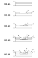
- Fig. 2A-2H are explained by sectional views of various process steps in a coating of a dielectric substrate 10 with a metallic electrode material 40, in particular a noble metal, for example gold, using a metallic conductive layer 12, for example made of copper.
- the metallic electrode material 40 can be deposited on the substrate 10, for example in the form of a conductor track. Of course, a plurality of electrodes of metallic electrode material 40 can be deposited
- a metallic conductive layer 12 is applied, in particular laminated or deposited by a coating process ( Fig. 2A ).
- the conductive layer 12 is patterned to form an exposed region 14 on the substrate 10 (FIG. Fig. 2B ).
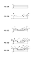
- an electrically conductive polymer layer 20 is deposited ( Fig. 2C ). Deposition on the conductor layer does not interfere if, after deposition of the metallic electrode material 40, the conductive polymer layer 20 is removed everywhere, as in FIG Figs. 2F and 2G and when the conductive polymer layer 20 shows the etching step in FIG Fig. 2G and Fig. 2H does not bother.
- the conductive layer 12 and the electrically conductive polymer layer 20 arranged in the exposed region 14 are masked with a mask made of a photoresist covering covered regions 30 of the conductive layer 12 and a region 34 of the electrically conductive polymer layer 20 and a region 32 of the electrically conductive polymer layer 20 is exposed ( Fig. 2D ).
- the conductive layer 12 is brought close to the exposed area 32 of the electrically conductive polymer layer 20 to be coated, but separated from the exposed area 32 by the areas 34 of the photoresist.
- a galvanic deposition of the metallic electrode material 40 onto the exposed regions 32 of the electrically conductive polymer layer 20 (FIG. Fig. 2E ).
- the current flow in the electrodeposition takes place substantially over the (covered) conductive layer 12 and only in the immediate vicinity of the region to be coated 32 via the electrically conductive polymer layer 20.
- relatively low electrical conductivity of the electrically conductive polymer layer 20 may be a homogeneous galvanic deposition on the exposed electrically conductive polymer layer 20 done.
- the metal of the conductive layer 12 does not come into direct contact with the deposited metallic electrode material 40, so that interdiffusion between the two metals is prevented or at least minimized.
- the excess exposed electrically conductive polymer layer 20 is removed, such as by chemical or plasma etching or chemical oxidation, or at least greatly reduced its electrical conductivity ( Fig. 2G ).
- the conductive layer 12 may then be selectively removed, eg selectively etched. This can be done with a photoresist with a negative mask to the structure of the photoresist Fig. 2D be applied.
- a portion of the conductive layer 12 may be left behind where only electrical currents are transported on the same plane of the substrate 10 and a function as an electrode is therefore not necessary. Thereby, the amount of deposited metallic electrode material 40 can be minimized. If an electrical contacting between the residual conductive layer 12 and the electrode made of metallic electrode material 40 is necessary, then the conductive layer 12 in the contact region can be locally coated with a diffusion barrier layer, for example of nickel or palladium.
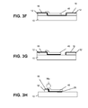
- the metallic electrode material 40 In order to electrically connect the metallic electrode material 40 to the metallic conductive layer 12, this can be done via the in the Figs. 3A-3H described process chain are generated. In this case, a diffusion into the electrode of metallic electrode material 40 is prevented or at least reduced by the application of a diffusion barrier layer 16 in the connection region. If the connection area is far away from the electrode area, eg a few millimeters, any residual diffusion that may occur can be neglected. If the diffusion barrier 16 is a metal which can be etched simultaneously with the metallic conductive layer 12 (eg Cu and Ni), then the diffusion barrier 16 can be applied over the entire area.
- a metallic conductive layer 12 is applied, ie laminated or deposited by a deposition process ( Fig. 3A ).
- the conductive layer 12 is patterned on the substrate 10 to form an exposed region 14 and a diffusion barrier layer 16, eg of nickel or palladium, is deposited on the conductive layer 12 ( Fig. 3B ).
- a diffusion barrier layer 16 eg of nickel or palladium
- This variant is favorable if the metallic electrode material 40 is to be electrically connected to the metallic conductive layer 12.
- an electrically conductive polymer layer 20 is deposited ( Fig. 3C ).
- Deposition on the metallic conductive layer 12 does not interfere with the removal of the conductive polymer layer 20 everywhere after depositing the metallic electrode material 40, as in FIG Fig. 3F, 3G and when the conductive polymer layer 20 shows the etching step in FIG Fig. 3G, 3H does not bother.
- the conductive layer 12 and the electrically conductive polymer layer 20 arranged in the exposed region 14 are masked with a mask made of a photoresist covering covered regions 30 of the conductive layer 12 and a region 34 of the electrically conductive polymer layer 20 and a region 32 of the electrically conductive polymer layer 20, as well as an area 35 of the conductive layer is exposed ( Fig. 3D ). Since perfect registration is not possible, an additional small area above the conductive layer must be exposed.
- the current flow in the electrodeposition takes place substantially over the (covered) conductive layer 12 and in the immediate vicinity of the region 32 to be coated via the electrically conductive polymer layer 20.
- electrical conductivity of the electrically conductive polymer layer 20 may be a homogeneous galvanic deposition on the exposed electrically conductive polymer layer 20 done.
- the electrodeposited electrode metal is in contact only with the conductive metal in the selective region 35.
- the diffusion of the conductive metal into the electrode metal is already minimized there by a diffusion barrier from the electrode material. Since the contact between the two metals is only very local, the contact area can be selected so that this space is very far away from the active electrode surface, so that the risk of diffusion can be further minimized.
- the excess exposed electrically conductive polymer layer 20 is removed, for example by chemical or plasma etching, or at least greatly reduced its electrical conductivity ( Fig. 3G ).
- the conductive layer 12 and the diffusion layer 16 may then be selectively removed, eg, selectively etched. This can be done with a photoresist with a negative mask to the structure of the photoresist Fig. 3D be applied.
- a part of the conductive layer 12 can remain there, where only electrical currents are transported on the same plane of the substrate 10 and a function as an electrode is therefore not necessary ( Fig. 3H ). Thereby, the amount of deposited metallic electrode material 40 can be minimized.
- the diffusion barrier layer 16 protects the conductive layer 12 locally in the contact region 16a. This area is spatially far enough away from the actual electrode area. For example, if nickel is used as the diffusion barrier layer 16, the nickel can be etched with the copper and does not disturb this last etching step. If the diffusion layer disturbs the further processes, these can be removed by selective etching of the Conductive layer to be removed. The diffusion layer remains in the interface area (16a) continue to exist.
- This embodiment is favorable if the thus coated substrate 10 is to be used not only as a biocompatible electrode but also as a carrier for components or as a cable outside the body. There is a cost advantage if only the critical areas are carried out in precious metal. The uncritical regions can be produced from the metallic conductive layer 12, which is already on the substrate 10.
- a structured galvanic structure of metal conductors (eg Au) on a dielectric base material (substrate 10) by means of a conductive polymer succeeds
- the metallic electrode material is built up only additive and the necessary use of chemistry and material is thus minimized.
Landscapes
- Chemical & Material Sciences (AREA)
- Engineering & Computer Science (AREA)
- Chemical Kinetics & Catalysis (AREA)
- Electrochemistry (AREA)
- Materials Engineering (AREA)
- Metallurgy (AREA)
- Organic Chemistry (AREA)
- Internal Circuitry In Semiconductor Integrated Circuit Devices (AREA)
- Fixed Capacitors And Capacitor Manufacturing Machines (AREA)
- Manufacturing Of Printed Wiring (AREA)
- Non-Metallic Protective Coatings For Printed Circuits (AREA)
Applications Claiming Priority (1)
| Application Number | Priority Date | Filing Date | Title |
|---|---|---|---|
| US41349310P | 2010-11-15 | 2010-11-15 |
Publications (2)
| Publication Number | Publication Date |
|---|---|
| EP2453471A2 true EP2453471A2 (fr) | 2012-05-16 |
| EP2453471A3 EP2453471A3 (fr) | 2013-05-15 |
Family
ID=44789361
Family Applications (1)
| Application Number | Title | Priority Date | Filing Date |
|---|---|---|---|
| EP11185353.7A Withdrawn EP2453471A3 (fr) | 2010-11-15 | 2011-10-17 | Procédé de séparation galvanique d'une électrode sur un substrat diélectrique |
Country Status (2)
| Country | Link |
|---|---|
| US (2) | US20120118752A1 (fr) |
| EP (1) | EP2453471A3 (fr) |
Cited By (2)
| Publication number | Priority date | Publication date | Assignee | Title |
|---|---|---|---|---|
| WO2015169495A1 (fr) * | 2014-05-05 | 2015-11-12 | Preh Gmbh | Procédé de galvanisation pour des structures en îlots |
| CN118452933A (zh) * | 2024-05-01 | 2024-08-09 | 西北工业大学 | 一种可储备导电聚合物的跨界面深孔阵列神经电极及制备方法 |
Family Cites Families (9)
| Publication number | Priority date | Publication date | Assignee | Title |
|---|---|---|---|---|
| US5300208A (en) * | 1989-08-14 | 1994-04-05 | International Business Machines Corporation | Fabrication of printed circuit boards using conducting polymer |
| US5298687A (en) * | 1990-12-27 | 1994-03-29 | Remtec, Inc. | High-density multilayer interconnection system on a ceramic substrate for high current applications and method of manufacture |
| US5427841A (en) * | 1993-03-09 | 1995-06-27 | U.S. Philips Corporation | Laminated structure of a metal layer on a conductive polymer layer and method of manufacturing such a structure |
| DE19637018A1 (de) * | 1996-09-12 | 1998-03-19 | Bayer Ag | Verfahren zur Herstellung von starren und flexiblen Schaltungen |
| JPH10215072A (ja) * | 1997-01-30 | 1998-08-11 | Nec Toyama Ltd | 多層印刷配線板の製造方法 |
| US7146221B2 (en) * | 2001-11-16 | 2006-12-05 | The Regents Of The University Of California | Flexible electrode array for artifical vision |
| DE10360624B4 (de) * | 2003-12-19 | 2007-05-03 | W.C. Heraeus Gmbh | Elektrodenstruktur, Verfahren zu ihrer Herstellung und ihre Verwendung |
| TWI270329B (en) * | 2005-04-04 | 2007-01-01 | Phoenix Prec Technology Corp | Method for fabricating conducting bump structures of circuit board |
| US20070190794A1 (en) * | 2006-02-10 | 2007-08-16 | Virgin Islands Microsystems, Inc. | Conductive polymers for the electroplating |
-
2011
- 2011-10-17 EP EP11185353.7A patent/EP2453471A3/fr not_active Withdrawn
- 2011-10-31 US US13/285,338 patent/US20120118752A1/en not_active Abandoned
-
2015
- 2015-08-07 US US14/820,755 patent/US20150345043A1/en not_active Abandoned
Non-Patent Citations (1)
| Title |
|---|
| None |
Cited By (2)
| Publication number | Priority date | Publication date | Assignee | Title |
|---|---|---|---|---|
| WO2015169495A1 (fr) * | 2014-05-05 | 2015-11-12 | Preh Gmbh | Procédé de galvanisation pour des structures en îlots |
| CN118452933A (zh) * | 2024-05-01 | 2024-08-09 | 西北工业大学 | 一种可储备导电聚合物的跨界面深孔阵列神经电极及制备方法 |
Also Published As
| Publication number | Publication date |
|---|---|
| EP2453471A3 (fr) | 2013-05-15 |
| US20120118752A1 (en) | 2012-05-17 |
| US20150345043A1 (en) | 2015-12-03 |
Similar Documents
| Publication | Publication Date | Title |
|---|---|---|
| DE2036139A1 (de) | Dunnfümmetallisierungsverfahren fur Mikroschaltungen | |
| EP1430489B1 (fr) | Composant electroceramique comportant plusieurs surfaces de contact | |
| EP2162922A1 (fr) | Structure de contact pour un composant semi-conducteur et son procédé de fabrication | |
| DE2648274A1 (de) | Verfahren zum selektiven elektroplattieren eines bereiches einer oberflaeche | |
| DE102007005161B4 (de) | Verfahren zur Metallisierung von Substraten | |
| DE69935333T2 (de) | Verbessertes verfahren zur herstellung leitender spuren und so hergestellte gedruckte leiterplatten | |
| DE102014206558B4 (de) | Verfahren zum Herstellen eines MID-Schaltungsträgers und MID-Schaltungsträger | |
| EP2453471A2 (fr) | Procédé de séparation galvanique d'une électrode sur un substrat diélectrique | |
| EP0764334B1 (fr) | Procede de fabrication de composants a base de film metallique | |
| DE102008034616A1 (de) | Prägefolie und deren Verwendung sowie Verfahren zur Herstellung von Strukturelementen aus Kupfer | |
| WO2014079657A1 (fr) | Procédé de réalisation d'une zone de connexion d'une puce de semi-conducteur optoélectronique | |
| WO2010097230A2 (fr) | Procédé de réalisation d'une structure métallique sur un substrat | |
| WO2015185412A1 (fr) | Procédé de production d'un ensemble de feuilles et ensemble de feuilles correspondant | |
| DE102014103293B4 (de) | Halbleitervorrichtung und Herstellungsverfahren dafür | |
| WO2015044022A1 (fr) | Procédé de création de motifs sur des couches de matériaux oxydables au moyen de l'oxydation et substrat pourvu d'un tel revêtement à motifs | |
| WO2011042197A1 (fr) | Procédé de fabrication d'une carte de circuit imprimé, notamment d'une carte de circuit imprimé multicouche | |
| EP1707037A1 (fr) | Procede de fabrication d'un element de carte de circuits imprimes et element de carte de circuits imprimes | |
| WO2022129230A1 (fr) | Procédé d'assemblage de nanostratifiés par électrodéposition | |
| EP1502299B1 (fr) | Etablissement des contacts de nanotubes | |
| DE102021126402B4 (de) | Verfahren zum Herstellen elektrisch leitfähiger Strukturen | |
| WO2015067792A1 (fr) | Grille de connexion et son utilisation | |
| DE102009040632B4 (de) | Halbleiter-Bauelement und Verfahren zum Herstellen eines Halbleiter-Bauelements und damit hergestelltes Halbleiter-Bauelement | |
| DE102012213555A1 (de) | Verfahren zur Herstellung eines Substrats für ein Leistungshalbleiterbauelement und Substrat | |
| DE102018114801A1 (de) | Diffusionsbarriere für implantierbare Elektrodenleitungen | |
| DE102007029820B4 (de) | Verfahren zur Aufbringung metallischer Stützstrukturen auf Elektroden von Leuchtdioden aus organischen Materialien |
Legal Events
| Date | Code | Title | Description |
|---|---|---|---|
| PUAI | Public reference made under article 153(3) epc to a published international application that has entered the european phase |
Free format text: ORIGINAL CODE: 0009012 |
|
| AK | Designated contracting states |
Kind code of ref document: A2 Designated state(s): AL AT BE BG CH CY CZ DE DK EE ES FI FR GB GR HR HU IE IS IT LI LT LU LV MC MK MT NL NO PL PT RO RS SE SI SK SM TR |
|
| AX | Request for extension of the european patent |
Extension state: BA ME |
|
| PUAL | Search report despatched |
Free format text: ORIGINAL CODE: 0009013 |
|
| AK | Designated contracting states |
Kind code of ref document: A3 Designated state(s): AL AT BE BG CH CY CZ DE DK EE ES FI FR GB GR HR HU IE IS IT LI LT LU LV MC MK MT NL NO PL PT RO RS SE SI SK SM TR |
|
| AX | Request for extension of the european patent |
Extension state: BA ME |
|
| RIC1 | Information provided on ipc code assigned before grant |
Ipc: H01L 21/48 20060101AFI20130409BHEP Ipc: H01L 23/498 20060101ALI20130409BHEP Ipc: A61N 1/05 20060101ALI20130409BHEP |
|
| STAA | Information on the status of an ep patent application or granted ep patent |
Free format text: STATUS: THE APPLICATION IS DEEMED TO BE WITHDRAWN |
|
| 18D | Application deemed to be withdrawn |
Effective date: 20131116 |