EP2458633A2 - Système semi-conducteur de puissance - Google Patents
Système semi-conducteur de puissance Download PDFInfo
- Publication number
- EP2458633A2 EP2458633A2 EP11185539A EP11185539A EP2458633A2 EP 2458633 A2 EP2458633 A2 EP 2458633A2 EP 11185539 A EP11185539 A EP 11185539A EP 11185539 A EP11185539 A EP 11185539A EP 2458633 A2 EP2458633 A2 EP 2458633A2
- Authority
- EP
- European Patent Office
- Prior art keywords
- power semiconductor
- wall element
- metal
- semiconductor system
- opening
- Prior art date
- Legal status (The legal status is an assumption and is not a legal conclusion. Google has not performed a legal analysis and makes no representation as to the accuracy of the status listed.)
- Granted
Links
Images



Classifications
-
- H—ELECTRICITY
- H10—SEMICONDUCTOR DEVICES; ELECTRIC SOLID-STATE DEVICES NOT OTHERWISE PROVIDED FOR
- H10W—GENERIC PACKAGES, INTERCONNECTIONS, CONNECTORS OR OTHER CONSTRUCTIONAL DETAILS OF DEVICES COVERED BY CLASS H10
- H10W40/00—Arrangements for thermal protection or thermal control
- H10W40/40—Arrangements for thermal protection or thermal control involving heat exchange by flowing fluids
-
- H—ELECTRICITY
- H10—SEMICONDUCTOR DEVICES; ELECTRIC SOLID-STATE DEVICES NOT OTHERWISE PROVIDED FOR
- H10W—GENERIC PACKAGES, INTERCONNECTIONS, CONNECTORS OR OTHER CONSTRUCTIONAL DETAILS OF DEVICES COVERED BY CLASS H10
- H10W40/00—Arrangements for thermal protection or thermal control
- H10W40/40—Arrangements for thermal protection or thermal control involving heat exchange by flowing fluids
- H10W40/47—Arrangements for thermal protection or thermal control involving heat exchange by flowing fluids by flowing liquids, e.g. forced water cooling
-
- H—ELECTRICITY
- H05—ELECTRIC TECHNIQUES NOT OTHERWISE PROVIDED FOR
- H05K—PRINTED CIRCUITS; CASINGS OR CONSTRUCTIONAL DETAILS OF ELECTRIC APPARATUS; MANUFACTURE OF ASSEMBLAGES OF ELECTRICAL COMPONENTS
- H05K7/00—Constructional details common to different types of electric apparatus
- H05K7/20—Modifications to facilitate cooling, ventilating, or heating
-
- H—ELECTRICITY
- H05—ELECTRIC TECHNIQUES NOT OTHERWISE PROVIDED FOR
- H05K—PRINTED CIRCUITS; CASINGS OR CONSTRUCTIONAL DETAILS OF ELECTRIC APPARATUS; MANUFACTURE OF ASSEMBLAGES OF ELECTRICAL COMPONENTS
- H05K7/00—Constructional details common to different types of electric apparatus
- H05K7/20—Modifications to facilitate cooling, ventilating, or heating
- H05K7/20218—Modifications to facilitate cooling, ventilating, or heating using a liquid coolant without phase change in electronic enclosures
- H05K7/20254—Cold plates transferring heat from heat source to coolant
-
- H—ELECTRICITY
- H05—ELECTRIC TECHNIQUES NOT OTHERWISE PROVIDED FOR
- H05K—PRINTED CIRCUITS; CASINGS OR CONSTRUCTIONAL DETAILS OF ELECTRIC APPARATUS; MANUFACTURE OF ASSEMBLAGES OF ELECTRICAL COMPONENTS
- H05K7/00—Constructional details common to different types of electric apparatus
- H05K7/20—Modifications to facilitate cooling, ventilating, or heating
- H05K7/2089—Modifications to facilitate cooling, ventilating, or heating for power electronics, e.g. for inverters for controlling motor
- H05K7/20927—Liquid coolant without phase change
Definitions
- the present invention relates to a power semiconductor system based on known power semiconductor modules.
- Power semiconductor modules are known in various embodiments.
- a substrate having a power semiconductor circuit and a chassis are assembled into a power semiconductor module. It is important to ensure that the heat transfer between power semiconductor circuit, body and a heat sink arranged for this purpose, the desired removal of waste heat from the power semiconductor circuit is ensured, and that a simple, preferably automated, mounting of the power semiconductor module is possible.
- a power semiconductor module for mounting on a heat sink, wherein the power semiconductor module has a metallic base body, which forms a trough and encloses a disposed therein, a power semiconductor circuit supporting substrate on five sides.
- the main body is preferably made of copper because of its excellent thermal conductivity.
- the main body can be connected directly by way of example by means of an adhesive or screw connection with a heat sink.
- a disadvantage of such a power semiconductor module is due to the connection between the base plate and heat sink, sub-optimal heat transfer from the power semiconductor circuit to the heat sink.
- the object of the invention is to present an improved power semiconductor system in which efficient heat transfer from the power semiconductor circuit to a cooling medium is possible.
- the present disclosure proposes to arrange a power semiconductor circuit on an outer wall of a wall element whose inner wall forms a liquid-tight or gas-tight wall of a line system which is provided for cooling the semiconductor circuit and which conducts a fluid working medium. As a result, excellent cooling of the power semiconductor circuit is achieved.
- the power semiconductor system has a line system for a fluid working medium - for example, a cooling liquid or a cooling gas - on.
- the conduit system may be a closed conduit system or may form a conduit system closed except for an inlet port and an outlet port. As a result, an undesirable escape of the working medium is prevented.
- the inlet and outlet openings can be arranged on the same side, preferably an end face of the metal molding.
- the inlet and outlet ports may serve to connect the piping to a pump system.
- the conduit system may be connected to a pumping system to pump the working fluid through the conduit system. In this case, the line system can form a closed line system with the pump system.
- a circulation of the working medium within the conduit system for the removal of heat can be passive either due to the heating of the working medium - for example in the form of a thermosyphon or a so-called heat pipe - as well as active - for example by a pump system as described above.
- the working medium can be chosen freely.
- the working medium may be gaseous or liquid under normal conditions. Suitable working media are known to those skilled in thermosyphon and heat pipes. These include, inter alia, water, oil, ethanol, acetone and ammonia or mixtures thereof.
- the working medium can change between a liquid and a gaseous state.
- the power semiconductor system has a wall member having an outside and an inside.
- the outside can essentially be considered a conduit system opposite side of the wall element and the inside are understood as a line of the system substantially facing side of the wall element.
- the inside and the outside of the wall element may form the main surfaces of the wall element.
- the inner and outer sides can be designed-either individually-plan or structured.
- the top may include at least one structural element for mounting a power semiconductor circuit.
- the wall element may be plate-shaped or substantially plate-shaped or at least have a substantially plate-shaped portion which forms an essential element of the wall element.
- essential is to be understood that the described functionality of the wall element - if this functionality is not optional for the respective embodiment of the wall element - is at least partially ensured by the element or the section.
- a distance between the inside and outside of the wall element in relation to the length of the wall element is small, for example less than 10% or less than 5% of the length of the wall element.
- a distance between the inside and outside of the wall member in relation to the length of the plate-shaped portion is small, for example, less than 10% or less than 5% of the length of the plate-shaped portion. This at least partially small distance a good thermal conductivity between the inside and outside is achieved. By a, at least partially, plate-like shape is achieved with low material consumption, a good ratio between the heat transfer surface and the distance between the inside and outside.
- the power semiconductor system has a power semiconductor circuit arranged on the outside of the wall element.
- a simple and / or automated and / or secure installation of the power semiconductor circuit on the outside of the wall element can be favored.
- the wall element can impart stability to the power semiconductor circuit which protects the power semiconductor circuit in later assembly of the wall element with the conduit system. This is especially true when a power semiconductor circuit after starting the power semiconductor circuit, i. on site, to be replaced.
- a power semiconductor circuit according to the present disclosure may comprise a circuit having at least one semiconductor device with a nominal voltage of over 100 V or even over 600 V.
- a power semiconductor circuit according to the present disclosure may be a circuit with which a current path between a first potential and a second potential is selectively switched between a substantially closed (low resistance) state and a substantially open (high resistance) state in response to at least one control signal can be, wherein a difference between the first potential and the second potential is more than 100 V or even more than 600 V, or wherein a regularly flowing in the closed state over the current path current is more than 100 A or even more than 1000 A.
- the inside of the wall member forms a liquid-tight wall of the conduit system.
- the power semiconductor circuit is arranged very close to a fluid working medium provided in the line system, whereby the heat transfer between the power semiconductor circuit and the fluid working medium and consequently also the removal of the heat generated in the power semiconductor circuit waste heat is promoted.
- the inside of the wall element is to form a gastight wall of the conduit system or merely a liquid-tight wall of the conduit system depends on the working medium used and on the expected operating conditions. If it is to be expected that the working medium can assume a gaseous state, the inside of the wall element should have gas-tightness.
- the power semiconductor system may comprise a metal shaped body, for example a metal shaped body produced wholly or partly from copper and / or aluminum, which is a structure separate or separable from the wall element.
- a metal shaped body for example a metal shaped body produced wholly or partly from copper and / or aluminum, which is a structure separate or separable from the wall element.
- the shaped metal body and the wall element are made of the same material, preferably aluminum.
- the wall element may be non-positively and / or positively secured to the metal moldings.
- known screw, snap snap connections or compounds that are formed by deformation of a portion of the wall member and / or the metal molding are preferred.
- metal is a suitable material for dissipating waste heat that has been transported from a power semiconductor circuit to the metal mold due to, for example, a temperature gradient.
- the metal molding may be formed as a heat sink, for example as a ribbed heat sink.
- the line system can be arranged in and / or on the metal molding.
- a shaped metal body is often - regardless of whether the working fluid is liquid or gaseous - referred to as a liquid-cooled heat sink and is able to carry away large amounts of waste heat from the metal moldings, since the working medium serves as a heat transfer medium.
- a part of the conduit system can be formed by cavities in the metal molding - for example by bores. As a result, a transfer of heat from the metal molding to the working medium is favored.
- the metal molding may also have a recess in which a capacitor is arranged, which is electrically insulated from the metal molding by means of a potting material. In this way, the metal molding can serve as a heat sink and / or as a carrier for various power semiconductor components.
- the metal molding may have a first cavity forming part of the pipe system having an opening on at least one surface of the metal molding.
- the wall element can be mounted on the metal molding in such a way that the inside of the wall element closes the opening in a liquid-tight or gas-tight manner.
- a cavity can be easily produced, for example, by using a corresponding mold for producing the metal molding or by drilling or milling a metal molding.
- the opening can be closed due to the liquid or gas tightness of the inside of the wall element.
- the inside of the wall element completely cover the opening and seal the opening to the outside by direct contact with the metal mold body along the entire circumference of the opening, preferably by means of an elastic sealing member along liquid- or gas-tight.
- the wall element can rest on an outer surface of the metal molding or can produce a gas-tight or liquid-tight connection with the metal molding within the opening, for example along a web provided on the inner circumference of the opening. Consequently, the opening, together with other cavities provided in the metal mold, forms part of the piping system. A working fluid flowing into the first cavity may come into direct contact with the inside of the wall member.
- the power semiconductor system may comprise an elastic sealing element, for example an O-ring.
- the sealing element - which can also be formed from many individual sealing elements - can cooperate with the wall element - for example with the inside of the wall element - to a like
- the wall element may be secured to the metal mold and the gasket may notoriously be clamped between the wall element and the metal mold and disposed around the opening such that the opening is sealed in a liquid or gas tight manner.
- the sealing element may be arranged in the region of an inner circumference of the opening.
- the sealing member may extend around the opening adjacent a periphery of the opening, for example along a ridge provided at the inner circumference of the opening.
- the sealing element can be inside or outside the opening.
- the above-mentioned first cavity in the metal molding may include a first opening connected to an inlet side portion of the piping and / or a second opening connected to an outlet side portion of the piping.
- the cavity may have an elongate shape in which the first opening is located at an outermost third and the second opening is located in an outermost third of the length of the cavity in one of the first opening.
- Each of the first and second openings may extend over more than 60% or more than 80% of the width of the cavity.
- the inlet side and / or the outlet side portion of the conduit system may each be formed by a single bore.
- the inlet-side and / or the outlet-side portion of the conduit system may be formed by a bore in the metal shaped body, which extends transversely to the length of the first cavity. Consequently, the first or second opening can be produced by milling the cavity to a hole in a surface of the metal molding. At the interface between the cavity and the bore creates the first or second bore without further action.
- Several cavities can be formed parallel to each other in the metal mold body in such a way that the cavities are offset from one another only with respect to their longitudinal axes. In this way, a single bore may act as an inlet or outlet side portion of the conduit system for all cavities.
- the metal molding may have an inlet opening and an outlet opening.
- the conduit system may extend in a fluid-tight or gas-tight manner between the inlet opening and the outlet opening.
- the metal shaped article has a defined inlet opening and a defined outlet opening.
- the metal molding may have only a single inlet opening and / or only a single outlet opening. This also makes it easier to ensure the liquid or gas tightness of the conduit system. Whether the pipe system should extend gas-tight or only liquid-tight between the inlet opening and the outlet opening depends on the working medium used and on the expected operating conditions. If it is to be expected that the working fluid can assume a gaseous state, the piping system should have gas-tightness.
- the power semiconductor system may have a frame attached to the metal moldings.
- the frame can fasten the wall element non-positively and / or positively on the metal moldings.
- the frame may press the wall element against the metal mold.
- the use of a frame allows a simultaneous application of force to different locations of the wall element. This can reduce the likelihood of deleterious mechanical deformation of the power divider circuit disposed on the wall element.
- the frame may be made of an electrically insulating material - for example, plastic - be.
- the frame can also be - at least for the most part - made of an electrically conductive material, for example metal, which is electrically insulated from the current-carrying elements of the power semiconductor circuit by means of an electrically insulating material.
- the frame may be formed so that the frame rests only in an outer edge region of the outer side of the wall element on the wall element.
- the frame can be fastened to the metal molding by means of an automatically producible connection, for example by means of a screw connection or a snap connection. As a result, an automated assembly of the wall element and the frame is favored.
- the current-carrying elements of the power semiconductor circuit may be electrically insulated from the inside of that wall element on which the power semiconductor circuit is arranged. In this way it is avoided that an unwanted current path between the power semiconductor circuit and another Element of the power semiconductor system - for example, the metal moldings and / or the working medium - arises.
- the power semiconductor circuit may comprise a substrate equipped with power semiconductors in a specialized manner.
- the metallic heat sink of the wall element may be designed as a simple metal plate or as a metal plate with cooling fins or cooling pins projecting perpendicular or substantially perpendicular to a main surface of the metal surface.
- the cooling fins and / or the cooling pins can cause an enlargement of a heat-emitting surface of the heat sink.
- the line system can be filled with a fluid working medium.
- the working medium may be the inside of the wall element in contact with the working medium.
- the power semiconductor system may have a plurality of first cavities as described above.
- the power semiconductor system may have a plurality of wall elements as described above. Several or all of the individual cavities formed on at least one surface of the metal mold body by the individual cavities may be closed in a liquid-tight or gas-tight manner by a single wall element. Nevertheless, individual ones of the individual openings can be closed in liquid-tight or gas-tight manner by individual wall elements.
- the power semiconductor system may have a frame as described above, which presses a plurality of wall elements - for example in the manner described above - against the metal molding.
- FIG. 1 a perspective view of a metal shaped body for a power semiconductor system according to a first embodiment
- FIG. 2 a perspective view of a power semiconductor system according to a second embodiment
- FIG. 3 a perspective view of a power semiconductor system according to a third embodiment
- FIG. 4 a power semiconductor system according to a fourth embodiment
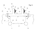
- FIG. 5 a schematic sectional view of a power semiconductor system according to a fourth embodiment.
- FIG. 6 a schematic sectional view of a power semiconductor system according to a sixth embodiment.
- the FIG. 1 shows a perspective view of a metal shaped body 40 for a power semiconductor system 100 according to a first embodiment.
- the metal shaped body is shown as a heat sink for a power semiconductor circuit, which can be cooled by a fluid working medium.
- the metal molding 40 has a plurality of approximately rectangular cavities 41 and a plurality of openings 42 of these.
- the inlet opening is connected via the respective openings 42 with the respective cavities 41 of the metal shaped body 40 such that the cavities 41 with the inlet opening 13 form a conduit system 10 for the fluid working medium.
- the openings 43, over which - similar to the openings 42 - the cavities 41 for the fluid working medium are connected to the outlet opening 14 are in the FIG.
- a respective sealing element 50 is arranged, which with a power semiconductor circuit 30 supporting, in the FIG. 1 not shown wall member 20 cooperates to liquid-tight or gas-tight to close the respective openings which form the respective cavities 41 in the upper surface of the metal molding.
- the FIG. 2 shows a perspective view of a power semiconductor system 100 according to a second embodiment.
- the in the FIG. 2 embodiment shown also has a like in the FIG. 1 shown metal moldings 40 with the features described above. That in the FIG. 2 shown power semiconductor system 100 also has a plurality of wall elements 20. At the the metal moldings 40th remote from the outside of the respective wall element 20, a power semiconductor circuit 30 is arranged.
- Each of the wall elements 20 covers one of the in the representation of FIG. 2 because of the cover by the respective wall element 20 not visible cavity 41, whereby the respective opening which forms the respective covered cavity 41 in the upper surface of the metal molding 40, liquid-tight or gas-tight to close.
- FIG. 3 shows a perspective view of a power semiconductor system 100 according to a third embodiment.
- the in the FIG. 3 embodiment shown also has a as in the FIG. 2 shown power semiconductor system 100 with the features described above. That in the FIG. 3 shown power semiconductor system 100 additionally has a plastic frame 60 which is fixed to the metal molding 40.
- the plastic frame 60 surrounds - in the FIG. 3 not visible - individual wall elements 20 such that the respective outer side of the individual wall elements 20 only slightly - for example, less than 10% or less than 5% - is covered by the plastic frame.
- the plastic frame 60 presses the wall members 20 against the sealing members 50 in the direction of the metal formed body 40, whereby the wall members 20 cooperate with the sealing members 50 to liquid or gas tight seal the openings formed by the cavity 41 in the upper surface of the metal mold body 40 ,
- the use of a single frame 60 simplifies assembly.
- FIG. 4 shows a schematic exploded view of a power semiconductor system 100 according to a fourth embodiment.
- an additional capacitor module with an unhoused capacitor 84 and a spacer 82 made of an electrically insulating material for the arrangement of the capacitor 84 in a recess 80 of the metal shaped body 40 is additionally provided here.
- a casting compound for electrical insulation of the capacitor 84 relative to the metal molding 40, is additionally provided in the depression 80.
- this capacitor 84 can be cooled simultaneously with the power circuits.
- the immediate possibility of connecting the capacitor 84 with its connection elements 86 to those connection elements 36 of the power circuit 30 assigned to them is likewise recognizable.
- the respective connection elements 36 are constructed and arranged relative to one another such that a welded connection can be formed.
- the power semiconductor system 100 has sufficient free space to be able to reach the two connection elements 36, 86 with a welding device.
- connection elements 86 of the capacitor 84 and the associated connection elements 36 of the power circuit 30 are not permanently connected to one another in a materially cohesive manner, but are releasably connected, preferably non-positively.
- the metal molding 40 has a further recess 48 to arrange an unillustrated external connector there and this and each circuit to connect with other connection elements 38 of the power circuit 30. It is preferred if this recess 48 is provided laterally to the power circuits 40 and the associated wall elements 20 relative to the capacitor 84. This recess 48 extends from that main side of the metal molding 40 on which the wall elements 20 are provided to the opposite main side.
- FIG. 5 shows a schematic sectional view of a power semiconductor system 100 according to a fifth embodiment.
- the illustrated power semiconductor system 100 comprises a line system 10, a wall element 20, a plurality of power semiconductor circuits 30, a metal shaped body 40 and a sealing element 50.
- the piping system 10 is configured to guide a fluid working medium serving as a cooling liquid, and has an inlet-side portion 11 and an outlet-side portion 12, each with a in the FIG. 4 not shown inlet and outlet ports 13, 14 are connected.
- the wall element 20 has an outer side 21, which faces away from the line system, and an inner side 22 which essentially faces the line system.
- the wall element 20 has a metallic heat sink 23, which is shown in FIG illustrated embodiment, the inner side 22 of the wall member 20 forms, and a plurality of substrates 31.
- the heat sink 23 has projections 25 that project perpendicularly from the main surface of the outer side 21 of the wall element 20 and on which the substrates 31 are arranged.
- Each of the power semiconductor circuits 30 has a substrate 31 equipped with power semiconductors, which has a ceramic plate 24 in order to electrically isolate the substrate 31 from the heat sink 23.
- the metal molding 40 has a first cavity 41, which forms part of the conduit system 10.
- the cavity 41 may be formed by milled the metal moldings 40 or manufactured in a corresponding mold.
- the cavity 41 has a first opening 42 through which the fluid working fluid can flow between the cavity 41 and the inlet-side portion 11, and a second opening 43 through which the fluid working fluid can flow between the cavity 41 and the outlet-side portion 12.
- the inlet and outlet sections 11, 12 may be formed in a simple manner by respective holes in the metal moldings.
- the first and second openings 42, 43 can be formed in a simple manner in that the holes dne cavity 41 partly cut.
- the sealing element 50 is arranged between the inner side 22 of the wall element 20 and the metal molding 40.
- the wall element is fastened by means of screws 70 to the metal molding 40.
- the sealing member cooperates with the inner side 22 of the wall member 20 in a technical manner to seal the opening formed by the cavity 41 in the upper surface of the metal mold body 40 liquid-tight or gas-tight.
- the inner side 22 of the wall element 20 forms a wall of the conduit system 10.
- FIG. 6 shows a schematic sectional view of a power semiconductor system 100 according to a sixth embodiment.
- the power semiconductor system 100 shown has a line system 10, a wall element 20, a plurality of power semiconductor circuits 30, a metal mold 40, a sealing element 50 and a frame 60.
- the conduit system 10 is designed to guide a fluid working medium serving as cooling fluid and has an inlet-side section 11 and a outlet-side section 12, which are each connected to an inlet or outlet opening 13, 14.
- the wall element 20 has an outer side 21 facing away from the line system and an inner side 22 substantially facing the line system.
- the wall element 20 has a metallic heat sink 23, the embodiment illustrated here forms the inner side 22 of the wall element 20.
- the heat sink 23 has pins 26 which project perpendicularly from the main surface of the inner side 22 of the wall element 20 and which enlarge the heat-emitting surface of the inner side 22 of the wall element 20.
- Each of the power semiconductor circuits 30 has a substrate 31 equipped with power semiconductors, which has a ceramic plate 24 with respect to the heat sink 23 for the purpose of electrical insulation.
- the shaped metal body 40 has a cavity 41, which forms part of the conduit system 10.
- This cavity 41 can be formed by milling the metal shaped body 40 accordingly or producing it in a corresponding casting mold.
- the cavity 41 has a first opening 42 through which the fluid working fluid can flow between the cavity 41 and the inlet-side portion 11, and a second opening 43 through which the fluid working fluid can flow between the cavity 41 and the outlet-side portion 12.
- the inlet and outlet sections 11, 12 may be formed in a simple manner by respective holes in the metal moldings.
- the first and second openings 42, 43 can be formed in a simple manner in that the holes partially cut the cavity 41.
- the sealing element 50 is arranged between the inner side 22 of the wall element 20 and the metal molding 40.
- the sealing member cooperates with the inner side 22 of the wall member 20 in a technical manner to seal the opening formed by the cavity 41 in the upper surface of the metal molding 40 liquid-tight or gas-tight.
- the inner side 22 of the wall element 20 forms a wall of the conduit system 10.
- the frame 60 which may be made of a non-conductive material and secured by screws 70 on the metal moldings, attaches the wall element 20 to the metal moldings 40. In this case, the frame 60 presses against the outside 21 of Wall element 20 and is located only in an outer edge region of the outer side 21 of the wall member 20 on the wall element 20.
Landscapes
- Engineering & Computer Science (AREA)
- Microelectronics & Electronic Packaging (AREA)
- Physics & Mathematics (AREA)
- Thermal Sciences (AREA)
- Cooling Or The Like Of Semiconductors Or Solid State Devices (AREA)
- Cooling Or The Like Of Electrical Apparatus (AREA)
- Dc-Dc Converters (AREA)
Applications Claiming Priority (1)
| Application Number | Priority Date | Filing Date | Title |
|---|---|---|---|
| DE102010043446A DE102010043446B3 (de) | 2010-11-05 | 2010-11-05 | Leistungshalbleitersystem |
Publications (3)
| Publication Number | Publication Date |
|---|---|
| EP2458633A2 true EP2458633A2 (fr) | 2012-05-30 |
| EP2458633A3 EP2458633A3 (fr) | 2013-01-23 |
| EP2458633B1 EP2458633B1 (fr) | 2016-12-14 |
Family
ID=44799857
Family Applications (1)
| Application Number | Title | Priority Date | Filing Date |
|---|---|---|---|
| EP11185539.1A Active EP2458633B1 (fr) | 2010-11-05 | 2011-10-18 | Système semi-conducteur de puissance |
Country Status (7)
| Country | Link |
|---|---|
| US (1) | US8730672B2 (fr) |
| EP (1) | EP2458633B1 (fr) |
| JP (1) | JP5827873B2 (fr) |
| KR (1) | KR101934592B1 (fr) |
| CN (1) | CN102456642B (fr) |
| BR (1) | BRPI1106709A2 (fr) |
| DE (1) | DE102010043446B3 (fr) |
Cited By (1)
| Publication number | Priority date | Publication date | Assignee | Title |
|---|---|---|---|---|
| EP3996133A4 (fr) * | 2019-07-02 | 2022-07-13 | Mitsubishi Electric Corporation | Module de puissance et son procédé de fabrication |
Families Citing this family (39)
| Publication number | Priority date | Publication date | Assignee | Title |
|---|---|---|---|---|
| DE102010043445B3 (de) * | 2010-11-05 | 2012-04-19 | Semikron Elektronik Gmbh & Co. Kg | Kondensatoranordnung, leistungselektronisches Gerät damit undVerfahren zur Herstellung der Kondensatoranordnung |
| JP5508357B2 (ja) | 2011-07-29 | 2014-05-28 | 日立オートモティブシステムズ株式会社 | 電力変換装置 |
| DE102012201766B4 (de) | 2012-02-07 | 2019-06-13 | Semikron Elektronik Gmbh & Co. Kg | Leistungselektronisches System mit einem mindestens einen Einzug aufweisenden Gehäuse |
| EP2830073B1 (fr) * | 2012-03-19 | 2017-09-13 | Mitsubishi Electric Corporation | Appareil convertisseur de puissance |
| JPWO2014020806A1 (ja) * | 2012-08-03 | 2016-07-21 | 富士電機株式会社 | 冷却構造体及び電力変換装置 |
| JP6034957B2 (ja) * | 2013-04-04 | 2016-11-30 | 本田技研工業株式会社 | 冷却構造体 |
| RU2522937C1 (ru) * | 2013-04-25 | 2014-07-20 | Открытое акционерное общество "Т-Платформы" | Система жидкостного охлаждения многопроцессорного вычислительного комплекса, сборка и теплоотводящий модуль |
| DE102013109532B3 (de) * | 2013-09-02 | 2014-08-28 | Semikron Elektronik Gmbh & Co. Kg | Leistungshalbleitereinrichtung |
| DE102013109592B3 (de) * | 2013-09-03 | 2014-10-23 | Semikron Elektronik Gmbh & Co. Kg | Leistungshalbleitereinrichtung |
| DE102013109589B3 (de) | 2013-09-03 | 2015-03-05 | Semikron Elektronik Gmbh & Co. Kg | Leistungshalbleitereinrichtung und Verfahren zur Herstellung einer Leistungshalbleitereinrichtung |
| DE102013110815B3 (de) * | 2013-09-30 | 2014-10-30 | Semikron Elektronik Gmbh & Co. Kg | Leistungshalbleitereinrichtung und Verfahren zur Herstellung einer Leistungshalbleitereinrichtung |
| DE102013110812B3 (de) | 2013-09-30 | 2014-10-09 | Semikron Elektronik Gmbh & Co. Kg | Verfahren zur Herstellung eines weitergebildeten Metallformkörpers und Verfahren zur Herstellung einer Leistungshalbleitereinrichtung mit einer Lotverbindung diesen weitergebildeten Metallformkörper verwendend. |
| US9913404B2 (en) * | 2014-06-24 | 2018-03-06 | Mitsubishi Electric Corporation | Cooling apparatus |
| DE102014214209B4 (de) * | 2014-07-22 | 2016-05-04 | Siemens Aktiengesellschaft | Kühlvorrichtung zur zielgerichteten Kühlung von elektronischen und/oder elektrischen Bauelementen, Umrichter mit einer derartigen Kühlvorrichtung sowie Elektro- oder Hybridfahrzeug mit einem derartigen Umrichter |
| DE102014112516B3 (de) * | 2014-09-01 | 2015-12-24 | Semikron Elektronik Gmbh & Co. Kg | Leistungselektronisches System mit Flüssigkeitskühleinrichtung und Verfahren zur Herstellung der Flüssigkeitskühleinrichtung |
| KR101646375B1 (ko) * | 2014-11-05 | 2016-08-12 | 현대자동차주식회사 | 차량용 인덕터장치 |
| CN105742252B (zh) * | 2014-12-09 | 2019-05-07 | 台达电子工业股份有限公司 | 一种功率模块及其制造方法 |
| JP6885126B2 (ja) * | 2017-03-22 | 2021-06-09 | 富士電機株式会社 | インバータ装置 |
| KR101950442B1 (ko) * | 2017-04-28 | 2019-02-20 | 엘에스산전 주식회사 | 서브모듈 |
| US10850623B2 (en) | 2017-10-30 | 2020-12-01 | Sf Motors, Inc. | Stacked electric vehicle inverter cells |
| KR102120221B1 (ko) * | 2018-02-21 | 2020-06-08 | 오세윤 | 열전소자를 이용하는 급속 냉각 장치 |
| US10790758B2 (en) | 2018-03-08 | 2020-09-29 | Chongqing Jinkang New Energy Vehicle Co., Ltd. | Power converter for electric vehicle drive systems |
| US10756649B2 (en) | 2018-03-23 | 2020-08-25 | Chongqing Jinkang New Energy Vehicle Co., Ltd. | Inverter module having multiple half-bridge modules for a power converter of an electric vehicle |
| US10779445B2 (en) | 2018-03-23 | 2020-09-15 | Chongqing Jinkang New Energy Vehicle Co., Ltd. | Inverter module having multiple half-bridge modules for a power converter of an electric vehicle |
| US10236791B1 (en) | 2018-03-23 | 2019-03-19 | Sf Motors, Inc. | Inverter module having multiple half-bridge modules for a power converter of an electric vehicle |
| US10772242B2 (en) | 2018-04-17 | 2020-09-08 | Chongqing Jinkang New Energy Vehicle Co., Ltd. | Inverter module of an electric vehicle |
| US10778117B2 (en) | 2018-04-17 | 2020-09-15 | Chongqing Jinkang New Energy Vehicle Co., Ltd. | Inverter module of an electric vehicle |
| US10600578B2 (en) | 2018-04-26 | 2020-03-24 | Sf Motors, Inc. | Electric vehicle inverter module capacitors |
| US10600577B2 (en) | 2018-04-26 | 2020-03-24 | Sf Motors, Inc. | Electric vehicle inverter module capacitors |
| US10660242B2 (en) | 2018-04-26 | 2020-05-19 | Chongqing Jinkang New Energy Vehicle Co., Ltd. | Electric vehicle inverter module heat sink |
| US10608423B2 (en) | 2018-04-26 | 2020-03-31 | Sf Motors, Inc. | Electric vehicle inverter module laminated bus bar |
| US10900412B2 (en) | 2018-05-31 | 2021-01-26 | Borg Warner Inc. | Electronics assembly having a heat sink and an electrical insulator directly bonded to the heat sink |
| DE102018115515A1 (de) * | 2018-06-27 | 2020-01-02 | Valeo Siemens Eautomotive Germany Gmbh | Stromrichter für ein elektrisch antreibbares Fahrzeug |
| DE102019200142A1 (de) * | 2019-01-08 | 2020-07-09 | Volkswagen Aktiengesellschaft | Kühleinheit zur Abfuhr von Abwärme von zumindest einem Leistungsbauteil |
| DE102019122511A1 (de) * | 2019-08-21 | 2021-02-25 | Seg Automotive Germany Gmbh | Stromrichtereinheit und elektrische Maschine |
| WO2021140547A1 (fr) * | 2020-01-06 | 2021-07-15 | 東芝三菱電機産業システム株式会社 | Unité de conversion de puissance électrique |
| CN112739113A (zh) * | 2020-12-30 | 2021-04-30 | 江苏中翼汽车新材料科技有限公司 | Obd压铸合金水冷散热壳体及其浇注系统 |
| CN114096123A (zh) * | 2021-11-15 | 2022-02-25 | 合众新能源汽车有限公司 | 冷却装置、冷却系统、车辆及冷却方法 |
| US12122251B2 (en) * | 2022-09-28 | 2024-10-22 | BorgWarner US Technologies LLC | Systems and methods for bidirectional message architecture for inverter for electric vehicle |
Citations (1)
| Publication number | Priority date | Publication date | Assignee | Title |
|---|---|---|---|---|
| DE102005037522A1 (de) | 2005-08-09 | 2007-02-15 | Semikron Elektronik Gmbh & Co. Kg | Leistungshalbleitermodul mit wannenförmigem Grundkörper |
Family Cites Families (24)
| Publication number | Priority date | Publication date | Assignee | Title |
|---|---|---|---|---|
| US5436793A (en) * | 1993-03-31 | 1995-07-25 | Ncr Corporation | Apparatus for containing and cooling an integrated circuit device having a thermally insulative positioning member |
| JP2000340727A (ja) * | 1999-05-26 | 2000-12-08 | Nissan Motor Co Ltd | 電子部品の冷却構造 |
| DE10006215A1 (de) * | 2000-02-11 | 2001-08-16 | Abb Semiconductors Ag Baden | Kühlvorrichtung für ein Hochleistungs-Halbleitermodul |
| US6414867B2 (en) * | 2000-02-16 | 2002-07-02 | Hitachi, Ltd. | Power inverter |
| US6892796B1 (en) * | 2000-02-23 | 2005-05-17 | General Motors Corporation | Apparatus and method for mounting a power module |
| US6434003B1 (en) * | 2001-04-24 | 2002-08-13 | York International Corporation | Liquid-cooled power semiconductor device heatsink |
| US6898072B2 (en) * | 2002-01-16 | 2005-05-24 | Rockwell Automation Technologies, Inc. | Cooled electrical terminal assembly and device incorporating same |
| US6992887B2 (en) * | 2003-10-15 | 2006-01-31 | Visteon Global Technologies, Inc. | Liquid cooled semiconductor device |
| JP4450632B2 (ja) * | 2004-01-09 | 2010-04-14 | 三菱電機株式会社 | 電力変換装置 |
| KR100619076B1 (ko) * | 2005-04-11 | 2006-08-31 | 삼성전자주식회사 | 전자소자 방열용 히트싱크장치 |
| DE102006006175A1 (de) * | 2006-02-10 | 2007-08-23 | Ecpe Engineering Center For Power Electronics Gmbh | Leistungselektronikanordnung |
| US20070236883A1 (en) * | 2006-04-05 | 2007-10-11 | Javier Ruiz | Electronics assembly having heat sink substrate disposed in cooling vessel |
| JP4434181B2 (ja) * | 2006-07-21 | 2010-03-17 | 株式会社日立製作所 | 電力変換装置 |
| JP4751810B2 (ja) * | 2006-11-02 | 2011-08-17 | 日立オートモティブシステムズ株式会社 | 電力変換装置 |
| US7609522B2 (en) | 2006-12-01 | 2009-10-27 | Fu Zhun Precision Industry (Shen Zhen) Co., Ltd. | Heat sink assembly |
| US7564129B2 (en) * | 2007-03-30 | 2009-07-21 | Nichicon Corporation | Power semiconductor module, and power semiconductor device having the module mounted therein |
| JP4697475B2 (ja) * | 2007-05-21 | 2011-06-08 | トヨタ自動車株式会社 | パワーモジュールの冷却器及びパワーモジュール |
| JP4967988B2 (ja) * | 2007-10-25 | 2012-07-04 | 株式会社豊田自動織機 | 半導体冷却装置 |
| JP5241344B2 (ja) * | 2008-06-30 | 2013-07-17 | 日立オートモティブシステムズ株式会社 | パワーモジュール及び電力変換装置 |
| US8248809B2 (en) * | 2008-08-26 | 2012-08-21 | GM Global Technology Operations LLC | Inverter power module with distributed support for direct substrate cooling |
| JP5381561B2 (ja) * | 2008-11-28 | 2014-01-08 | 富士電機株式会社 | 半導体冷却装置 |
| JP4797077B2 (ja) * | 2009-02-18 | 2011-10-19 | 株式会社日立製作所 | 半導体パワーモジュール、電力変換装置、および、半導体パワーモジュールの製造方法 |
| US8488315B2 (en) * | 2009-08-18 | 2013-07-16 | GM Global Technology Operations LLC | Power module assemblies with staggered coolant channels |
| TWI394524B (zh) * | 2010-02-10 | 2013-04-21 | Delta Electronics Inc | 模組化散熱裝置 |
-
2010
- 2010-11-05 DE DE102010043446A patent/DE102010043446B3/de active Active
-
2011
- 2011-10-18 EP EP11185539.1A patent/EP2458633B1/fr active Active
- 2011-11-02 JP JP2011241045A patent/JP5827873B2/ja active Active
- 2011-11-03 KR KR1020110113872A patent/KR101934592B1/ko active Active
- 2011-11-04 BR BRPI1106709-8A patent/BRPI1106709A2/pt not_active Application Discontinuation
- 2011-11-04 CN CN201110344682.4A patent/CN102456642B/zh active Active
- 2011-11-06 US US13/290,123 patent/US8730672B2/en active Active
Patent Citations (1)
| Publication number | Priority date | Publication date | Assignee | Title |
|---|---|---|---|---|
| DE102005037522A1 (de) | 2005-08-09 | 2007-02-15 | Semikron Elektronik Gmbh & Co. Kg | Leistungshalbleitermodul mit wannenförmigem Grundkörper |
Cited By (2)
| Publication number | Priority date | Publication date | Assignee | Title |
|---|---|---|---|---|
| EP3996133A4 (fr) * | 2019-07-02 | 2022-07-13 | Mitsubishi Electric Corporation | Module de puissance et son procédé de fabrication |
| US12014974B2 (en) | 2019-07-02 | 2024-06-18 | Mitsubishi Electric Corporation | Power module with electrodes and heat sink and manufacturing method therefor |
Also Published As
| Publication number | Publication date |
|---|---|
| CN102456642B (zh) | 2016-02-17 |
| KR101934592B1 (ko) | 2019-03-25 |
| US20130114210A1 (en) | 2013-05-09 |
| BRPI1106709A2 (pt) | 2013-11-19 |
| EP2458633B1 (fr) | 2016-12-14 |
| US8730672B2 (en) | 2014-05-20 |
| EP2458633A3 (fr) | 2013-01-23 |
| JP2012104822A (ja) | 2012-05-31 |
| DE102010043446B3 (de) | 2012-01-12 |
| CN102456642A (zh) | 2012-05-16 |
| KR20120048505A (ko) | 2012-05-15 |
| JP5827873B2 (ja) | 2015-12-02 |
Similar Documents
| Publication | Publication Date | Title |
|---|---|---|
| EP2458633B1 (fr) | Système semi-conducteur de puissance | |
| DE3586661T2 (de) | Bauelemente-anordnung auf einer leiterplatte mit einem modularen, fluessigen kuehlsystem. | |
| EP2440006B1 (fr) | Dispositif de chauffage électrique | |
| DE69626662T2 (de) | Mit flüssigkeit gekühlter kühlkorper zur kühlung von elektronischen bauteilen | |
| DE69203951T2 (de) | Hitzeübertragungsvorrichtung. | |
| DE102009012042B4 (de) | Vorrichtung zur Kühlung von elektrischen oder elektronischen Bauteilen | |
| DE102014106134A1 (de) | Kühlsystem für gemoldete Module und entsprechende Herstellungsverfahren | |
| WO2021052965A1 (fr) | Dispositif de chauffage de fluide | |
| DE102011121064A1 (de) | Kaskadierbares Kühlsystem | |
| DE102016200724A1 (de) | Vorrichtung zur Kühlung mindestens einer Stromschiene und korrespondierende Leistungsschaltung | |
| DE102015221265A1 (de) | Fluiddurchströmbarer Kühlkörper für elektrische Energiespeicher | |
| WO2014027018A1 (fr) | Dispositif thermoélectrique | |
| DE102009004097B4 (de) | Halbleiterkühlstruktur | |
| DE102016208919A1 (de) | Kühlkörper zur Kühlung elektronischer Bauelemente | |
| DE19646195A1 (de) | Modular aufgebauter stranggepreßter Flüssigkeitskühlkörper mit verbesserten und einstellbaren Kühleigenschaften | |
| EP3016114A1 (fr) | Resistance electrique | |
| DE102007003920A1 (de) | Kühler für ein elektrisches oder elektronisches Bauteil | |
| EP3459110B1 (fr) | Unité de boîte de refroidissement et système électronique de puissance doté d'une unité de boîte de refroidissement | |
| DE29805944U1 (de) | Stranghohlprofil für wassergekühlte, leistungselektronische Komponenten | |
| DE102011119755A1 (de) | Kühlvorrichtung und Kühlsystem | |
| DE102021131736A1 (de) | Kühlanordnung | |
| WO2003098686A1 (fr) | Dispositifs de refroidissement pour refroidir des composants electriques, module constitue d'un dispositif de refroidissement et de composants electriques, ensemble compose d'un dispositif de refroidissement ou d'un module et d'un support | |
| DE102018222748B4 (de) | Kühlvorrichtung | |
| AT520693B1 (de) | Akkumulator | |
| EP4434079B1 (fr) | Dissipateur hybride |
Legal Events
| Date | Code | Title | Description |
|---|---|---|---|
| PUAI | Public reference made under article 153(3) epc to a published international application that has entered the european phase |
Free format text: ORIGINAL CODE: 0009012 |
|
| AK | Designated contracting states |
Kind code of ref document: A2 Designated state(s): AL AT BE BG CH CY CZ DE DK EE ES FI FR GB GR HR HU IE IS IT LI LT LU LV MC MK MT NL NO PL PT RO RS SE SI SK SM TR |
|
| AX | Request for extension of the european patent |
Extension state: BA ME |
|
| PUAL | Search report despatched |
Free format text: ORIGINAL CODE: 0009013 |
|
| AK | Designated contracting states |
Kind code of ref document: A3 Designated state(s): AL AT BE BG CH CY CZ DE DK EE ES FI FR GB GR HR HU IE IS IT LI LT LU LV MC MK MT NL NO PL PT RO RS SE SI SK SM TR |
|
| AX | Request for extension of the european patent |
Extension state: BA ME |
|
| RIC1 | Information provided on ipc code assigned before grant |
Ipc: H01L 23/473 20060101AFI20121218BHEP Ipc: H05K 7/20 20060101ALI20121218BHEP |
|
| 17P | Request for examination filed |
Effective date: 20130723 |
|
| GRAP | Despatch of communication of intention to grant a patent |
Free format text: ORIGINAL CODE: EPIDOSNIGR1 |
|
| INTG | Intention to grant announced |
Effective date: 20160623 |
|
| GRAS | Grant fee paid |
Free format text: ORIGINAL CODE: EPIDOSNIGR3 |
|
| GRAA | (expected) grant |
Free format text: ORIGINAL CODE: 0009210 |
|
| AK | Designated contracting states |
Kind code of ref document: B1 Designated state(s): AL AT BE BG CH CY CZ DE DK EE ES FI FR GB GR HR HU IE IS IT LI LT LU LV MC MK MT NL NO PL PT RO RS SE SI SK SM TR |
|
| REG | Reference to a national code |
Ref country code: GB Ref legal event code: FG4D Free format text: NOT ENGLISH |
|
| REG | Reference to a national code |
Ref country code: CH Ref legal event code: EP |
|
| REG | Reference to a national code |
Ref country code: IE Ref legal event code: FG4D Free format text: LANGUAGE OF EP DOCUMENT: GERMAN |
|
| REG | Reference to a national code |
Ref country code: AT Ref legal event code: REF Ref document number: 854282 Country of ref document: AT Kind code of ref document: T Effective date: 20170115 |
|
| REG | Reference to a national code |
Ref country code: DE Ref legal event code: R096 Ref document number: 502011011325 Country of ref document: DE |
|
| PG25 | Lapsed in a contracting state [announced via postgrant information from national office to epo] |
Ref country code: LV Free format text: LAPSE BECAUSE OF FAILURE TO SUBMIT A TRANSLATION OF THE DESCRIPTION OR TO PAY THE FEE WITHIN THE PRESCRIBED TIME-LIMIT Effective date: 20161214 |
|
| REG | Reference to a national code |
Ref country code: LT Ref legal event code: MG4D |
|
| REG | Reference to a national code |
Ref country code: NL Ref legal event code: MP Effective date: 20161214 |
|
| PG25 | Lapsed in a contracting state [announced via postgrant information from national office to epo] |
Ref country code: LT Free format text: LAPSE BECAUSE OF FAILURE TO SUBMIT A TRANSLATION OF THE DESCRIPTION OR TO PAY THE FEE WITHIN THE PRESCRIBED TIME-LIMIT Effective date: 20161214 Ref country code: SE Free format text: LAPSE BECAUSE OF FAILURE TO SUBMIT A TRANSLATION OF THE DESCRIPTION OR TO PAY THE FEE WITHIN THE PRESCRIBED TIME-LIMIT Effective date: 20161214 Ref country code: GR Free format text: LAPSE BECAUSE OF FAILURE TO SUBMIT A TRANSLATION OF THE DESCRIPTION OR TO PAY THE FEE WITHIN THE PRESCRIBED TIME-LIMIT Effective date: 20170315 Ref country code: NO Free format text: LAPSE BECAUSE OF FAILURE TO SUBMIT A TRANSLATION OF THE DESCRIPTION OR TO PAY THE FEE WITHIN THE PRESCRIBED TIME-LIMIT Effective date: 20170314 |
|
| PG25 | Lapsed in a contracting state [announced via postgrant information from national office to epo] |
Ref country code: HR Free format text: LAPSE BECAUSE OF FAILURE TO SUBMIT A TRANSLATION OF THE DESCRIPTION OR TO PAY THE FEE WITHIN THE PRESCRIBED TIME-LIMIT Effective date: 20161214 Ref country code: FI Free format text: LAPSE BECAUSE OF FAILURE TO SUBMIT A TRANSLATION OF THE DESCRIPTION OR TO PAY THE FEE WITHIN THE PRESCRIBED TIME-LIMIT Effective date: 20161214 Ref country code: RS Free format text: LAPSE BECAUSE OF FAILURE TO SUBMIT A TRANSLATION OF THE DESCRIPTION OR TO PAY THE FEE WITHIN THE PRESCRIBED TIME-LIMIT Effective date: 20161214 |
|
| PG25 | Lapsed in a contracting state [announced via postgrant information from national office to epo] |
Ref country code: NL Free format text: LAPSE BECAUSE OF FAILURE TO SUBMIT A TRANSLATION OF THE DESCRIPTION OR TO PAY THE FEE WITHIN THE PRESCRIBED TIME-LIMIT Effective date: 20161214 |
|
| PG25 | Lapsed in a contracting state [announced via postgrant information from national office to epo] |
Ref country code: EE Free format text: LAPSE BECAUSE OF FAILURE TO SUBMIT A TRANSLATION OF THE DESCRIPTION OR TO PAY THE FEE WITHIN THE PRESCRIBED TIME-LIMIT Effective date: 20161214 Ref country code: IS Free format text: LAPSE BECAUSE OF FAILURE TO SUBMIT A TRANSLATION OF THE DESCRIPTION OR TO PAY THE FEE WITHIN THE PRESCRIBED TIME-LIMIT Effective date: 20170414 Ref country code: CZ Free format text: LAPSE BECAUSE OF FAILURE TO SUBMIT A TRANSLATION OF THE DESCRIPTION OR TO PAY THE FEE WITHIN THE PRESCRIBED TIME-LIMIT Effective date: 20161214 Ref country code: SK Free format text: LAPSE BECAUSE OF FAILURE TO SUBMIT A TRANSLATION OF THE DESCRIPTION OR TO PAY THE FEE WITHIN THE PRESCRIBED TIME-LIMIT Effective date: 20161214 Ref country code: RO Free format text: LAPSE BECAUSE OF FAILURE TO SUBMIT A TRANSLATION OF THE DESCRIPTION OR TO PAY THE FEE WITHIN THE PRESCRIBED TIME-LIMIT Effective date: 20161214 |
|
| PG25 | Lapsed in a contracting state [announced via postgrant information from national office to epo] |
Ref country code: PT Free format text: LAPSE BECAUSE OF FAILURE TO SUBMIT A TRANSLATION OF THE DESCRIPTION OR TO PAY THE FEE WITHIN THE PRESCRIBED TIME-LIMIT Effective date: 20170414 Ref country code: BG Free format text: LAPSE BECAUSE OF FAILURE TO SUBMIT A TRANSLATION OF THE DESCRIPTION OR TO PAY THE FEE WITHIN THE PRESCRIBED TIME-LIMIT Effective date: 20170314 Ref country code: ES Free format text: LAPSE BECAUSE OF FAILURE TO SUBMIT A TRANSLATION OF THE DESCRIPTION OR TO PAY THE FEE WITHIN THE PRESCRIBED TIME-LIMIT Effective date: 20161214 Ref country code: PL Free format text: LAPSE BECAUSE OF FAILURE TO SUBMIT A TRANSLATION OF THE DESCRIPTION OR TO PAY THE FEE WITHIN THE PRESCRIBED TIME-LIMIT Effective date: 20161214 Ref country code: SM Free format text: LAPSE BECAUSE OF FAILURE TO SUBMIT A TRANSLATION OF THE DESCRIPTION OR TO PAY THE FEE WITHIN THE PRESCRIBED TIME-LIMIT Effective date: 20161214 Ref country code: IT Free format text: LAPSE BECAUSE OF FAILURE TO SUBMIT A TRANSLATION OF THE DESCRIPTION OR TO PAY THE FEE WITHIN THE PRESCRIBED TIME-LIMIT Effective date: 20161214 |
|
| REG | Reference to a national code |
Ref country code: DE Ref legal event code: R097 Ref document number: 502011011325 Country of ref document: DE |
|
| PLBE | No opposition filed within time limit |
Free format text: ORIGINAL CODE: 0009261 |
|
| STAA | Information on the status of an ep patent application or granted ep patent |
Free format text: STATUS: NO OPPOSITION FILED WITHIN TIME LIMIT |
|
| REG | Reference to a national code |
Ref country code: FR Ref legal event code: PLFP Year of fee payment: 7 |
|
| 26N | No opposition filed |
Effective date: 20170915 |
|
| PG25 | Lapsed in a contracting state [announced via postgrant information from national office to epo] |
Ref country code: DK Free format text: LAPSE BECAUSE OF FAILURE TO SUBMIT A TRANSLATION OF THE DESCRIPTION OR TO PAY THE FEE WITHIN THE PRESCRIBED TIME-LIMIT Effective date: 20161214 |
|
| PG25 | Lapsed in a contracting state [announced via postgrant information from national office to epo] |
Ref country code: SI Free format text: LAPSE BECAUSE OF FAILURE TO SUBMIT A TRANSLATION OF THE DESCRIPTION OR TO PAY THE FEE WITHIN THE PRESCRIBED TIME-LIMIT Effective date: 20161214 |
|
| PG25 | Lapsed in a contracting state [announced via postgrant information from national office to epo] |
Ref country code: MC Free format text: LAPSE BECAUSE OF FAILURE TO SUBMIT A TRANSLATION OF THE DESCRIPTION OR TO PAY THE FEE WITHIN THE PRESCRIBED TIME-LIMIT Effective date: 20161214 |
|
| REG | Reference to a national code |
Ref country code: CH Ref legal event code: PL |
|
| REG | Reference to a national code |
Ref country code: IE Ref legal event code: MM4A |
|
| PG25 | Lapsed in a contracting state [announced via postgrant information from national office to epo] |
Ref country code: CH Free format text: LAPSE BECAUSE OF NON-PAYMENT OF DUE FEES Effective date: 20171031 Ref country code: LU Free format text: LAPSE BECAUSE OF NON-PAYMENT OF DUE FEES Effective date: 20171018 Ref country code: LI Free format text: LAPSE BECAUSE OF NON-PAYMENT OF DUE FEES Effective date: 20171031 |
|
| REG | Reference to a national code |
Ref country code: BE Ref legal event code: MM Effective date: 20171031 |
|
| PG25 | Lapsed in a contracting state [announced via postgrant information from national office to epo] |
Ref country code: BE Free format text: LAPSE BECAUSE OF NON-PAYMENT OF DUE FEES Effective date: 20171031 |
|
| PG25 | Lapsed in a contracting state [announced via postgrant information from national office to epo] |
Ref country code: MT Free format text: LAPSE BECAUSE OF FAILURE TO SUBMIT A TRANSLATION OF THE DESCRIPTION OR TO PAY THE FEE WITHIN THE PRESCRIBED TIME-LIMIT Effective date: 20161214 |
|
| REG | Reference to a national code |
Ref country code: FR Ref legal event code: PLFP Year of fee payment: 8 |
|
| PG25 | Lapsed in a contracting state [announced via postgrant information from national office to epo] |
Ref country code: IE Free format text: LAPSE BECAUSE OF NON-PAYMENT OF DUE FEES Effective date: 20171018 |
|
| REG | Reference to a national code |
Ref country code: AT Ref legal event code: MM01 Ref document number: 854282 Country of ref document: AT Kind code of ref document: T Effective date: 20171018 |
|
| PG25 | Lapsed in a contracting state [announced via postgrant information from national office to epo] |
Ref country code: AT Free format text: LAPSE BECAUSE OF NON-PAYMENT OF DUE FEES Effective date: 20171018 |
|
| PG25 | Lapsed in a contracting state [announced via postgrant information from national office to epo] |
Ref country code: HU Free format text: LAPSE BECAUSE OF FAILURE TO SUBMIT A TRANSLATION OF THE DESCRIPTION OR TO PAY THE FEE WITHIN THE PRESCRIBED TIME-LIMIT; INVALID AB INITIO Effective date: 20111018 |
|
| PG25 | Lapsed in a contracting state [announced via postgrant information from national office to epo] |
Ref country code: CY Free format text: LAPSE BECAUSE OF NON-PAYMENT OF DUE FEES Effective date: 20161214 |
|
| PG25 | Lapsed in a contracting state [announced via postgrant information from national office to epo] |
Ref country code: MK Free format text: LAPSE BECAUSE OF FAILURE TO SUBMIT A TRANSLATION OF THE DESCRIPTION OR TO PAY THE FEE WITHIN THE PRESCRIBED TIME-LIMIT Effective date: 20161214 |
|
| PG25 | Lapsed in a contracting state [announced via postgrant information from national office to epo] |
Ref country code: TR Free format text: LAPSE BECAUSE OF FAILURE TO SUBMIT A TRANSLATION OF THE DESCRIPTION OR TO PAY THE FEE WITHIN THE PRESCRIBED TIME-LIMIT Effective date: 20161214 |
|
| PG25 | Lapsed in a contracting state [announced via postgrant information from national office to epo] |
Ref country code: AL Free format text: LAPSE BECAUSE OF FAILURE TO SUBMIT A TRANSLATION OF THE DESCRIPTION OR TO PAY THE FEE WITHIN THE PRESCRIBED TIME-LIMIT Effective date: 20161214 |
|
| REG | Reference to a national code |
Ref country code: DE Ref legal event code: R081 Ref document number: 502011011325 Country of ref document: DE Owner name: SEMIKRON DANFOSS ELEKTRONIK GMBH & CO. KG, DE Free format text: FORMER OWNER: SEMIKRON ELEKTRONIK GMBH & CO. KG, 90431 NUERNBERG, DE |
|
| PGFP | Annual fee paid to national office [announced via postgrant information from national office to epo] |
Ref country code: GB Payment date: 20250904 Year of fee payment: 15 |
|
| PGFP | Annual fee paid to national office [announced via postgrant information from national office to epo] |
Ref country code: FR Payment date: 20250908 Year of fee payment: 15 |
|
| REG | Reference to a national code |
Ref country code: DE Ref legal event code: R079 Ref document number: 502011011325 Country of ref document: DE Free format text: PREVIOUS MAIN CLASS: H01L0023473000 Ipc: H10W0040470000 |
|
| PGFP | Annual fee paid to national office [announced via postgrant information from national office to epo] |
Ref country code: DE Payment date: 20250902 Year of fee payment: 15 |