EP2458721A2 - Transformateur électrique - Google Patents
Transformateur électrique Download PDFInfo
- Publication number
- EP2458721A2 EP2458721A2 EP11008135A EP11008135A EP2458721A2 EP 2458721 A2 EP2458721 A2 EP 2458721A2 EP 11008135 A EP11008135 A EP 11008135A EP 11008135 A EP11008135 A EP 11008135A EP 2458721 A2 EP2458721 A2 EP 2458721A2
- Authority
- EP
- European Patent Office
- Prior art keywords
- voltage
- converter
- active converter
- control device
- power
- Prior art date
- Legal status (The legal status is an assumption and is not a legal conclusion. Google has not performed a legal analysis and makes no representation as to the accuracy of the status listed.)
- Granted
Links
Images

Classifications
-
- H—ELECTRICITY
- H02—GENERATION; CONVERSION OR DISTRIBUTION OF ELECTRIC POWER
- H02M—APPARATUS FOR CONVERSION BETWEEN AC AND AC, BETWEEN AC AND DC, OR BETWEEN DC AND DC, AND FOR USE WITH MAINS OR SIMILAR POWER SUPPLY SYSTEMS; CONVERSION OF DC OR AC INPUT POWER INTO SURGE OUTPUT POWER; CONTROL OR REGULATION THEREOF
- H02M1/00—Details of apparatus for conversion
- H02M1/36—Means for starting or stopping converters
-
- H—ELECTRICITY
- H02—GENERATION; CONVERSION OR DISTRIBUTION OF ELECTRIC POWER
- H02M—APPARATUS FOR CONVERSION BETWEEN AC AND AC, BETWEEN AC AND DC, OR BETWEEN DC AND DC, AND FOR USE WITH MAINS OR SIMILAR POWER SUPPLY SYSTEMS; CONVERSION OF DC OR AC INPUT POWER INTO SURGE OUTPUT POWER; CONTROL OR REGULATION THEREOF
- H02M1/00—Details of apparatus for conversion
- H02M1/32—Means for protecting converters other than automatic disconnection
Definitions
- the present invention relates to a power converter including an active converter capable of obtaining an arbitrary DC (direct current) voltage, and more particularly, to a rush current suppressing operation.
- a current limiting resistor is provided in series with a smoothing capacitor, such that a rush current at the time of power-on is suppressed, and is bypassed through a current limiting resistor by a switching unit such as a relay at a steady state such as at the time of energization of a load (for example, refer to Fig. 4 of JP-A-10-271668 ).
- a power converter in which at the time of instantaneous power failure, a voltage between both ends of the smoothing capacitor and a predetermined reference voltage are compared to each other, and based on a result of this comparison, a switching element connected in parallel with the current limiting resistor is controlled, such that the rush current is suppressed (for example, refer to JP-A-05-316640 , Page 2).
- a reference voltage (threshold value) that is used for the switching of the relay or the stopping of a DC load described below is a fixed value that is determined in advance, thus there is a problem in that a maximum voltage input to a product is not considered.
- the magnitude of the rush current that occurs at the time of power recovery from the instantaneous power failure is dependent on a difference between a DC voltage immediately before power recovery from the instantaneous power failure, that is, the voltage between both ends of the smoothing capacitor, and an AC voltage input to the active converter at the time of power recovery from the instantaneous power failure.
- a first object of the invention is to obtain a power converter that suppresses the rush current at the time of power recovery by suppressing voltage dropping of the smoothing capacitor.
- a second object of the invention is to obtain a power converter that suppresses the rush current at the time of power recovery before a switching element used for suppressing the rush current operates, by making a difference small between a voltage between both ends of the smoothing capacitor immediately before power recovery from the instantaneous power failure, and an AC voltage input to the active converter at the time of power recovery from the instantaneous power failure.
- a power converter having an active converter that includes a semiconductor element, and is supplied with an AC voltage from an AC power source, rectifies the AC voltage into an DC voltage, and raises the DC voltage to an arbitrary DC voltage; a smoothing capacitor that is connected to an output side of the active converter with a DC load connected to both ends of the smoothing capacitor, and smoothes the DC voltage output from the active converter; a current limiting resistor that is connected between the AC power source and the active converter, and limits a current flowing from the AC power source; a switching unit that is connected in parallel with the current limiting resistor; a DC voltage detecting unit detecting a bus voltage that is a voltage between both ends of the smoothing capacitor; and a control device that controls a voltage-raising operation of the DC voltage output from the active converter.
- the control device turns on the switching unit in a case where the AC voltage is output from the AC power source, and turns off the switching unit in a case where a power failure occurs in the AC power source, and the control device stops an operation of the DC load when it is determined that the bus voltage detected by the DC voltage detecting unit is equal to or less than a predetermined reference voltage.
- Fig. 1 shows a diagram illustrating a configuration example of a power converter including an active converter 40 according to Embodiment 1 of the invention.
- the active converter 40 is connected to an AC power source 10 such as a commercial power source, and a current limiting resistor 11 that suppresses a rush current is connected between the AC power source 10 and the active converter 40.
- a switching unit 12 for bypassing the current limiting resistor 11 is connected in parallel with both ends of the current limiting resistor 11.
- a smoothing capacitor 31 is connected to an output side of the active converter 40, and a DC load 30 is connected to both ends of the smoothing capacitor 31.
- a DC voltage detecting unit 24 for detecting an output voltage of the active converter 40 that is, a voltage between both ends of the smoothing capacitor 31, is connected to an output side of the active converter 40, and this DC voltage detecting unit 24 is connected to a control device 20 such as a microcomputer.
- the active converter 40 includes a semiconductor element or the like, and has a function of rectifying an AC voltage supplied from the AC power source 10 into a DC voltage and of raising the DC voltage to an arbitrary DC voltage.
- the raised DC voltage is output to the DC load 30.
- the DC voltage output by the active converter 40 is made to be smoothed by the smoothing capacitor 31.
- the active converter 40 operates as an ordinary passive diode bridge, and rectifies the AC voltage supplied from the AC power source 10.
- the semiconductor element making up the active converter 40 may include a wide band gap semiconductor such as Sic, GaN, and diamond.
- the control device 20 receives voltage information of the voltage between both ends of the smoothing capacitor 31, which is detected by the DC voltage detecting unit 24.
- the control device 20 includes an active converter control unit 21 that controls the DC voltage output by the active converter 40, a switching control unit 22 that controls a bypass operation by the switching unit 12, and a DC load control unit 23 that controls an operation of the DC load 30 that is an inverter including a semiconductor switching element, or the like, and that is capable of allowing this operation to be stopped immediately.
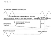
- Fig. 2 shows a diagram illustrating a transition of a voltage between both ends (hereinafter, referred to as a bus voltage Vdc) of a smoothing capacitor 31 until power is recovered from an instantaneous power failure, and a suppressing operation of a rush current in the power converter according to Embodiment 1 of the invention.
- a bus voltage Vdc a bus voltage between both ends
- the control device 20 allows the DC load control unit 23 to stop an operation of the DC load 30 when it is determined that the bus voltage Vdc detected by the DC voltage detecting unit 24 is equal to or less than a predetermined reference voltage.
- a timing at which the control device 20 allows the switching control unit 22 to turn off the switching unit 12 may be a case where the bus voltage Vdc is equal to or less than the reference voltage, or the switching unit 12 may be turned off under another condition.
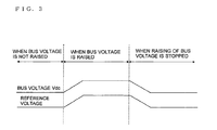
- Fig. 3 shows a diagram illustrating a relationship between the bus voltage Vdc and the reference voltage in the power converter according to Embodiment 1 of the invention.
- the method of setting the reference voltage described above will be described with reference to Fig. 3 .
- the active converter 40 operates as an ordinary passive diode bridge as described above and rectifies the AC voltage supplied from the AC power source 10.
- the bus voltage Vdc that is a DC voltage rectified by the active converter 40 is detected by the DC voltage detecting unit 24, and the control device 20 subtracts a margin from the detected bus voltage Vdc in consideration of a false detection due to a variation in the DC load 30 or a variation in the output voltage from the active converter 40, which is caused by a voltage ripple or the like, and sets the reference voltage based on a value obtained by estimating the AC voltage of the AC power source 10, which is input to the active converter 40 from the bus voltage Vdc, in such a manner that the difference ⁇ Vin does not exceed the threshold limit value ⁇ Vrush.
- the control device 20 divides the bus voltage Vdc detected by the DC voltage detecting unit 24 by the square root of 2, and thereby the AC voltage of the AC power source 10 is estimated.
- the control device 20 determines the estimated AC voltage as the AC voltage of the AC power source 10 at the time of power recovery from the instantaneous voltage.
- the control device 20 performs the setting operation of the reference voltage as described above for each predetermined time in a period where the active converter 40 does not perform the voltage-raising operation, it is possible to handle the variation in the AC voltage (primary voltage) output from the AC power source 10, and it is possible to set a reference voltage corresponding to the varied AC voltage.
- control device 20 may include means for detecting the AC voltage of the AC power source 10 and may use the detected AC voltage instead of estimating the AC voltage of the AC power source 10 based on the bus voltage Vdc detected by the DC voltage detecting unit 24.
- the active converter 40 performs the voltage-raising operation, and in a case where an output DC voltage is raised, the raised DC voltage is detected by the DC voltage detecting unit 24 as the bus voltage Vdc, and the control device 20 subtracts a margin from the detected bus voltage Vdc in consideration of a false detection due to a variation in the DC load 30 or a variation in the output voltage from the active converter 40, which is caused by a voltage ripple or the like" and sets a reference voltage. That is, as shown in Fig. 3 , whenever the output voltage (bus voltage Vdc) of the active converter 40 is varied by the active converter control unit 21, the reference voltage is also varied in conjunction with this variation.
- the control device 20 may subtract a margin from the arbitrary DC voltage in consideration of a false detection due to a variation in the DC load 30 or a variation in the output voltage from the active converter 40, which is caused by a voltage ripple or the like, and may set a reference voltage.
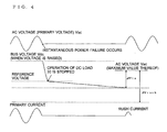
- Fig. 4 shows a diagram illustrating a transition of the bus voltage Vdc from the instantaneous power failure to recovery, and the suppressing operation of the rush current in a case where the active converter 40 of the power converter according to Embodiment 1 of the invention performs a voltage-raising operation.
- the active converter 40 performs the voltage-raising operation, as a voltage-raising level becomes large, a difference ⁇ Vin between a maximum value of an AC voltage input to the active converter 40 at the time of power recovery from the instantaneous power failure and a bus voltage Vdc immediately before the power recovery from the instantaneous power failure becomes small, and therefore it is possible to effectively suppress the rush current.
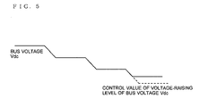
- Fig. 5 shows a diagram illustrating a control of lowering a voltage-raising level in a stepwise manner in a case where the active converter 40 of the power converter according to Embodiment 1 of the invention stops the voltage-raising operation.
- description will be given with respect to an operation where a voltage-raising level is lowered in a stepwise manner in a case where the voltage-raising operation of the active converter 40 is stopped, with reference to Fig. 5 .
- the control device 20 allows the active converter control unit 21 to perform an operation of lowering a voltage-raising level by the active converter 40 in a stepwise manner as shown in Fig. 5 . Then, the control device 20 sets a reference voltage in each voltage-raising level by the active converter 40 according to the above-described method. At this time, the control device 20 determines whether a control value of the voltage-raising level determined by the active converter control unit 21 for the active converter 40 is less than the bus voltage Vdc detected by the DC voltage detecting unit 24. When it is determined that the control value of the voltage-raising level is less than the bus voltage Vdc, the control. device 20 estimates the AC voltage of the AC power source 10 from the bus voltage Vdc and then sets the reference voltage.
- the control device 20 suppresses the dropping of the bus voltage Vdc by stopping an operation of the DC load 30, and therefore it is possible to suppress the rush current at the time of power recovery during a period before switching into a path on which a current limiting resistor 11 is provided by turning off the switching unit 12.
- the control device 20 subtracts a margin from the detected bus voltage Vdc in consideration of a false detection due to a variation in the DC load 30 or a variation in the output voltage from the active converter 40, which is caused by a voltage ripple or the like, and sets the reference voltage in such a manner that the difference ⁇ Vin does not exceed the threshold limit value ⁇ Vrush. Therefore, even when the power is recovered during a period until the switching unit 12 is turned off from the instantaneous power failure, it is possible to suppress the rush current. In addition, by suppressing the rush current in this manner, it is possible to miniaturize the semiconductor element making up the active converter 40, and it is possible to realize the cost reduction. Particularly, in a case where the semiconductor element includes a wide band gap semiconductor that is formed of SiC, GaN, diamond, or the like, the effect of the cost reduction through the miniaturization is increased.
- the reference voltage is also varied by the control device 20 in conjunction with this variation, such that the larger a voltage-raising level, the smaller a difference ⁇ Vin between a maximum value of an AC voltage input to the active converter 40 at the time of power recovery from the instantaneous power failure and a bus voltage Vdc immediately before the power recovery from the instantaneous power failure, and therefore it is possible to effectively suppress the rush current.
- the control device 20 performs a control of lowering the voltage-raising level by the active converter 40 in a stepwise manner, and determines whether a control value of the voltage-raising level determined by the active converter control unit 21 for the active converter 40 is less than the bus voltage Vdc. Then, even when the AC voltage of the AC power source 10 that is a primary voltage is varied during a voltage-raising period by the active converter 40, the varied AC voltage is estimated, and it is possible to set the reference value based on the estimated value.
Landscapes
- Engineering & Computer Science (AREA)
- Power Engineering (AREA)
- Rectifiers (AREA)
- Dc-Dc Converters (AREA)
- Inverter Devices (AREA)
Applications Claiming Priority (1)
| Application Number | Priority Date | Filing Date | Title |
|---|---|---|---|
| JP2010243084A JP5279796B2 (ja) | 2010-10-29 | 2010-10-29 | 電力変換装置 |
Publications (3)
| Publication Number | Publication Date |
|---|---|
| EP2458721A2 true EP2458721A2 (fr) | 2012-05-30 |
| EP2458721A3 EP2458721A3 (fr) | 2013-03-20 |
| EP2458721B1 EP2458721B1 (fr) | 2016-08-31 |
Family
ID=44862287
Family Applications (1)
| Application Number | Title | Priority Date | Filing Date |
|---|---|---|---|
| EP11008135.3A Not-in-force EP2458721B1 (fr) | 2010-10-29 | 2011-10-07 | Transformateur électrique |
Country Status (5)
| Country | Link |
|---|---|
| US (1) | US8711587B2 (fr) |
| EP (1) | EP2458721B1 (fr) |
| JP (1) | JP5279796B2 (fr) |
| CN (1) | CN102570434B (fr) |
| ES (1) | ES2594341T3 (fr) |
Families Citing this family (20)
| Publication number | Priority date | Publication date | Assignee | Title |
|---|---|---|---|---|
| US20120274288A1 (en) * | 2009-09-23 | 2012-11-01 | Rudolf Wegener | Providing in rush current tolerance to an electronic device |
| JP5929457B2 (ja) * | 2012-04-17 | 2016-06-08 | 岩崎電気株式会社 | 電源回路及びそれを用いたled照明装置 |
| JP5666065B1 (ja) * | 2013-04-17 | 2015-02-12 | 三菱電機株式会社 | スイッチング電源回路およびその制御方法 |
| WO2014170976A1 (fr) | 2013-04-17 | 2014-10-23 | 三菱電機株式会社 | Circuit d'alimentation à découpage et procédé de commande associé |
| CN107245837B (zh) * | 2013-07-24 | 2019-01-08 | 松下知识产权经营株式会社 | 电设备 |
| JP6153491B2 (ja) | 2014-03-28 | 2017-06-28 | オムロンオートモーティブエレクトロニクス株式会社 | 電力供給装置 |
| US9588528B2 (en) | 2014-12-01 | 2017-03-07 | Honeywell International Inc. | Inrush current suppression circuit and method for controlling when a load may be fully energized |
| SG11201705208UA (en) * | 2015-03-11 | 2017-09-28 | Mitsubishi Electric Corp | Power supply device |
| FR3034926A1 (fr) * | 2015-04-07 | 2016-10-14 | St Microelectronics Tours Sas | Convertisseur de puissance a limitation du courant d'appel |
| FR3034924A1 (fr) | 2015-04-07 | 2016-10-14 | St Microelectronics Tours Sas | Convertisseur alternatif-continu a limitation du courant d'appel |
| JP2016200964A (ja) * | 2015-04-09 | 2016-12-01 | 株式会社ソシオネクスト | 電源回路及び半導体装置 |
| DE112015005280T5 (de) * | 2015-12-01 | 2017-09-28 | Fuji Electric Co., Ltd. | Schaltung zum verhindern eines einschaltstroms |
| JP2017164018A (ja) * | 2016-03-14 | 2017-09-21 | パナソニックIpマネジメント株式会社 | 洗濯機 |
| JPWO2017195370A1 (ja) * | 2016-05-13 | 2018-08-16 | 三菱電機株式会社 | 電力変換装置 |
| JP6245484B1 (ja) * | 2016-07-07 | 2017-12-13 | 株式会社安川電機 | モータ制御システム、初期充電装置、及び故障検出方法 |
| WO2018216144A1 (fr) * | 2017-05-24 | 2018-11-29 | 三菱電機株式会社 | Dispositif de conversion de courant |
| CN108199572B (zh) * | 2017-12-25 | 2021-03-30 | 苏州英威腾电力电子有限公司 | 一种变频器及其断电保护系统 |
| CN112154598B (zh) * | 2018-05-21 | 2024-04-16 | 三菱电机株式会社 | 功率转换装置 |
| JP7117949B2 (ja) * | 2018-09-06 | 2022-08-15 | 三菱電機株式会社 | 半導体モジュールおよび電力変換装置 |
| JP7684038B2 (ja) * | 2020-12-08 | 2025-05-27 | ニデックインスツルメンツ株式会社 | モータ駆動用電源回路の突入電流制限回路及び突入電流制限方法 |
Citations (2)
| Publication number | Priority date | Publication date | Assignee | Title |
|---|---|---|---|---|
| JPH05316640A (ja) | 1992-05-11 | 1993-11-26 | Sanyo Electric Co Ltd | 電力変換装置 |
| JPH10271668A (ja) | 1997-03-28 | 1998-10-09 | Yaskawa Electric Corp | 突入電流制限方法 |
Family Cites Families (12)
| Publication number | Priority date | Publication date | Assignee | Title |
|---|---|---|---|---|
| EP1300937B1 (fr) | 1994-07-01 | 2010-06-09 | Sharp Kabushiki Kaisha | Appareil de climatisation |
| US5920186A (en) * | 1997-05-14 | 1999-07-06 | Sony Corporation | In-rush current control circuitry |
| JPH11164555A (ja) * | 1997-11-27 | 1999-06-18 | Tdk Corp | スイッチング電源 |
| US6714429B2 (en) * | 2001-08-15 | 2004-03-30 | Astec International Limited | Active inrush current control for AC to DC converters |
| KR100541724B1 (ko) | 2002-11-08 | 2006-01-11 | 삼성전자주식회사 | 모터전원공급장치 및 모터전원공급방법 |
| JP2005137054A (ja) * | 2003-10-28 | 2005-05-26 | Nec Tokin Corp | 電源回路 |
| KR101117250B1 (ko) | 2005-08-18 | 2012-03-16 | 삼성전자주식회사 | 삼상 전력 제어 시스템 및 그 제어방법 |
| JP5008425B2 (ja) * | 2007-03-07 | 2012-08-22 | 富士通テレコムネットワークス株式会社 | 停電検出回路を備えた電源装置 |
| JP5029182B2 (ja) * | 2007-07-18 | 2012-09-19 | ソニー株式会社 | 電源装置 |
| US7911352B2 (en) * | 2007-11-19 | 2011-03-22 | Teknic, Inc. | Method and apparatus for protection of AC-DC power converters |
| JP5274236B2 (ja) | 2008-12-25 | 2013-08-28 | 株式会社日立製作所 | 3相インバータの電源回路保護装置 |
| JP2010238835A (ja) * | 2009-03-31 | 2010-10-21 | Fuji Electric Systems Co Ltd | 複合半導体整流素子とそれを用いた電力変換装置 |
-
2010
- 2010-10-29 JP JP2010243084A patent/JP5279796B2/ja not_active Expired - Fee Related
-
2011
- 2011-09-28 US US13/246,926 patent/US8711587B2/en not_active Expired - Fee Related
- 2011-10-07 ES ES11008135.3T patent/ES2594341T3/es active Active
- 2011-10-07 EP EP11008135.3A patent/EP2458721B1/fr not_active Not-in-force
- 2011-10-28 CN CN201110335200.9A patent/CN102570434B/zh not_active Expired - Fee Related
Patent Citations (2)
| Publication number | Priority date | Publication date | Assignee | Title |
|---|---|---|---|---|
| JPH05316640A (ja) | 1992-05-11 | 1993-11-26 | Sanyo Electric Co Ltd | 電力変換装置 |
| JPH10271668A (ja) | 1997-03-28 | 1998-10-09 | Yaskawa Electric Corp | 突入電流制限方法 |
Also Published As
| Publication number | Publication date |
|---|---|
| AU2011226887A1 (en) | 2012-05-17 |
| US20120106212A1 (en) | 2012-05-03 |
| CN102570434A (zh) | 2012-07-11 |
| EP2458721B1 (fr) | 2016-08-31 |
| US8711587B2 (en) | 2014-04-29 |
| EP2458721A3 (fr) | 2013-03-20 |
| ES2594341T3 (es) | 2016-12-19 |
| CN102570434B (zh) | 2014-10-22 |
| JP2012095511A (ja) | 2012-05-17 |
| JP5279796B2 (ja) | 2013-09-04 |
Similar Documents
| Publication | Publication Date | Title |
|---|---|---|
| US8711587B2 (en) | Power converter with a variable reference voltage and inrush current limiting | |
| JP5343393B2 (ja) | スイッチング電源制御用半導体装置 | |
| JP5343341B2 (ja) | スイッチング電源装置 | |
| JP5799537B2 (ja) | スイッチング電源装置の制御回路及びスイッチング電源装置 | |
| US9893546B2 (en) | Direct current power supply circuit | |
| US20130242626A1 (en) | Discharge circuits for emi filters capacitors and methods thereof | |
| US9184669B2 (en) | Power supply apparatus | |
| US9564813B2 (en) | Switching power-supply device | |
| US10128649B2 (en) | Power supply device | |
| JP5460838B2 (ja) | 電力変換装置 | |
| KR20100014787A (ko) | 전자식 동작 장치의 안전성을 증가시키기 위한 회로 어레인지먼트 및 방법 | |
| EP2843815A2 (fr) | Circuit de correction de facteur de puissance | |
| EP4113143A1 (fr) | Dispositif et procédé pour le diagnostic de défaillance d'un circuit de charge initiale d'onduleur | |
| CN102005940A (zh) | 电源装置 | |
| JP5760446B2 (ja) | 電力変換装置 | |
| EP3185257B1 (fr) | Appareil chronométreur | |
| JP2016152671A (ja) | 突入電流保護機能付電源装置 | |
| JP2015149822A (ja) | 電源装置 | |
| JP4821769B2 (ja) | コンバータ用放電回路 | |
| WO2017195370A1 (fr) | Convertisseur d'énergie électrique | |
| JP6371226B2 (ja) | 逆電流保護付きスイッチング電源装置 | |
| JPH04251571A (ja) | 突入電流防止回路 |
Legal Events
| Date | Code | Title | Description |
|---|---|---|---|
| PUAI | Public reference made under article 153(3) epc to a published international application that has entered the european phase |
Free format text: ORIGINAL CODE: 0009012 |
|
| AK | Designated contracting states |
Kind code of ref document: A2 Designated state(s): AL AT BE BG CH CY CZ DE DK EE ES FI FR GB GR HR HU IE IS IT LI LT LU LV MC MK MT NL NO PL PT RO RS SE SI SK SM TR |
|
| AX | Request for extension of the european patent |
Extension state: BA ME |
|
| PUAL | Search report despatched |
Free format text: ORIGINAL CODE: 0009013 |
|
| AK | Designated contracting states |
Kind code of ref document: A3 Designated state(s): AL AT BE BG CH CY CZ DE DK EE ES FI FR GB GR HR HU IE IS IT LI LT LU LV MC MK MT NL NO PL PT RO RS SE SI SK SM TR |
|
| AX | Request for extension of the european patent |
Extension state: BA ME |
|
| RIC1 | Information provided on ipc code assigned before grant |
Ipc: H02M 1/36 20070101AFI20130213BHEP Ipc: H02M 1/32 20070101ALI20130213BHEP |
|
| 17P | Request for examination filed |
Effective date: 20130920 |
|
| RBV | Designated contracting states (corrected) |
Designated state(s): AL AT BE BG CH CY CZ DE DK EE ES FI FR GB GR HR HU IE IS IT LI LT LU LV MC MK MT NL NO PL PT RO RS SE SI SK SM TR |
|
| GRAP | Despatch of communication of intention to grant a patent |
Free format text: ORIGINAL CODE: EPIDOSNIGR1 |
|
| INTG | Intention to grant announced |
Effective date: 20160318 |
|
| GRAS | Grant fee paid |
Free format text: ORIGINAL CODE: EPIDOSNIGR3 |
|
| GRAA | (expected) grant |
Free format text: ORIGINAL CODE: 0009210 |
|
| AK | Designated contracting states |
Kind code of ref document: B1 Designated state(s): AL AT BE BG CH CY CZ DE DK EE ES FI FR GB GR HR HU IE IS IT LI LT LU LV MC MK MT NL NO PL PT RO RS SE SI SK SM TR |
|
| REG | Reference to a national code |
Ref country code: CH Ref legal event code: EP Ref country code: GB Ref legal event code: FG4D |
|
| REG | Reference to a national code |
Ref country code: IE Ref legal event code: FG4D |
|
| REG | Reference to a national code |
Ref country code: FR Ref legal event code: PLFP Year of fee payment: 6 |
|
| REG | Reference to a national code |
Ref country code: DE Ref legal event code: R096 Ref document number: 602011029746 Country of ref document: DE |
|
| REG | Reference to a national code |
Ref country code: AT Ref legal event code: REF Ref document number: 825739 Country of ref document: AT Kind code of ref document: T Effective date: 20161015 |
|
| REG | Reference to a national code |
Ref country code: ES Ref legal event code: FG2A Ref document number: 2594341 Country of ref document: ES Kind code of ref document: T3 Effective date: 20161219 |
|
| REG | Reference to a national code |
Ref country code: LT Ref legal event code: MG4D |
|
| REG | Reference to a national code |
Ref country code: NL Ref legal event code: MP Effective date: 20160831 |
|
| REG | Reference to a national code |
Ref country code: AT Ref legal event code: MK05 Ref document number: 825739 Country of ref document: AT Kind code of ref document: T Effective date: 20160831 |
|
| PG25 | Lapsed in a contracting state [announced via postgrant information from national office to epo] |
Ref country code: HR Free format text: LAPSE BECAUSE OF FAILURE TO SUBMIT A TRANSLATION OF THE DESCRIPTION OR TO PAY THE FEE WITHIN THE PRESCRIBED TIME-LIMIT Effective date: 20160831 Ref country code: RS Free format text: LAPSE BECAUSE OF FAILURE TO SUBMIT A TRANSLATION OF THE DESCRIPTION OR TO PAY THE FEE WITHIN THE PRESCRIBED TIME-LIMIT Effective date: 20160831 Ref country code: FI Free format text: LAPSE BECAUSE OF FAILURE TO SUBMIT A TRANSLATION OF THE DESCRIPTION OR TO PAY THE FEE WITHIN THE PRESCRIBED TIME-LIMIT Effective date: 20160831 Ref country code: NO Free format text: LAPSE BECAUSE OF FAILURE TO SUBMIT A TRANSLATION OF THE DESCRIPTION OR TO PAY THE FEE WITHIN THE PRESCRIBED TIME-LIMIT Effective date: 20161130 Ref country code: LT Free format text: LAPSE BECAUSE OF FAILURE TO SUBMIT A TRANSLATION OF THE DESCRIPTION OR TO PAY THE FEE WITHIN THE PRESCRIBED TIME-LIMIT Effective date: 20160831 |
|
| PG25 | Lapsed in a contracting state [announced via postgrant information from national office to epo] |
Ref country code: BE Free format text: LAPSE BECAUSE OF NON-PAYMENT OF DUE FEES Effective date: 20161031 Ref country code: AT Free format text: LAPSE BECAUSE OF FAILURE TO SUBMIT A TRANSLATION OF THE DESCRIPTION OR TO PAY THE FEE WITHIN THE PRESCRIBED TIME-LIMIT Effective date: 20160831 Ref country code: GR Free format text: LAPSE BECAUSE OF FAILURE TO SUBMIT A TRANSLATION OF THE DESCRIPTION OR TO PAY THE FEE WITHIN THE PRESCRIBED TIME-LIMIT Effective date: 20161201 Ref country code: NL Free format text: LAPSE BECAUSE OF FAILURE TO SUBMIT A TRANSLATION OF THE DESCRIPTION OR TO PAY THE FEE WITHIN THE PRESCRIBED TIME-LIMIT Effective date: 20160831 Ref country code: LV Free format text: LAPSE BECAUSE OF FAILURE TO SUBMIT A TRANSLATION OF THE DESCRIPTION OR TO PAY THE FEE WITHIN THE PRESCRIBED TIME-LIMIT Effective date: 20160831 Ref country code: SE Free format text: LAPSE BECAUSE OF FAILURE TO SUBMIT A TRANSLATION OF THE DESCRIPTION OR TO PAY THE FEE WITHIN THE PRESCRIBED TIME-LIMIT Effective date: 20160831 |
|
| PG25 | Lapsed in a contracting state [announced via postgrant information from national office to epo] |
Ref country code: RO Free format text: LAPSE BECAUSE OF FAILURE TO SUBMIT A TRANSLATION OF THE DESCRIPTION OR TO PAY THE FEE WITHIN THE PRESCRIBED TIME-LIMIT Effective date: 20160831 Ref country code: EE Free format text: LAPSE BECAUSE OF FAILURE TO SUBMIT A TRANSLATION OF THE DESCRIPTION OR TO PAY THE FEE WITHIN THE PRESCRIBED TIME-LIMIT Effective date: 20160831 |
|
| PG25 | Lapsed in a contracting state [announced via postgrant information from national office to epo] |
Ref country code: CZ Free format text: LAPSE BECAUSE OF FAILURE TO SUBMIT A TRANSLATION OF THE DESCRIPTION OR TO PAY THE FEE WITHIN THE PRESCRIBED TIME-LIMIT Effective date: 20160831 Ref country code: PT Free format text: LAPSE BECAUSE OF FAILURE TO SUBMIT A TRANSLATION OF THE DESCRIPTION OR TO PAY THE FEE WITHIN THE PRESCRIBED TIME-LIMIT Effective date: 20170102 Ref country code: SK Free format text: LAPSE BECAUSE OF FAILURE TO SUBMIT A TRANSLATION OF THE DESCRIPTION OR TO PAY THE FEE WITHIN THE PRESCRIBED TIME-LIMIT Effective date: 20160831 Ref country code: SM Free format text: LAPSE BECAUSE OF FAILURE TO SUBMIT A TRANSLATION OF THE DESCRIPTION OR TO PAY THE FEE WITHIN THE PRESCRIBED TIME-LIMIT Effective date: 20160831 Ref country code: PL Free format text: LAPSE BECAUSE OF FAILURE TO SUBMIT A TRANSLATION OF THE DESCRIPTION OR TO PAY THE FEE WITHIN THE PRESCRIBED TIME-LIMIT Effective date: 20160831 Ref country code: BE Free format text: LAPSE BECAUSE OF FAILURE TO SUBMIT A TRANSLATION OF THE DESCRIPTION OR TO PAY THE FEE WITHIN THE PRESCRIBED TIME-LIMIT Effective date: 20160831 Ref country code: DK Free format text: LAPSE BECAUSE OF FAILURE TO SUBMIT A TRANSLATION OF THE DESCRIPTION OR TO PAY THE FEE WITHIN THE PRESCRIBED TIME-LIMIT Effective date: 20160831 Ref country code: BG Free format text: LAPSE BECAUSE OF FAILURE TO SUBMIT A TRANSLATION OF THE DESCRIPTION OR TO PAY THE FEE WITHIN THE PRESCRIBED TIME-LIMIT Effective date: 20161130 |
|
| REG | Reference to a national code |
Ref country code: CH Ref legal event code: PL |
|
| REG | Reference to a national code |
Ref country code: DE Ref legal event code: R097 Ref document number: 602011029746 Country of ref document: DE |
|
| PG25 | Lapsed in a contracting state [announced via postgrant information from national office to epo] |
Ref country code: IT Free format text: LAPSE BECAUSE OF FAILURE TO SUBMIT A TRANSLATION OF THE DESCRIPTION OR TO PAY THE FEE WITHIN THE PRESCRIBED TIME-LIMIT Effective date: 20160831 |
|
| PLBE | No opposition filed within time limit |
Free format text: ORIGINAL CODE: 0009261 |
|
| STAA | Information on the status of an ep patent application or granted ep patent |
Free format text: STATUS: NO OPPOSITION FILED WITHIN TIME LIMIT |
|
| REG | Reference to a national code |
Ref country code: IE Ref legal event code: MM4A |
|
| PG25 | Lapsed in a contracting state [announced via postgrant information from national office to epo] |
Ref country code: CH Free format text: LAPSE BECAUSE OF NON-PAYMENT OF DUE FEES Effective date: 20161031 Ref country code: LI Free format text: LAPSE BECAUSE OF NON-PAYMENT OF DUE FEES Effective date: 20161031 |
|
| 26N | No opposition filed |
Effective date: 20170601 |
|
| PG25 | Lapsed in a contracting state [announced via postgrant information from national office to epo] |
Ref country code: LU Free format text: LAPSE BECAUSE OF NON-PAYMENT OF DUE FEES Effective date: 20161007 Ref country code: SI Free format text: LAPSE BECAUSE OF FAILURE TO SUBMIT A TRANSLATION OF THE DESCRIPTION OR TO PAY THE FEE WITHIN THE PRESCRIBED TIME-LIMIT Effective date: 20160831 |
|
| REG | Reference to a national code |
Ref country code: FR Ref legal event code: PLFP Year of fee payment: 7 |
|
| PG25 | Lapsed in a contracting state [announced via postgrant information from national office to epo] |
Ref country code: IE Free format text: LAPSE BECAUSE OF NON-PAYMENT OF DUE FEES Effective date: 20161007 |
|
| PG25 | Lapsed in a contracting state [announced via postgrant information from national office to epo] |
Ref country code: CY Free format text: LAPSE BECAUSE OF FAILURE TO SUBMIT A TRANSLATION OF THE DESCRIPTION OR TO PAY THE FEE WITHIN THE PRESCRIBED TIME-LIMIT Effective date: 20160831 Ref country code: HU Free format text: LAPSE BECAUSE OF FAILURE TO SUBMIT A TRANSLATION OF THE DESCRIPTION OR TO PAY THE FEE WITHIN THE PRESCRIBED TIME-LIMIT; INVALID AB INITIO Effective date: 20111007 |
|
| PG25 | Lapsed in a contracting state [announced via postgrant information from national office to epo] |
Ref country code: TR Free format text: LAPSE BECAUSE OF FAILURE TO SUBMIT A TRANSLATION OF THE DESCRIPTION OR TO PAY THE FEE WITHIN THE PRESCRIBED TIME-LIMIT Effective date: 20160831 Ref country code: MC Free format text: LAPSE BECAUSE OF FAILURE TO SUBMIT A TRANSLATION OF THE DESCRIPTION OR TO PAY THE FEE WITHIN THE PRESCRIBED TIME-LIMIT Effective date: 20160831 Ref country code: IS Free format text: LAPSE BECAUSE OF FAILURE TO SUBMIT A TRANSLATION OF THE DESCRIPTION OR TO PAY THE FEE WITHIN THE PRESCRIBED TIME-LIMIT Effective date: 20160831 Ref country code: MK Free format text: LAPSE BECAUSE OF FAILURE TO SUBMIT A TRANSLATION OF THE DESCRIPTION OR TO PAY THE FEE WITHIN THE PRESCRIBED TIME-LIMIT Effective date: 20160831 Ref country code: MT Free format text: LAPSE BECAUSE OF NON-PAYMENT OF DUE FEES Effective date: 20161031 |
|
| REG | Reference to a national code |
Ref country code: FR Ref legal event code: PLFP Year of fee payment: 8 |
|
| PG25 | Lapsed in a contracting state [announced via postgrant information from national office to epo] |
Ref country code: AL Free format text: LAPSE BECAUSE OF FAILURE TO SUBMIT A TRANSLATION OF THE DESCRIPTION OR TO PAY THE FEE WITHIN THE PRESCRIBED TIME-LIMIT Effective date: 20160831 |
|
| REG | Reference to a national code |
Ref country code: DE Ref legal event code: R084 Ref document number: 602011029746 Country of ref document: DE |
|
| REG | Reference to a national code |
Ref country code: GB Ref legal event code: 746 Effective date: 20190123 |
|
| REG | Reference to a national code |
Ref country code: ES Ref legal event code: GC2A Effective date: 20190422 |
|
| PGFP | Annual fee paid to national office [announced via postgrant information from national office to epo] |
Ref country code: FR Payment date: 20200914 Year of fee payment: 10 Ref country code: GB Payment date: 20200930 Year of fee payment: 10 |
|
| PGFP | Annual fee paid to national office [announced via postgrant information from national office to epo] |
Ref country code: DE Payment date: 20200922 Year of fee payment: 10 Ref country code: ES Payment date: 20201104 Year of fee payment: 10 |
|
| REG | Reference to a national code |
Ref country code: DE Ref legal event code: R119 Ref document number: 602011029746 Country of ref document: DE |
|
| GBPC | Gb: european patent ceased through non-payment of renewal fee |
Effective date: 20211007 |
|
| PG25 | Lapsed in a contracting state [announced via postgrant information from national office to epo] |
Ref country code: GB Free format text: LAPSE BECAUSE OF NON-PAYMENT OF DUE FEES Effective date: 20211007 Ref country code: DE Free format text: LAPSE BECAUSE OF NON-PAYMENT OF DUE FEES Effective date: 20220503 |
|
| PG25 | Lapsed in a contracting state [announced via postgrant information from national office to epo] |
Ref country code: FR Free format text: LAPSE BECAUSE OF NON-PAYMENT OF DUE FEES Effective date: 20211031 |
|
| REG | Reference to a national code |
Ref country code: ES Ref legal event code: FD2A Effective date: 20230214 |
|
| PG25 | Lapsed in a contracting state [announced via postgrant information from national office to epo] |
Ref country code: ES Free format text: LAPSE BECAUSE OF NON-PAYMENT OF DUE FEES Effective date: 20211008 |