EP2460196B1 - Thermoelektrische vorrichtung mit halbleitertechnologie - Google Patents
Thermoelektrische vorrichtung mit halbleitertechnologie Download PDFInfo
- Publication number
- EP2460196B1 EP2460196B1 EP10737880.4A EP10737880A EP2460196B1 EP 2460196 B1 EP2460196 B1 EP 2460196B1 EP 10737880 A EP10737880 A EP 10737880A EP 2460196 B1 EP2460196 B1 EP 2460196B1
- Authority
- EP
- European Patent Office
- Prior art keywords
- temperature
- sensor
- thermoelectric device
- heat source
- hot
- Prior art date
- Legal status (The legal status is an assumption and is not a legal conclusion. Google has not performed a legal analysis and makes no representation as to the accuracy of the status listed.)
- Not-in-force
Links
- 238000005516 engineering process Methods 0.000 title claims description 16
- 239000004065 semiconductor Substances 0.000 title claims description 5
- 239000002184 metal Substances 0.000 claims description 15
- 229910052751 metal Inorganic materials 0.000 claims description 15
- 238000010438 heat treatment Methods 0.000 claims description 7
- 239000012212 insulator Substances 0.000 claims description 6
- 238000001816 cooling Methods 0.000 claims description 2
- 238000001465 metallisation Methods 0.000 description 10
- 230000007423 decrease Effects 0.000 description 7
- 239000000758 substrate Substances 0.000 description 6
- 230000001052 transient effect Effects 0.000 description 6
- 230000008033 biological extinction Effects 0.000 description 5
- 229910021420 polycrystalline silicon Inorganic materials 0.000 description 5
- 230000004044 response Effects 0.000 description 5
- 230000005678 Seebeck effect Effects 0.000 description 4
- 230000008901 benefit Effects 0.000 description 4
- 230000008859 change Effects 0.000 description 4
- 230000001965 increasing effect Effects 0.000 description 4
- 238000009413 insulation Methods 0.000 description 4
- 238000005259 measurement Methods 0.000 description 4
- XUIMIQQOPSSXEZ-UHFFFAOYSA-N Silicon Chemical compound [Si] XUIMIQQOPSSXEZ-UHFFFAOYSA-N 0.000 description 3
- 230000035945 sensitivity Effects 0.000 description 3
- 229910052710 silicon Inorganic materials 0.000 description 3
- 239000010703 silicon Substances 0.000 description 3
- 230000009471 action Effects 0.000 description 2
- 238000012512 characterization method Methods 0.000 description 2
- 230000002349 favourable effect Effects 0.000 description 2
- 230000010354 integration Effects 0.000 description 2
- 230000002093 peripheral effect Effects 0.000 description 2
- 241001415961 Gaviidae Species 0.000 description 1
- 238000009825 accumulation Methods 0.000 description 1
- 238000013459 approach Methods 0.000 description 1
- 230000000903 blocking effect Effects 0.000 description 1
- 238000004364 calculation method Methods 0.000 description 1
- 239000000470 constituent Substances 0.000 description 1
- 238000010276 construction Methods 0.000 description 1
- 230000000694 effects Effects 0.000 description 1
- 238000010292 electrical insulation Methods 0.000 description 1
- 230000000763 evoking effect Effects 0.000 description 1
- 238000013213 extrapolation Methods 0.000 description 1
- 238000002513 implantation Methods 0.000 description 1
- 239000000463 material Substances 0.000 description 1
- 150000004767 nitrides Chemical class 0.000 description 1
- 238000005457 optimization Methods 0.000 description 1
- 230000000737 periodic effect Effects 0.000 description 1
- 238000005498 polishing Methods 0.000 description 1
- 230000001737 promoting effect Effects 0.000 description 1
- 230000009467 reduction Effects 0.000 description 1
- 239000000126 substance Substances 0.000 description 1
- 230000002123 temporal effect Effects 0.000 description 1
Images


Classifications
-
- G—PHYSICS
- G01—MEASURING; TESTING
- G01K—MEASURING TEMPERATURE; MEASURING QUANTITY OF HEAT; THERMALLY-SENSITIVE ELEMENTS NOT OTHERWISE PROVIDED FOR
- G01K7/00—Measuring temperature based on the use of electric or magnetic elements directly sensitive to heat ; Power supply therefor, e.g. using thermoelectric elements
- G01K7/02—Measuring temperature based on the use of electric or magnetic elements directly sensitive to heat ; Power supply therefor, e.g. using thermoelectric elements using thermoelectric elements, e.g. thermocouples
- G01K7/028—Measuring temperature based on the use of electric or magnetic elements directly sensitive to heat ; Power supply therefor, e.g. using thermoelectric elements using thermoelectric elements, e.g. thermocouples using microstructures, e.g. made of silicon
-
- H—ELECTRICITY
- H10—SEMICONDUCTOR DEVICES; ELECTRIC SOLID-STATE DEVICES NOT OTHERWISE PROVIDED FOR
- H10N—ELECTRIC SOLID-STATE DEVICES NOT OTHERWISE PROVIDED FOR
- H10N10/00—Thermoelectric devices comprising a junction of dissimilar materials, i.e. devices exhibiting Seebeck or Peltier effects
- H10N10/10—Thermoelectric devices comprising a junction of dissimilar materials, i.e. devices exhibiting Seebeck or Peltier effects operating with only the Peltier or Seebeck effects
-
- H—ELECTRICITY
- H10—SEMICONDUCTOR DEVICES; ELECTRIC SOLID-STATE DEVICES NOT OTHERWISE PROVIDED FOR
- H10N—ELECTRIC SOLID-STATE DEVICES NOT OTHERWISE PROVIDED FOR
- H10N10/00—Thermoelectric devices comprising a junction of dissimilar materials, i.e. devices exhibiting Seebeck or Peltier effects
- H10N10/10—Thermoelectric devices comprising a junction of dissimilar materials, i.e. devices exhibiting Seebeck or Peltier effects operating with only the Peltier or Seebeck effects
- H10N10/17—Thermoelectric devices comprising a junction of dissimilar materials, i.e. devices exhibiting Seebeck or Peltier effects operating with only the Peltier or Seebeck effects characterised by the structure or configuration of the cell or thermocouple forming the device
-
- H—ELECTRICITY
- H10—SEMICONDUCTOR DEVICES; ELECTRIC SOLID-STATE DEVICES NOT OTHERWISE PROVIDED FOR
- H10N—ELECTRIC SOLID-STATE DEVICES NOT OTHERWISE PROVIDED FOR
- H10N19/00—Integrated devices, or assemblies of multiple devices, comprising at least one thermoelectric or thermomagnetic element covered by groups H10N10/00 - H10N15/00
-
- G—PHYSICS
- G01—MEASURING; TESTING
- G01J—MEASUREMENT OF INTENSITY, VELOCITY, SPECTRAL CONTENT, POLARISATION, PHASE OR PULSE CHARACTERISTICS OF INFRARED, VISIBLE OR ULTRAVIOLET LIGHT; COLORIMETRY; RADIATION PYROMETRY
- G01J5/00—Radiation pyrometry, e.g. infrared or optical thermometry
- G01J5/10—Radiation pyrometry, e.g. infrared or optical thermometry using electric radiation detectors
- G01J5/12—Radiation pyrometry, e.g. infrared or optical thermometry using electric radiation detectors using thermoelectric elements, e.g. thermocouples
Definitions
- thermoelectric device in particular Seebeck effect, integrated in semiconductor technology.
- a power management circuit will cause, for example, the shutdown of a function, the slowing of a clock, or the triggering of a fan, when the temperature of the sensor reaches a threshold.
- Thermal sensors used today in integrated circuits are generally in the form of a live-polarized p-n junction.
- the voltage across the diode is indicative of the temperature of the junction.
- Such sensors have the disadvantage of consuming a permanent current, of the order of 20 ⁇ A, and especially of being not very precise on the threshold temperature (estimated at +/- 20 ° C). Although commonly used today in mobile devices, the limits of use of these sensors begin to appear because of the ever increasing power dissipation in the housings, related to the introduction of faster or new functions.
- thermal sensors There are more accurate autonomous sensors without power consumption, called Seebeck effect sensors. They are also known as “thermocouples”. These thermal sensors are differential and require the simultaneous availability of a cold source and a hot source.
- the figure 1 represents a Seebeck effect differential sensor integrated in CMOS technology, as described in the article entitled “Differential Temperature Sensors in 0.35 ⁇ m CMOS Technology", published at Therminic 2005 conference by Eduardo Aldrete-Vidrio, Diego Mateo, and Josep Altet .
- thermocouples are thus formed at the metallizations 10, arranged in series in order to increase the sensitivity of the sensor. This arrangement is also called "thermopile".
- the voltage U across the sensor, supplied to a measuring circuit 15, is proportional to the temperature difference between the thermocouples located on the hot source side and the thermocouples located on the cold source side (to simplify below one will talk about hot and cold sides of the sensor).
- the coefficient of proportionality is itself proportional to the number of thermocouples and the Seebeck coefficient of the pair of materials used for the bars.
- the figure 2 represents an example of transient temperature evolution of the hot side Th of a thermopile in response to an ideal power level P dissipated by the hot source.
- the temperature Th gradually increases and tends asymptotically towards the temperature value corresponding to the thermodynamic equilibrium.
- the growth rate depends on the power and heat capacity of the hot source.
- the maximum value depends on the power and the ability to remove heat from the hot source.
- the voltage across the sensor is directly indicative of the temperature variations of the hot source Th.
- thermal sensor that is both accurate, low consumption, and adapted by its dimensions for use in commercial integrated circuits.
- thermoelectric device integrated in semiconductor technology comprising a hot side arranged near a heat source, and a cold side, providing a signal depending on the temperature difference between hot and cold sides.
- the hot and cold sides are arranged so that their temperatures tend to equalize when the temperature of the heat source varies, i.e., the sensor is in poor operating conditions.
- a measurement circuit generates useful information according to a continuously variable portion of the signal from a time when the temperature of the heat source varies. If the temperature of the heat source ceases to vary, the temperatures of the hot and cold sides eventually equalize and the signal vanishes and ceases to vary.
- the distance between the hot and cold sides can be less than 100 ⁇ m .
- the width of the sensor can be dictated by the size of the technology and the number of junctions to achieve the desired sensitivity, there is no latitude on the length of the sensor. In current technologies, it is desired that this length be less than 100 ⁇ m , preferably less than 50 ⁇ m , that is to say five to ten times smaller than the length of the conventional sensor described in relation to the figure 1 .
- the figure 3 represents an example of temperature and voltage evolution U at the terminals of a Seebeck effect-type thermal sensor of the figure 1 , in response to a power step P applied to the hot source, in a unfavorable situation (non-thermostatic cold side Th). Such a situation is all the more unfavorable as the length of the sensor is reduced.
- the temperature Th on the warm side changes as figure 2 .
- the heat generated at the hot source is transmitted by conduction to the cold source, whose temperature Tc begins to grow from a time t1, with a certain delay depending on the length of the sensor and the thermal characteristics of the heat sink. matter between hot and cold springs.
- the growth of the temperature Tc is slower than that of the temperature Th, because the heat of the hot source is diffused all around this source, and only a fraction is diffused towards the cold source.
- the temperature Tc asymptotically tends towards the thermodynamic equilibrium temperature, which depends on the heat sink capacity of the cold source and which, in the worst case represented, is equal to the maximum value of Th.
- the voltage U at the terminals of the sensor follows the evolution of the temperature Th. From time t1, when the temperature Tc begins to increase, the voltage U starts to decrease towards 0 at as the temperature Tc approaches the temperature Th. With a sensor length of the order of 50 ⁇ m integrated in the current technologies, the duration of this pulse of the voltage U is of the order of a few microseconds. Thus the sensor becomes unusable after a few microseconds to perform the measurements mentioned in the state of the art.
- a reduced-size differential sensor usable, its hot side is placed in the immediate vicinity of a power transistor responsible for a warm-up, or which one wants to measure the heating.
- the cold side is placed away from the transistor, preferably in a zone which is not affected by another power transistor and if possible close to a ground connection connected to the conductive ground plane of the circuit to benefit from a greater thermal inertia. Then, instead of measuring a continuous temperature differential in steady state, the transient amplitude of the temperature differential is measured.
- the figure 4a represents an example of evolution of the temperatures on the hot side Th and the cold side Tc, and the corresponding voltage U across the sensor terminals, in the case where the conduction phase of the hash is substantially equal to the time set by the temperatures Tc and Th to join after turning on the transistor.
- the transistor is turned on, which corresponds to the application of a power step P.
- the temperatures Th and Tc, and the voltage U evolve as in FIG. figure 3 , starting from an equilibrium temperature T0 corresponding to the average temperature of the zone.
- the time t1 is identifiable on the signal U in that the signal U reaches its peak value.
- the pulses of the voltage U will have substantially the same amplitude and pace, but they will be more spaced.
- the voltage U proportional to the difference of the temperatures Th and Tc, presents a symmetrical alternative appearance. It can be seen that the peak values of the signal are lower than those of the figure 4a . Peak values decrease when the hash frequency increases from the situation of the figure 4a , which shows the maximum limit of hash frequency that the sensor is likely to observe given its dimensions and the thermal inertia of the system.
- the transistors that one wishes to observe operate rather under the conditions of the figure 4a , or at a lower hash frequency.
- the figure 4c represents a situation where the duty cycle of the hash is close to 1.
- the conduction phases of the transistor correspond to those of the figure 4a that is, they are long enough for the temperatures Th and Tc to reach their maximum value.
- the phases of extinction of the transistor are close to the delay of the evolution of the cold side temperature Tc.
- the voltage U evolves asymmetrically. It is representative of the temperature Th only during the extinction phases, where the voltage U has negative maximum peak values.
- a differential thermal sensor as described herein does not lend itself to a direct determination of the absolute thermal conditions of a transistor. However, in many potential applications of power management, knowing the temperature variations is sufficient to infer trends and take the desired action to change these trends. For example, it is possible to detect a condition requiring a power reduction because the voltage U supplied by the sensor increases faster than during previous conduction phases of the transistor, or the variation of the voltage U in a conduction phase. exceeds a threshold.
- a measurement circuit using the signal U will be designed by the skilled person according to his needs. It can be associated with a calculator if we want to extrapolate trends.
- An existing microcontroller to manage other functions of the integrated circuit, for example energy management, can be programmed to perform the necessary calculations, and perform the desired actions.
- the integrated circuit is made on a P-type silicon substrate (PWell).
- the MOS transistor, type N is of conventional construction. It comprises a channel 16 covered with a polycrystalline silicon gate 18. The channel is delimited by N + zones 20 and 22. The N + zone 22 can be connected to the channel by an "extension" zone N- of smaller thickness as shown.
- Contacts 24 and 26, made in a first interconnection level M1 are connected via vias to the N + zones 20 and 22, and constitute the source and drain electrodes of the transistor.
- Zone P under channel 16 is configured as an isolated box (PWell Iso).
- This box P is delimited by a buried N box (DNW), and a peripheral N box (NWell).
- Contacts 28, 30, and 32, made in the interconnection level M1 make it possible to make contact with the PWell substrate, the NWell peripheral box, and the isolated P box (PWell Iso) via respective zones P +, N + and P +.
- These various areas are insulated from each other by shallow trench insulation (commonly called STI, meaning "shallow trench insulator").
- the sensor to the left of the axis A, comprises a thermopile as described in connection with the figure 1 .
- the polycrystalline silicon bars 12 and 14 of the sensor are arranged on a shallow trench insulator 34, made in the substrate. This electrical insulation proves to be also a thermal insulator limiting the heat transfer between the substrate and the sensor, as well as between the hot and cold sides of the sensor.
- Other insulators, such as thick oxide or nitride, can be envisaged.
- the cold side of the sensor is preferably connected by a thermal bridge, formed by a stack of vias and metallizations in the successive interconnection levels (only two are represented, M1 and M2) , to a metal pad (not shown) on the surface of the chip.
- This range may be connected to a heat dissipating element via a contact ball.
- the objective is to thermally connect the cold side of the sensor ideally to a thermostat to maintain it at a temperature Tc as constant as possible.
- a contact ball connected to the ground plane of the circuit may have good thermal inertia with respect to the time required for the measurement on the sensor. This thermal inertia can be increased also by realizing thermal brakes in the ground plane to separate the power ground plugs from control ground sockets as can be realized by those skilled in the art.
- the vias which are made in large numbers to reduce the thermal resistance, do not make electrical contact with the bars 12 and 14. They come on the insulator 34 around the ends of the bars to capture the heat. Only dedicated vias connect the output contacts of the sensor to metal tracks for transmitting the voltage U supplied by the sensor to an operating circuit.
- the zone where the transistor heats up is the channel 16.
- the hot side of the sensor must be placed closer to the channel. But, as shown, this hot side of the sensor can at best be placed in contact with the periphery of the transistor.
- the sensor must not interfere with the constituent elements of the transistor which, in the case of a power MOS transistor, as shown, place the channel relatively far from the periphery.
- a thermal bridge 36 is preferably provided in the form of metallization in the interconnection level M2, for example. This bridge is connected at one end to the source electrode 24 of the transistor and, at the other end, to the warm side of the sensor.
- the connection is via vias and, where appropriate, metallizations of the intermediate interconnection levels (M1 on the sensor side).
- the vias of the bridge thermal 36 come into contact with the STI insulation 34 around the ends of the bars 12 and 14.
- the thermal bridge 36 has an optimal efficiency, its width (non-visible dimension, perpendicular to the plane of the figure) is chosen equal, on the sensor side, to the width of the thermopile, and, on the transistor side, to the width of the source electrode 24.
- the bridge 36 forming a relatively large metal mass, and therefore a large electrical capacitance, it should be connected, transistor side, to a contact that undergoes little change in voltage.
- This is generally the source of the power transistor, which is connected to a supply potential (the ground for the N-type transistors, and the supply voltage for the P-type transistors).
- the amount of metal in each interconnection level must respect a minimum proportion of the insulation filling the gap between the metallizations, in order to obtain suitable surface states and homogeneous thicknesses after planarization operations.
- this proportion is of the order of 10 to 15%.
- This constraint is integrated in the design tools of integrated circuits, so that these tools will automatically add small metal studs (called "dummies") regularly distributed on the surface of an interconnection level when the proportion of metal is insufficient.
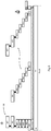
- the figure 6 represents a thermal sensor structure to optimize the length taking into account the constraints of CMP.
- a principle used in this structure is to distribute the minimum metal, in accordance with the technological needs of the CMP operation, so as to judicious, so that it disadvantages the heat transfer between the hot and cold sides of the sensor.
- the technology used as an example has seven levels of interconnection M1 to M7. In each of these levels, the minimum metal content should therefore be respected.
- a vertical stack of metallizations 38 connected by vias is provided on the cold side of the sensor, as evoked in relation to the figure 5 .
- the level metallization M1 is connected by vias to the STI insulation 34 around the ends of the bars 12, 14 of the sensor, without coming into electrical contact with them, as has been mentioned in connection with the figure 5 .
- the width of these metallizations that is to say their dimension perpendicular to the plane of the figure, is of the order of the width of the thermopile constituting the sensor.
- the level metallization M7 is preferably connected to a contact area accessible from outside the integrated circuit, which can be put directly in contact with a heat sink, or be connected by a contact ball to a metal strip of a printed circuit board.
- stepped structures 40 having metal steps in successive interconnection levels M1 to M7 are provided.
- the first staircase starts at the first level M1 at the hot end of the sensor and goes uphill towards the surface of the chip towards the cold side.
- the next staircase starts at level M1 substantially perpendicular to where the first stairway ends at level M7. With the dimensions shown, this second staircase stops at the M6 level, so as to stay away from the stack 38 on the cold side.
- this second staircase would also stop at the M7 level, and a third staircase would start at M1 level with the last step of the second staircase, and so on until it reached the stack 38.
- the steps overlap slightly from one level to the next so that they can be connected by vias.
- the first steps, level M1 do not include vias connecting them down.
- the first step of the first staircase although made in the same level M1 as the thermal bridge 36, is not connected to the thermal bridge. Indeed, these stairs are of preferably thermally and electrically isolated from the other elements of the integrated circuit.
- the depth of the steps is chosen so that the proportion of metal in each level is equal to the minimum required (10 to 15%). For example, in 65 nm CMOS technology, it will be possible to take a depth of 2.2 ⁇ m for the steps of levels M6 and M7 (where the metal is thicker), and a depth of 1.6 ⁇ m for others.
- the second staircase can start 1.2 ⁇ m after the last step of the first staircase.
- the width of the steps is of the order of the width of the thermopile constituting the sensor, as the width of the thermal bridge 36.
- Stair structures 40 act as heat deflectors, promoting upward heat propagation, away from the cold side of the sensor. Thanks to this distribution of the metal, it is possible to produce a heat-sensitive sensor with a length of the order of only 20 ⁇ m .
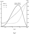
- the figure 7 represents an evolution of the temperatures hot and cold sides Th, Tc, and of the voltage U delivered by a prototype of the sensor of the type of the figure 6 in response to a power step.
- the thermopile of the sensor comprises only two polycrystalline silicon rods of types n and p, respectively, of 20 ⁇ m in length.
- the power step is such that the asymptotic value of the rise in temperature is of the order of 50 K.
- the temperature Th reaches practically this value after 100 ⁇ s .
- the cold side temperature Tc reacts with a delay of about 6 ⁇ s after the beginning of the step.
- a maximum U voltage of 4.9 mV is measured.
- this value is multiplied by 4, while having a sensor having a very small footprint. We will choose the number of bars, therefore the number of thermopile junctions, depending on the sensitivity of the circuit using the sensor output and the desired accuracy.
Landscapes
- Physics & Mathematics (AREA)
- General Physics & Mathematics (AREA)
- Chemical & Material Sciences (AREA)
- Crystallography & Structural Chemistry (AREA)
- Spectroscopy & Molecular Physics (AREA)
- Semiconductor Integrated Circuits (AREA)
- Measuring Temperature Or Quantity Of Heat (AREA)
Claims (7)
- Integrierte thermoelektrische Vorrichtung in Halbleitertechnik, umfassend eine warme Seite (Th), die in der Nähe der Wärmequelle (16) angeordnet ist, und eine kalte Seite (Tc), wobei die thermoelektrische Vorrichtung ein Signal (U), das von der Temperaturdifferenz zwischen der warmen und der kalten Seite abhängig ist, liefert, dadurch gekennzeichnet, dass:- die Wärmequelle (16) wenigstens einen MOS-Leistungstransistor umfasst, der dazu ausgelegt ist, im Zerhackermodus zu arbeiten, und der eine intermittierende Wärmequelle mit einer Heizperiode und einer Kühlperiode bildet,- der Abstand zwischen der warmen (Th) und der kalten (Tc) Seite kleiner als 100 µm ist, so dass ihre Temperaturen dazu neigen, sich auszugleichen, wenn die Temperatur der Wärmequelle (16) variiert.
- Thermoelektrische Vorrichtung nach Anspruch 1, dadurch gekennzeichnet, dass sie eine Messschaltung umfasst, die eine nützliche Information in Abhängigkeit von einem kontinuierlich variablen Abschnitt (t0-t1) des Signals ab einem Zeitpunkt, zu dem die Temperatur der Wärmequelle variiert, erstellt.
- Thermoelektrische Vorrichtung nach Anspruch 1, dadurch gekennzeichnet, dass die warme Seite mit der Wärmequelle über eine Wärmebrücke (36), welche in einer Verbindungsebene der Halbleitertechnik ausgebildet ist, verbunden ist.
- Thermoelektrische Vorrichtung nach Anspruch 1, dadurch gekennzeichnet, dass sie auf einem Isolator (34) ausgebildet ist.
- Thermoelektrische Vorrichtung nach Anspruch 1, die in einer Technik hergestellt ist, welche mehrere Verbindungsebenen (M1-M7) bietet und einen minimalen Metallanteil pro Ebene erfordert, dadurch gekennzeichnet, dass sie eine treppenförmige Struktur (40) umfasst, welche von der warmen Seite ausgeht und sich in Richtung der kalten Seite verlaufend von der Ebene des Sensors entfernt, wobei die Stufen der Struktur aus Metall in aufeinanderfolgenden Verbindungsebenen ausgebildet sind.
- Thermoelektrische Vorrichtung nach Anspruch 1, dadurch gekennzeichnet, dass sie eine Wärmebrücke (38), welche die kalte Seite mit einem von außen zugänglichen Bereich verbindet, umfasst.
- Thermoelektrische Vorrichtung nach Anspruch 3 oder 6, dadurch gekennzeichnet, dass die Wärmebrücke (36, 38) Vias umfasst, die um ein Ende der Vorrichtung herum angeordnet sind, ohne mit der Vorrichtung in elektrischen Kontakt zu gelangen.
Applications Claiming Priority (2)
| Application Number | Priority Date | Filing Date | Title |
|---|---|---|---|
| FR0903721A FR2948820A1 (fr) | 2009-07-29 | 2009-07-29 | Dispositif thermoelectrique en technologie de semi-conducteurs |
| PCT/EP2010/060820 WO2011012586A1 (fr) | 2009-07-29 | 2010-07-26 | Dispositif thermoelectrique en technologie de semi-conducteurs |
Publications (2)
| Publication Number | Publication Date |
|---|---|
| EP2460196A1 EP2460196A1 (de) | 2012-06-06 |
| EP2460196B1 true EP2460196B1 (de) | 2017-04-19 |
Family
ID=42174251
Family Applications (1)
| Application Number | Title | Priority Date | Filing Date |
|---|---|---|---|
| EP10737880.4A Not-in-force EP2460196B1 (de) | 2009-07-29 | 2010-07-26 | Thermoelektrische vorrichtung mit halbleitertechnologie |
Country Status (7)
| Country | Link |
|---|---|
| US (1) | US8829639B2 (de) |
| EP (1) | EP2460196B1 (de) |
| JP (1) | JP5738859B2 (de) |
| KR (1) | KR101742836B1 (de) |
| CN (1) | CN102598328B (de) |
| FR (1) | FR2948820A1 (de) |
| WO (1) | WO2011012586A1 (de) |
Families Citing this family (13)
| Publication number | Priority date | Publication date | Assignee | Title |
|---|---|---|---|---|
| JP5742174B2 (ja) * | 2009-12-09 | 2015-07-01 | ソニー株式会社 | 熱電発電装置、熱電発電方法及び電気信号検出方法 |
| FR2973164B1 (fr) * | 2011-03-25 | 2013-04-26 | Commissariat Energie Atomique | Capteur differentiel de temperature et ses capacites en technologie cmos/bicmos |
| FR2978871B1 (fr) * | 2011-08-02 | 2013-07-19 | Commissariat Energie Atomique | Dispositif de refroidissement muni d'un capteur thermoelectrique |
| US10777727B2 (en) * | 2011-09-08 | 2020-09-15 | Yeda Research And Development Co. Ltd. | Efficiency-enhanced thermoelectric devices |
| FR2982080B1 (fr) | 2011-10-26 | 2013-11-22 | St Microelectronics Rousset | Procede de communication sans fil entre deux dispositifs, notamment au sein d'un meme circuit integre, et systeme correspondant |
| US20130334531A1 (en) * | 2012-06-15 | 2013-12-19 | Franz Jost | Systems and methods for measuring temperature and current in integrated circuit devices |
| FR3030889B1 (fr) | 2014-12-19 | 2017-01-27 | Commissariat Energie Atomique | Capteur differentiel de temperature. |
| FR3030734B1 (fr) | 2014-12-19 | 2017-01-27 | Commissariat Energie Atomique | Capteur differentiel de temperature. |
| US9841772B2 (en) * | 2015-12-03 | 2017-12-12 | Te Connectivity Corporation | Temperature responsive thermal bridge |
| CN109037209B (zh) * | 2018-08-23 | 2024-10-29 | 格兰康希通信科技(上海)股份有限公司 | 集成电路布图结构 |
| FR3106437B1 (fr) * | 2020-01-16 | 2023-11-24 | Commissariat Energie Atomique | Composant électronique de puissance intégrant un capteur thermoélectrique |
| KR20210147562A (ko) * | 2020-05-29 | 2021-12-07 | 주식회사 테그웨이 | 열전 모듈 보호 회로 및 이를 포함하는 열전 장치 |
| CN115458671B (zh) * | 2021-06-09 | 2025-12-02 | 澜起科技股份有限公司 | 基于帕尔贴效应的集成制冷装置及其制作方法 |
Citations (1)
| Publication number | Priority date | Publication date | Assignee | Title |
|---|---|---|---|---|
| JP2002148288A (ja) * | 2000-11-08 | 2002-05-22 | Yazaki Corp | 電流検出装置 |
Family Cites Families (7)
| Publication number | Priority date | Publication date | Assignee | Title |
|---|---|---|---|---|
| JPH04335560A (ja) * | 1991-05-10 | 1992-11-24 | Hitachi Ltd | 半導体装置 |
| CN2590169Y (zh) * | 2002-12-04 | 2003-12-03 | 威盛电子股份有限公司 | 匀热式多晶片电子元件封装组件 |
| US7544883B2 (en) * | 2004-11-12 | 2009-06-09 | International Business Machines Corporation | Integrated thermoelectric cooling devices and methods for fabricating same |
| JP2006269835A (ja) * | 2005-03-24 | 2006-10-05 | Nec Electronics Corp | 半導体装置 |
| JP2007214285A (ja) * | 2006-02-08 | 2007-08-23 | Renesas Technology Corp | 半導体装置 |
| KR20080062045A (ko) * | 2006-12-29 | 2008-07-03 | 동부일렉트로닉스 주식회사 | 시모스 소자 및 그 제조 방법 |
| US8169045B2 (en) * | 2009-04-28 | 2012-05-01 | Infineon Technologies Ag | System and method for constructing shielded seebeck temperature difference sensor |
-
2009
- 2009-07-29 FR FR0903721A patent/FR2948820A1/fr active Pending
-
2010
- 2010-07-26 CN CN201080043429.9A patent/CN102598328B/zh not_active Expired - Fee Related
- 2010-07-26 WO PCT/EP2010/060820 patent/WO2011012586A1/fr not_active Ceased
- 2010-07-26 US US13/387,821 patent/US8829639B2/en not_active Expired - Fee Related
- 2010-07-26 JP JP2012522137A patent/JP5738859B2/ja not_active Expired - Fee Related
- 2010-07-26 EP EP10737880.4A patent/EP2460196B1/de not_active Not-in-force
- 2010-07-26 KR KR1020127005356A patent/KR101742836B1/ko not_active Expired - Fee Related
Patent Citations (1)
| Publication number | Priority date | Publication date | Assignee | Title |
|---|---|---|---|---|
| JP2002148288A (ja) * | 2000-11-08 | 2002-05-22 | Yazaki Corp | 電流検出装置 |
Also Published As
| Publication number | Publication date |
|---|---|
| US20120217608A1 (en) | 2012-08-30 |
| FR2948820A1 (fr) | 2011-02-04 |
| KR101742836B1 (ko) | 2017-06-01 |
| KR20120080566A (ko) | 2012-07-17 |
| CN102598328A (zh) | 2012-07-18 |
| US8829639B2 (en) | 2014-09-09 |
| WO2011012586A1 (fr) | 2011-02-03 |
| JP2013501354A (ja) | 2013-01-10 |
| JP5738859B2 (ja) | 2015-06-24 |
| CN102598328B (zh) | 2015-09-16 |
| EP2460196A1 (de) | 2012-06-06 |
Similar Documents
| Publication | Publication Date | Title |
|---|---|---|
| EP2460196B1 (de) | Thermoelektrische vorrichtung mit halbleitertechnologie | |
| US9444027B2 (en) | Thermoelectrical device and method for manufacturing same | |
| US20110128727A1 (en) | Integrated seebeck device | |
| EP2689221B1 (de) | Differenzialtemperatursensor und seine cmos/bicmos-technologiekompetenzen | |
| FR2679082A1 (fr) | Dispositif de commutation a semiconducteurs pouvant etre commande et comportant un systeme integre de limitation de courant et de coupure pour temperature excessive. | |
| FR2918926A1 (fr) | Pneumatique muni d'un dispositif thermoelectrique | |
| FR3093863A1 (fr) | Batterie et procédé de régulation thermique d’une batterie embarquée sur un véhicule électrique | |
| US9947853B2 (en) | Thermoelectric device | |
| US20250022771A1 (en) | Image sensor with actively cooled sensor array | |
| FR2977984A1 (fr) | Generateur thermoelectrique integre, et circuit integre comprenant un tel generateur | |
| FR2878077A1 (fr) | Composant electronique vertical autorefroidi | |
| Bulman et al. | High heat flux, high temperature cooling of electronics with thermoelectric devices | |
| EP0619616B1 (de) | Peltiereffektapparat zur Detektion der Wahrscheinlichkeit von Kondensationsbildung an einer Oberfläche, die sich in Kontakt mit feuchter Luft befindet | |
| FR2968134A1 (fr) | Module thermoélectrique a rendement amélioré | |
| EP3749937A1 (de) | Verfahren und vorrichtung zur erkennung einer überschreitung einer vorgegebenen temperaturschwelle | |
| FR2969826A1 (fr) | Dispositif thermoélectrique modulable et ajustable et procédé de fonctionnement du dispositif thermoélectrique | |
| FR3023415A1 (fr) | Generateur thermoelectrique a pertes reduites | |
| FR2930074A1 (fr) | Dispositif et procede d'optimisation de la generation thermoelectrique | |
| FR3144481A1 (fr) | Circuit optoelectronique comprenant des diodes electroluminescentes | |
| FR2857176A1 (fr) | Dispositif de protection pour composant electronique et circuit integre | |
| BE566689A (de) | ||
| FR3010234A1 (fr) | Controle de la plage thermique de fonctionnement d'un generateur thermoelectrique | |
| FR2950482A1 (fr) | Procede pour generer une difference de potentiel a l'aide d'une couche mince de graphene, et dispositifs faisant application |
Legal Events
| Date | Code | Title | Description |
|---|---|---|---|
| PUAI | Public reference made under article 153(3) epc to a published international application that has entered the european phase |
Free format text: ORIGINAL CODE: 0009012 |
|
| 17P | Request for examination filed |
Effective date: 20120124 |
|
| AK | Designated contracting states |
Kind code of ref document: A1 Designated state(s): AL AT BE BG CH CY CZ DE DK EE ES FI FR GB GR HR HU IE IS IT LI LT LU LV MC MK MT NL NO PL PT RO SE SI SK SM TR |
|
| DAX | Request for extension of the european patent (deleted) | ||
| 17Q | First examination report despatched |
Effective date: 20160421 |
|
| GRAP | Despatch of communication of intention to grant a patent |
Free format text: ORIGINAL CODE: EPIDOSNIGR1 |
|
| STAA | Information on the status of an ep patent application or granted ep patent |
Free format text: STATUS: GRANT OF PATENT IS INTENDED |
|
| INTG | Intention to grant announced |
Effective date: 20161222 |
|
| GRAS | Grant fee paid |
Free format text: ORIGINAL CODE: EPIDOSNIGR3 |
|
| GRAA | (expected) grant |
Free format text: ORIGINAL CODE: 0009210 |
|
| STAA | Information on the status of an ep patent application or granted ep patent |
Free format text: STATUS: THE PATENT HAS BEEN GRANTED |
|
| AK | Designated contracting states |
Kind code of ref document: B1 Designated state(s): AL AT BE BG CH CY CZ DE DK EE ES FI FR GB GR HR HU IE IS IT LI LT LU LV MC MK MT NL NO PL PT RO SE SI SK SM TR |
|
| REG | Reference to a national code |
Ref country code: GB Ref legal event code: FG4D Free format text: NOT ENGLISH |
|
| REG | Reference to a national code |
Ref country code: CH Ref legal event code: EP |
|
| REG | Reference to a national code |
Ref country code: AT Ref legal event code: REF Ref document number: 886707 Country of ref document: AT Kind code of ref document: T Effective date: 20170515 |
|
| REG | Reference to a national code |
Ref country code: IE Ref legal event code: FG4D Free format text: LANGUAGE OF EP DOCUMENT: FRENCH |
|
| REG | Reference to a national code |
Ref country code: DE Ref legal event code: R096 Ref document number: 602010041661 Country of ref document: DE |
|
| REG | Reference to a national code |
Ref country code: FR Ref legal event code: PLFP Year of fee payment: 8 |
|
| REG | Reference to a national code |
Ref country code: NL Ref legal event code: MP Effective date: 20170419 |
|
| REG | Reference to a national code |
Ref country code: LT Ref legal event code: MG4D |
|
| REG | Reference to a national code |
Ref country code: AT Ref legal event code: MK05 Ref document number: 886707 Country of ref document: AT Kind code of ref document: T Effective date: 20170419 |
|
| PG25 | Lapsed in a contracting state [announced via postgrant information from national office to epo] |
Ref country code: NL Free format text: LAPSE BECAUSE OF FAILURE TO SUBMIT A TRANSLATION OF THE DESCRIPTION OR TO PAY THE FEE WITHIN THE PRESCRIBED TIME-LIMIT Effective date: 20170419 |
|
| PG25 | Lapsed in a contracting state [announced via postgrant information from national office to epo] |
Ref country code: FI Free format text: LAPSE BECAUSE OF FAILURE TO SUBMIT A TRANSLATION OF THE DESCRIPTION OR TO PAY THE FEE WITHIN THE PRESCRIBED TIME-LIMIT Effective date: 20170419 Ref country code: GR Free format text: LAPSE BECAUSE OF FAILURE TO SUBMIT A TRANSLATION OF THE DESCRIPTION OR TO PAY THE FEE WITHIN THE PRESCRIBED TIME-LIMIT Effective date: 20170720 Ref country code: NO Free format text: LAPSE BECAUSE OF FAILURE TO SUBMIT A TRANSLATION OF THE DESCRIPTION OR TO PAY THE FEE WITHIN THE PRESCRIBED TIME-LIMIT Effective date: 20170719 Ref country code: ES Free format text: LAPSE BECAUSE OF FAILURE TO SUBMIT A TRANSLATION OF THE DESCRIPTION OR TO PAY THE FEE WITHIN THE PRESCRIBED TIME-LIMIT Effective date: 20170419 Ref country code: AT Free format text: LAPSE BECAUSE OF FAILURE TO SUBMIT A TRANSLATION OF THE DESCRIPTION OR TO PAY THE FEE WITHIN THE PRESCRIBED TIME-LIMIT Effective date: 20170419 Ref country code: LT Free format text: LAPSE BECAUSE OF FAILURE TO SUBMIT A TRANSLATION OF THE DESCRIPTION OR TO PAY THE FEE WITHIN THE PRESCRIBED TIME-LIMIT Effective date: 20170419 Ref country code: HR Free format text: LAPSE BECAUSE OF FAILURE TO SUBMIT A TRANSLATION OF THE DESCRIPTION OR TO PAY THE FEE WITHIN THE PRESCRIBED TIME-LIMIT Effective date: 20170419 |
|
| PG25 | Lapsed in a contracting state [announced via postgrant information from national office to epo] |
Ref country code: LV Free format text: LAPSE BECAUSE OF FAILURE TO SUBMIT A TRANSLATION OF THE DESCRIPTION OR TO PAY THE FEE WITHIN THE PRESCRIBED TIME-LIMIT Effective date: 20170419 Ref country code: BG Free format text: LAPSE BECAUSE OF FAILURE TO SUBMIT A TRANSLATION OF THE DESCRIPTION OR TO PAY THE FEE WITHIN THE PRESCRIBED TIME-LIMIT Effective date: 20170719 Ref country code: IS Free format text: LAPSE BECAUSE OF FAILURE TO SUBMIT A TRANSLATION OF THE DESCRIPTION OR TO PAY THE FEE WITHIN THE PRESCRIBED TIME-LIMIT Effective date: 20170819 Ref country code: SE Free format text: LAPSE BECAUSE OF FAILURE TO SUBMIT A TRANSLATION OF THE DESCRIPTION OR TO PAY THE FEE WITHIN THE PRESCRIBED TIME-LIMIT Effective date: 20170419 Ref country code: PL Free format text: LAPSE BECAUSE OF FAILURE TO SUBMIT A TRANSLATION OF THE DESCRIPTION OR TO PAY THE FEE WITHIN THE PRESCRIBED TIME-LIMIT Effective date: 20170419 |
|
| REG | Reference to a national code |
Ref country code: DE Ref legal event code: R097 Ref document number: 602010041661 Country of ref document: DE |
|
| PG25 | Lapsed in a contracting state [announced via postgrant information from national office to epo] |
Ref country code: DK Free format text: LAPSE BECAUSE OF FAILURE TO SUBMIT A TRANSLATION OF THE DESCRIPTION OR TO PAY THE FEE WITHIN THE PRESCRIBED TIME-LIMIT Effective date: 20170419 Ref country code: EE Free format text: LAPSE BECAUSE OF FAILURE TO SUBMIT A TRANSLATION OF THE DESCRIPTION OR TO PAY THE FEE WITHIN THE PRESCRIBED TIME-LIMIT Effective date: 20170419 Ref country code: SK Free format text: LAPSE BECAUSE OF FAILURE TO SUBMIT A TRANSLATION OF THE DESCRIPTION OR TO PAY THE FEE WITHIN THE PRESCRIBED TIME-LIMIT Effective date: 20170419 Ref country code: RO Free format text: LAPSE BECAUSE OF FAILURE TO SUBMIT A TRANSLATION OF THE DESCRIPTION OR TO PAY THE FEE WITHIN THE PRESCRIBED TIME-LIMIT Effective date: 20170419 Ref country code: CZ Free format text: LAPSE BECAUSE OF FAILURE TO SUBMIT A TRANSLATION OF THE DESCRIPTION OR TO PAY THE FEE WITHIN THE PRESCRIBED TIME-LIMIT Effective date: 20170419 |
|
| PLBE | No opposition filed within time limit |
Free format text: ORIGINAL CODE: 0009261 |
|
| STAA | Information on the status of an ep patent application or granted ep patent |
Free format text: STATUS: NO OPPOSITION FILED WITHIN TIME LIMIT |
|
| PG25 | Lapsed in a contracting state [announced via postgrant information from national office to epo] |
Ref country code: SM Free format text: LAPSE BECAUSE OF FAILURE TO SUBMIT A TRANSLATION OF THE DESCRIPTION OR TO PAY THE FEE WITHIN THE PRESCRIBED TIME-LIMIT Effective date: 20170419 Ref country code: IT Free format text: LAPSE BECAUSE OF FAILURE TO SUBMIT A TRANSLATION OF THE DESCRIPTION OR TO PAY THE FEE WITHIN THE PRESCRIBED TIME-LIMIT Effective date: 20170419 |
|
| REG | Reference to a national code |
Ref country code: CH Ref legal event code: PL |
|
| 26N | No opposition filed |
Effective date: 20180122 |
|
| REG | Reference to a national code |
Ref country code: IE Ref legal event code: MM4A |
|
| PG25 | Lapsed in a contracting state [announced via postgrant information from national office to epo] |
Ref country code: IE Free format text: LAPSE BECAUSE OF NON-PAYMENT OF DUE FEES Effective date: 20170726 Ref country code: CH Free format text: LAPSE BECAUSE OF NON-PAYMENT OF DUE FEES Effective date: 20170731 Ref country code: LI Free format text: LAPSE BECAUSE OF NON-PAYMENT OF DUE FEES Effective date: 20170731 |
|
| PG25 | Lapsed in a contracting state [announced via postgrant information from national office to epo] |
Ref country code: SI Free format text: LAPSE BECAUSE OF FAILURE TO SUBMIT A TRANSLATION OF THE DESCRIPTION OR TO PAY THE FEE WITHIN THE PRESCRIBED TIME-LIMIT Effective date: 20170419 |
|
| REG | Reference to a national code |
Ref country code: BE Ref legal event code: MM Effective date: 20170731 |
|
| REG | Reference to a national code |
Ref country code: FR Ref legal event code: PLFP Year of fee payment: 9 |
|
| PG25 | Lapsed in a contracting state [announced via postgrant information from national office to epo] |
Ref country code: LU Free format text: LAPSE BECAUSE OF NON-PAYMENT OF DUE FEES Effective date: 20170726 |
|
| PG25 | Lapsed in a contracting state [announced via postgrant information from national office to epo] |
Ref country code: BE Free format text: LAPSE BECAUSE OF NON-PAYMENT OF DUE FEES Effective date: 20170731 |
|
| PG25 | Lapsed in a contracting state [announced via postgrant information from national office to epo] |
Ref country code: MT Free format text: LAPSE BECAUSE OF FAILURE TO SUBMIT A TRANSLATION OF THE DESCRIPTION OR TO PAY THE FEE WITHIN THE PRESCRIBED TIME-LIMIT Effective date: 20170419 |
|
| PG25 | Lapsed in a contracting state [announced via postgrant information from national office to epo] |
Ref country code: HU Free format text: LAPSE BECAUSE OF FAILURE TO SUBMIT A TRANSLATION OF THE DESCRIPTION OR TO PAY THE FEE WITHIN THE PRESCRIBED TIME-LIMIT; INVALID AB INITIO Effective date: 20100726 Ref country code: MC Free format text: LAPSE BECAUSE OF FAILURE TO SUBMIT A TRANSLATION OF THE DESCRIPTION OR TO PAY THE FEE WITHIN THE PRESCRIBED TIME-LIMIT Effective date: 20170419 |
|
| PG25 | Lapsed in a contracting state [announced via postgrant information from national office to epo] |
Ref country code: CY Free format text: LAPSE BECAUSE OF NON-PAYMENT OF DUE FEES Effective date: 20170419 |
|
| PG25 | Lapsed in a contracting state [announced via postgrant information from national office to epo] |
Ref country code: MK Free format text: LAPSE BECAUSE OF FAILURE TO SUBMIT A TRANSLATION OF THE DESCRIPTION OR TO PAY THE FEE WITHIN THE PRESCRIBED TIME-LIMIT Effective date: 20170419 |
|
| PG25 | Lapsed in a contracting state [announced via postgrant information from national office to epo] |
Ref country code: TR Free format text: LAPSE BECAUSE OF FAILURE TO SUBMIT A TRANSLATION OF THE DESCRIPTION OR TO PAY THE FEE WITHIN THE PRESCRIBED TIME-LIMIT Effective date: 20170419 |
|
| PG25 | Lapsed in a contracting state [announced via postgrant information from national office to epo] |
Ref country code: PT Free format text: LAPSE BECAUSE OF FAILURE TO SUBMIT A TRANSLATION OF THE DESCRIPTION OR TO PAY THE FEE WITHIN THE PRESCRIBED TIME-LIMIT Effective date: 20170419 |
|
| PG25 | Lapsed in a contracting state [announced via postgrant information from national office to epo] |
Ref country code: AL Free format text: LAPSE BECAUSE OF FAILURE TO SUBMIT A TRANSLATION OF THE DESCRIPTION OR TO PAY THE FEE WITHIN THE PRESCRIBED TIME-LIMIT Effective date: 20170419 |
|
| PGFP | Annual fee paid to national office [announced via postgrant information from national office to epo] |
Ref country code: FR Payment date: 20200623 Year of fee payment: 11 |
|
| PGFP | Annual fee paid to national office [announced via postgrant information from national office to epo] |
Ref country code: GB Payment date: 20200624 Year of fee payment: 11 |
|
| PGFP | Annual fee paid to national office [announced via postgrant information from national office to epo] |
Ref country code: DE Payment date: 20200622 Year of fee payment: 11 |
|
| REG | Reference to a national code |
Ref country code: DE Ref legal event code: R119 Ref document number: 602010041661 Country of ref document: DE |
|
| GBPC | Gb: european patent ceased through non-payment of renewal fee |
Effective date: 20210726 |
|
| PG25 | Lapsed in a contracting state [announced via postgrant information from national office to epo] |
Ref country code: GB Free format text: LAPSE BECAUSE OF NON-PAYMENT OF DUE FEES Effective date: 20210726 Ref country code: DE Free format text: LAPSE BECAUSE OF NON-PAYMENT OF DUE FEES Effective date: 20220201 |
|
| PG25 | Lapsed in a contracting state [announced via postgrant information from national office to epo] |
Ref country code: FR Free format text: LAPSE BECAUSE OF NON-PAYMENT OF DUE FEES Effective date: 20210731 |