EP2461146B1 - Sensoranordnung und sensormodul - Google Patents
Sensoranordnung und sensormodul Download PDFInfo
- Publication number
- EP2461146B1 EP2461146B1 EP10818751.9A EP10818751A EP2461146B1 EP 2461146 B1 EP2461146 B1 EP 2461146B1 EP 10818751 A EP10818751 A EP 10818751A EP 2461146 B1 EP2461146 B1 EP 2461146B1
- Authority
- EP
- European Patent Office
- Prior art keywords
- sensor
- thin film
- film
- packaging bag
- sensor element
- Prior art date
- Legal status (The legal status is an assumption and is not a legal conclusion. Google has not performed a legal analysis and makes no representation as to the accuracy of the status listed.)
- Not-in-force
Links
- 239000010409 thin film Substances 0.000 claims description 174
- 239000011347 resin Substances 0.000 claims description 90
- 229920005989 resin Polymers 0.000 claims description 90
- 238000004806 packaging method and process Methods 0.000 claims description 89
- 239000010408 film Substances 0.000 claims description 71
- -1 polyethylene terephthalate Polymers 0.000 claims description 35
- 239000005001 laminate film Substances 0.000 claims description 34
- 229910052751 metal Inorganic materials 0.000 claims description 26
- 239000002184 metal Substances 0.000 claims description 26
- 239000011888 foil Substances 0.000 claims description 25
- 238000012856 packing Methods 0.000 claims description 16
- 239000004743 Polypropylene Substances 0.000 claims description 15
- 229920001155 polypropylene Polymers 0.000 claims description 15
- 229930040373 Paraformaldehyde Natural products 0.000 claims description 14
- 230000008859 change Effects 0.000 claims description 14
- 229920006324 polyoxymethylene Polymers 0.000 claims description 14
- 229920001971 elastomer Polymers 0.000 claims description 12
- 239000011112 polyethylene naphthalate Substances 0.000 claims description 12
- 239000005020 polyethylene terephthalate Substances 0.000 claims description 12
- 229920000139 polyethylene terephthalate Polymers 0.000 claims description 12
- 239000000806 elastomer Substances 0.000 claims description 11
- 239000004734 Polyphenylene sulfide Substances 0.000 claims description 9
- 229920003207 poly(ethylene-2,6-naphthalate) Polymers 0.000 claims description 9
- 229920000069 polyphenylene sulfide Polymers 0.000 claims description 9
- 239000004698 Polyethylene Substances 0.000 claims description 8
- 229920000573 polyethylene Polymers 0.000 claims description 8
- YCKRFDGAMUMZLT-UHFFFAOYSA-N Fluorine atom Chemical compound [F] YCKRFDGAMUMZLT-UHFFFAOYSA-N 0.000 claims description 7
- 239000011737 fluorine Substances 0.000 claims description 7
- 229910052731 fluorine Inorganic materials 0.000 claims description 7
- 229920000219 Ethylene vinyl alcohol Polymers 0.000 claims description 6
- 239000004952 Polyamide Substances 0.000 claims description 6
- 238000002844 melting Methods 0.000 claims description 6
- 230000008018 melting Effects 0.000 claims description 6
- 229920003229 poly(methyl methacrylate) Polymers 0.000 claims description 6
- 229920002647 polyamide Polymers 0.000 claims description 6
- 239000004926 polymethyl methacrylate Substances 0.000 claims description 6
- 239000004800 polyvinyl chloride Substances 0.000 claims description 6
- 229920000915 polyvinyl chloride Polymers 0.000 claims description 6
- 229910052782 aluminium Inorganic materials 0.000 claims description 5
- XAGFODPZIPBFFR-UHFFFAOYSA-N aluminium Chemical compound [Al] XAGFODPZIPBFFR-UHFFFAOYSA-N 0.000 claims description 5
- 239000004417 polycarbonate Substances 0.000 claims description 5
- 229920000515 polycarbonate Polymers 0.000 claims description 5
- 238000007789 sealing Methods 0.000 claims description 4
- RYGMFSIKBFXOCR-UHFFFAOYSA-N Copper Chemical compound [Cu] RYGMFSIKBFXOCR-UHFFFAOYSA-N 0.000 claims description 3
- ATJFFYVFTNAWJD-UHFFFAOYSA-N Tin Chemical compound [Sn] ATJFFYVFTNAWJD-UHFFFAOYSA-N 0.000 claims description 3
- HCHKCACWOHOZIP-UHFFFAOYSA-N Zinc Chemical compound [Zn] HCHKCACWOHOZIP-UHFFFAOYSA-N 0.000 claims description 3
- 229910052802 copper Inorganic materials 0.000 claims description 3
- 239000010949 copper Substances 0.000 claims description 3
- 229910001220 stainless steel Inorganic materials 0.000 claims description 3
- 239000010935 stainless steel Substances 0.000 claims description 3
- 229910052718 tin Inorganic materials 0.000 claims description 3
- 239000011135 tin Substances 0.000 claims description 3
- 229910052725 zinc Inorganic materials 0.000 claims description 3
- 239000011701 zinc Substances 0.000 claims description 3
- 239000000463 material Substances 0.000 description 81
- 239000010410 layer Substances 0.000 description 57
- 238000005452 bending Methods 0.000 description 48
- 239000011231 conductive filler Substances 0.000 description 35
- 239000013039 cover film Substances 0.000 description 34
- 238000009413 insulation Methods 0.000 description 32
- 239000002245 particle Substances 0.000 description 19
- 238000000034 method Methods 0.000 description 17
- 230000008569 process Effects 0.000 description 14
- 239000011248 coating agent Substances 0.000 description 11
- 238000000576 coating method Methods 0.000 description 11
- 239000011159 matrix material Substances 0.000 description 11
- 230000005489 elastic deformation Effects 0.000 description 10
- 239000000758 substrate Substances 0.000 description 10
- 229920000800 acrylic rubber Polymers 0.000 description 9
- 229920000058 polyacrylate Polymers 0.000 description 9
- 230000004044 response Effects 0.000 description 9
- QVGXLLKOCUKJST-UHFFFAOYSA-N atomic oxygen Chemical compound [O] QVGXLLKOCUKJST-UHFFFAOYSA-N 0.000 description 8
- 229910052760 oxygen Inorganic materials 0.000 description 8
- 239000001301 oxygen Substances 0.000 description 8
- 238000007650 screen-printing Methods 0.000 description 8
- BQCADISMDOOEFD-UHFFFAOYSA-N Silver Chemical compound [Ag] BQCADISMDOOEFD-UHFFFAOYSA-N 0.000 description 7
- 230000000694 effects Effects 0.000 description 7
- 238000004519 manufacturing process Methods 0.000 description 7
- 230000007423 decrease Effects 0.000 description 6
- 230000006866 deterioration Effects 0.000 description 6
- 230000035945 sensitivity Effects 0.000 description 6
- 229910052709 silver Inorganic materials 0.000 description 6
- 239000004332 silver Substances 0.000 description 6
- 239000000126 substance Substances 0.000 description 6
- OKTJSMMVPCPJKN-UHFFFAOYSA-N Carbon Chemical compound [C] OKTJSMMVPCPJKN-UHFFFAOYSA-N 0.000 description 5
- 239000011324 bead Substances 0.000 description 5
- 229910052799 carbon Inorganic materials 0.000 description 5
- 229920000840 ethylene tetrafluoroethylene copolymer Polymers 0.000 description 5
- 230000004927 fusion Effects 0.000 description 5
- 229920001343 polytetrafluoroethylene Polymers 0.000 description 5
- 239000004810 polytetrafluoroethylene Substances 0.000 description 5
- 230000002829 reductive effect Effects 0.000 description 5
- 230000000994 depressogenic effect Effects 0.000 description 4
- 238000001514 detection method Methods 0.000 description 4
- 238000005259 measurement Methods 0.000 description 4
- 238000013508 migration Methods 0.000 description 4
- 230000005012 migration Effects 0.000 description 4
- 239000013307 optical fiber Substances 0.000 description 4
- 230000035515 penetration Effects 0.000 description 4
- 229920002379 silicone rubber Polymers 0.000 description 4
- 239000004945 silicone rubber Substances 0.000 description 4
- 239000004642 Polyimide Substances 0.000 description 3
- 230000001419 dependent effect Effects 0.000 description 3
- 238000009826 distribution Methods 0.000 description 3
- 230000012447 hatching Effects 0.000 description 3
- 229920001721 polyimide Polymers 0.000 description 3
- 239000002861 polymer material Substances 0.000 description 3
- 238000002360 preparation method Methods 0.000 description 3
- 229920006311 Urethane elastomer Polymers 0.000 description 2
- 239000004676 acrylonitrile butadiene styrene Substances 0.000 description 2
- 229920000122 acrylonitrile butadiene styrene Polymers 0.000 description 2
- 230000006835 compression Effects 0.000 description 2
- 238000007906 compression Methods 0.000 description 2
- 238000005520 cutting process Methods 0.000 description 2
- 239000013536 elastomeric material Substances 0.000 description 2
- 239000003822 epoxy resin Substances 0.000 description 2
- 239000004715 ethylene vinyl alcohol Substances 0.000 description 2
- 238000009501 film coating Methods 0.000 description 2
- 230000002401 inhibitory effect Effects 0.000 description 2
- 239000011810 insulating material Substances 0.000 description 2
- 239000003273 ketjen black Substances 0.000 description 2
- 230000000670 limiting effect Effects 0.000 description 2
- 229920000647 polyepoxide Polymers 0.000 description 2
- 229920000098 polyolefin Polymers 0.000 description 2
- 238000007639 printing Methods 0.000 description 2
- 238000002604 ultrasonography Methods 0.000 description 2
- 239000004925 Acrylic resin Substances 0.000 description 1
- 229920000178 Acrylic resin Polymers 0.000 description 1
- XECAHXYUAAWDEL-UHFFFAOYSA-N acrylonitrile butadiene styrene Chemical compound C=CC=C.C=CC#N.C=CC1=CC=CC=C1 XECAHXYUAAWDEL-UHFFFAOYSA-N 0.000 description 1
- 230000003466 anti-cipated effect Effects 0.000 description 1
- 238000004891 communication Methods 0.000 description 1
- 230000003111 delayed effect Effects 0.000 description 1
- 210000001787 dendrite Anatomy 0.000 description 1
- 230000000881 depressing effect Effects 0.000 description 1
- 238000001035 drying Methods 0.000 description 1
- 150000002739 metals Chemical class 0.000 description 1
- 239000005022 packaging material Substances 0.000 description 1
- 239000011164 primary particle Substances 0.000 description 1
- 238000012545 processing Methods 0.000 description 1
- 230000009467 reduction Effects 0.000 description 1
- 239000012812 sealant material Substances 0.000 description 1
- 239000011163 secondary particle Substances 0.000 description 1
- 230000003068 static effect Effects 0.000 description 1
- 229920002725 thermoplastic elastomer Polymers 0.000 description 1
- 239000011800 void material Substances 0.000 description 1
- XLYOFNOQVPJJNP-UHFFFAOYSA-N water Substances O XLYOFNOQVPJJNP-UHFFFAOYSA-N 0.000 description 1
Images








Classifications
-
- G—PHYSICS
- G01—MEASURING; TESTING
- G01L—MEASURING FORCE, STRESS, TORQUE, WORK, MECHANICAL POWER, MECHANICAL EFFICIENCY, OR FLUID PRESSURE
- G01L1/00—Measuring force or stress, in general
- G01L1/20—Measuring force or stress, in general by measuring variations in ohmic resistance of solid materials or of electrically-conductive fluids; by making use of electrokinetic cells, i.e. liquid-containing cells wherein an electrical potential is produced or varied upon the application of stress
Definitions
- the present invention relates to a sensor assembly having a flexible sensor element that uses a polymer material. More specifically, the present invention relates to a sensor assembly having a sensor component such as a sensor element or the like that is less likely to deteriorate and is superior in durability.
- a load sensor having an elastomeric sensor thin film for example, see Patent Documents 2 and 3.
- a load sensor disclosed in Patent Document 2 a sensor thin film is formed in which conductive filler is filled in elastomer of a parent material at a predetermined state. According to this load sensor, based on a change in electrical resistance caused when the sensor thin film elastically deforms, an input load can be detected.
- a load sensor disclosed in Patent Document 3 is a capacitance-type sensor, which includes an elastomeric dielectric film and a pair of electrodes arranged sandwiching the dielectric film. According to this load sensor, based on a change in capacitance between the pair of electrodes, an input load can be detected.
- JP 5 281664 A discloses a packaging material for photographic sensitive material including a heat resistant flexible sheet, a film layer and a metallic layer disposed between the heat resistant flexible sheet and the film layer.
- a load sensor can be used in a state housed in a resin case.
- influence of moisture and oxygen with respect to a component cannot be completely eliminated.
- a sensor assembly is defined in Claim 1 and a sensor module is defined in Claim 6.
- the sensor element has the wiring unit connected to the electrical circuit.
- the wiring unit is led out from the opening of the exterior packaging bag and is connected to the electrical circuit.
- the wiring unit is housed inside the case body of the circuit case. For this reason, the wiring unit can be protected from an impact and the like.
- the packing member By using the packing member, the opening of the exterior packaging bag can be easily sealed and the sensor assembly can be installed on the circuit case.
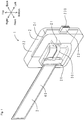
- Fig. 1 illustrates a perspective view of the sensor module according to the present embodiment.
- Fig. 2 illustrates an exploded perspective view of the sensor module.
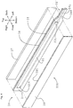
- Fig. 3 illustrates an exploded perspective view of a sensor assembly in the sensor module. In Figs. 1 - 3 , transparently visible portions are illustrated using thin lines.
- a sensor module 1 includes a circuit case 2 and a sensor assembly 3.
- the sensor module 1 is installed on a surface (front surface) of a front bumper of a vehicle (not shown in the drawings). Therefore, directions in the drawings are defined relative to a traveling direction of the vehicle.
- a load is input to the sensor assembly 3 from the front.
- the circuit case 2 includes a case body 22, a packing member 20, a connector 21, an external connection connector 23, and a circuit substrate 24.
- the case body 22 is made of resin, and has a box-like shape. As Fig. 2 illustrates, on the front surface of the case body 22, an assembly mounting opening 220 is provided opening toward the right. The assembly mounting opening 220 is in communication with inside and outside of the case body 22.
- the packing member 20 is made of resin.
- the packing member 20 has a front side securing member 20a and a rear side securing member 20b.
- the front side securing member 20a has a rectangular plate-like shape.
- a pair of recesses 200a and 201a are formed.
- the rear side securing member 20b has a rectangular plate-like shape.
- a pair of projections 200b and 201b are formed on two ends in the up-down direction on the front surface of the rear side securing member 20b.
- the circuit substrate 24 is housed inside the case body 22.
- the circuit substrate 24 is arranged in contact with a back wall of the case body 22.
- the connector 21 connects to the circuit substrate 24. Further, the connector 21 connects to the wiring unit 301 of the sensor assembly 3 inside the case body 22.
- the external connection connector 23 is penetratingly provided on a left wall of the case body 22.
- the external connection connector 23 has a terminal 230.
- the external connection connector 23 connects to the circuit substrate 24 inside the case body 22. Further, the external connection connector 23 connects to an occupant protection ECU (electronic control unit, not shown in the drawings) arranged outside the case body 22. That is, the wiring unit 301 of the sensor assembly 3 connects to the occupant protection ECU on the outside via the connector 21, the circuit substrate 24, and the external connection connector 23.
- the sensor assembly 3 is explained in detail.
- the sensor assembly 3 includes a sensor element 30 and an exterior packaging bag 40.
- the sensor element 30 has a body unit 300 and the wiring unit 301.
- the body unit 300 has a sensor thin film 32, which will be described later.
- the body unit 300 detects a load.
- the body unit 300 is enclosed inside the exterior packaging bag 40.
- the wiring unit 301 has wirings 34R and 34L, which will be described later.
- the wiring unit 301 projects out from the exterior packaging bag 40 toward the left side.
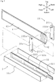
- Fig. 4 illustrates an exploded perspective view of the sensor element.
- Fig. 5 illustrates a cross-section view in a transverse direction in Fig. 4 near an electrode on the left side.
- a constraining plate and an insulation film are transparently illustrated.
- transparently visible portions are illustrated using thin lines.
- the body unit 300 of the sensor element 30 includes a constraining plate 31, the sensor thin film 32, electrodes 33R and 33L, the wirings 34R and 34L, an insulation film 35, a cover film 36, an elastic plate 37, and a load transmitting plate 38.
- the sensor thin film 32, the electrodes 33R and 33L, the wirings 34R and 34L, the insulation film 35, and the cover film 36 are all formed on the rear side of the constraining plate 31 by using a screen printing method.
- the constraining plate 31 is made of polyethylene terephthalate (PET), and has a belt-like shape extending in the left-right direction.
- PET polyethylene terephthalate
- the electrodes 33R and 33L have a square shape, and are formed on the rear surface of the constraining plate 31.
- the electrodes 33R and 33L are interposed between the constraining plate 31 and the sensor thin film 32.
- the electrode 33R is arranged on the right end of the sensor thin film 32, and the electrode 33L is arranged on the left end of the sensor thin film 32.
- the wirings 34R and 34L are formed on the rear surface of the constraining plate 31.
- the wiring 34R is connected to the electrode 33R, and the wiring 34L is connected to the electrode 33L.
- the electrodes 33R and 33L and the wirings 34R and 34L are all formed from silver paste.
- the insulation film 35 is made of acrylic resin, and has a belt-like shape extending in the left-right direction.
- the insulation film 35 covers the rear surface of the constraining plate 31 in a state excluding the electrodes 33R and 33L.
- the constraining plate 31 and the insulation film 35 are included in a base material in the present invention.
- the sensor thin film 32 has a belt-like shape extending in the left-right direction.
- the sensor thin film 32 has a film thickness of about 250 ⁇ m.
- the sensor thin film 32 is arranged on the rear surface of the constraining plate 31, more specifically, on the rear surface of the electrodes 33R and 33L and the insulation film 35.
- the sensor thin film 32 is formed in which carbon beads (conductive filler) are filled in epoxy resin. The filling rate of the carbon beads is about 45% by volume when the volume of the sensor thin film 32 is 100% by volume.
- the cover film 36 is made of acrylic rubber, and has a belt-like shape extending in the left-right direction.
- the cover film 36 covers the rear surfaces of the insulation film 35 and the sensor thin film 32.
- the elastic plate 37 is made of acrylic rubber, and has a flat plate-like shape extending in the left-right direction.
- the elastic plate 37 has a thickness of about 3 mm.
- the elastic plate 37 has a width (length in the up-down direction) of about the same as that of the constraining plate 31. Further, the elastic plate 37 has a length (length in the left-right direction) of about the same as that of the body unit 300.
- the elastic plate 37 is arranged on the rear side of the constraining plate 31. The elastic plate 37 and the cover film 36 are bonded together.
- the load transmitting plate 38 is made of an acrylonitrile-butadiene-styrene (ABS) resin, and has a flat plate-like shape extending in the left-right direction.
- the load transmitting plate 38 has dimensions of about the same as that of the elastic plate 37.
- the load transmitting plate 38 is arranged on the front surface of the constraining plate 31.
- the load transmitting plate 38 and the constraining plate 31 are bonded together.
- the load transmitting plate 38 has a planar front surface and a wave-shaped rear surface. That is, the rear surface is formed with a plurality of convex portions 380 each having a curved surface shape of a same curvature.
- the convex portions 380 and the constraining plate 31 are in line contact.
- the two sheets of laminate film 41 and 42 each have a three-layer structure of outer resin layer / metal foil / inner resin layer.
- the laminate film 41 and the laminate film 42 have the same configuration. Therefore, here, only the configuration of the laminate film 41 is explained.
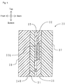
- Fig. 6 illustrates a cross-section view of the laminate film 41.
- the laminate film 41 has an outer resin layer 410, a metal foil 411 and an inner resin layer 412.
- the outer resin layer 410 is made from polyethylene naphthalate (PEN) and forms the outermost layer of the exterior packaging bag 40.
- the outer resin layer 410 has a thickness of about 12 ⁇ m.
- the inner resin layer 412 is made from polypropylene (PP) and forms the innermost layer of the exterior packaging bag 40.
- the inner resin layer 412 has a thickness of about 40 ⁇ m.
- the metal foil 411 is made from aluminum (Al) and is interposed between the outer resin layer 410 and the inner resin layer 412.
- the metal foil 411 has a thickness of about 7 ⁇ m.
- the exterior packaging bag 40 having one opening side is prepared by superimposing the two sheets of laminate films 41 and 42 and heat fusion bonding three surrounding edges.
- the body unit 300 of the sensor element 30 is housed in the exterior packaging bag 40.
- the wiring unit 301 projects out from the exterior packaging bag 40.
- the exterior packaging bag 40 is deaerated, and the opening of the exterior packaging bag 40 is sandwiched using the packing member 20 and sealed.
- the sensor assembly 3 is prepared.
- the prepared sensor assembly 3 together with the packing member 20 are installed to the assembly mounting opening 220 of the case body 22 of the circuit case 2.
- the wiring unit 301 is inserted into the inside of the case body 22.
- the wiring unit 301 is connected to the connector 21.
- the surrounding of the wiring unit 301 is secured using a sealant material.
- the load is divided by the convex portions 380 of the load transmitting plate 38, and is transmitted to the sensor element 30. That is, the constraining plate 31 and the sensor thin film 32 are depressed by the convex portions 380 of a certain curvature.
- the film thickness of the sensor thin film 32 is small. For this reason, the sensor thin film 32 almost does not compressively deform. Further, deformation of the front surface of the sensor thin film 32 is restricted by the constraining plate 31.
- the elastic plate 37 compressively deforms in such a manner as to compress in the front-rear direction. Along with this, the sensor thin film 32 bends in such a manner as to deflect backward.
- Data such as the electrical resistance, voltage, and the like of the sensor thin film 32 are sent via the wirings 34R and 34L, the connector 21, the circuit substrate 24 and the external connection connector 23 to the external occupant protection ECU, and are processed.
- the sensor module 1 detects an input load based on an increase in the electrical resistance of the sensor thin film 32.
- the wiring unit 301 of the sensor element 30 is housed inside the case body 22 of the circuit case 2. For this reason, the wiring unit 301 is unlikely to be damaged by an impact and the like. Further, the circuit case 2 is sealed. For this reason, deterioration of the wiring unit 301 is inhibited. Further, the opening of the exterior packaging bag 40 on the left edge is sealed by the packing member 20 inside the case body 22. This inhibits penetration of oxygen and moisture into the exterior packaging bag 40 via the opening. Thus, deterioration of the body unit 300 of the sensor element 30 is inhibited. Therefore, the sensor module 1 according to the present embodiment is superior in durability and ensures a long life.
- the outer resin layer 410 of the exterior packaging bag 40 is made from polyethylene naphthalate (PEN), and the inner resin layer 412 of the exterior packaging bag 40 is made from polypropylene (PP).
- PEN polyethylene naphthalate
- PP polypropylene
- PEN has superior heat and humidity resistance, heat resistance, and chemical resistance. Therefore, the exterior packaging bag 40 has high heat and humidity resistance, heat resistance, and chemical resistance.
- PP has a melting point lower than that of PEN. Therefore, by heat fusion bonding, the laminate films 41 and 42 can be easily bonded.
- the metal foil 411 of the exterior packaging bag 40 is made of aluminum (Al). Al has a superior moisture-proof property and is also highly conductive. For this reason, a socalled Faraday cage can be formed surrounding the body unit 300. Therefore, an electromagnetic wave generated by the body unit 300 can be inhibited from leaking to the outside of the exterior packaging bag 40. Therefore, noise in the electrical circuit can be reduced. By grounding the metal foil 411, the electromagnetic wave can
- a load is divided by the convex portions 380 of the load transmitting plate 38 to be input to the sensor thin film 32.
- the convex portions 380 are formed in a curved surface shape of a predetermined curvature. For this reason, when a load is input to the sensor thin film 32, the shape of the colliding object is hardly reflected. Further, a bending deformation of the sensor thin film 32 is induced by the constraining plate 31 and the elastic plate 37. That is, the energy of the input load is used on bending the sensor thin film 32. Therefore, according to the sensor assembly 3, by measuring the change in the electrical resistance based on the bending deformation of the sensor thin film 32, the load can be accurately detected regardless of the size and shape of the colliding object.
- the insulation plate 60a is made of silicone rubber and has a belt-like shape extending in the left-right direction.
- the insulation plate 60a has a width (length in the up-down direction) of about the same as that of the body unit 500 of the sensor element 50. Further, the insulation plate 60a has a length (length in the left-right direction) of about the same as that of the body unit 500 of the sensor element 50.
- the insulation plate 60a is arranged on the front side of the body unit 500 of the sensor element 50.
- the insulation plate 60b is made of silicone rubber and has a belt-like shape extending in the left-right direction.
- the insulation plate 60b has a width (length in the up-down direction) of about the same as that of the body unit 500 of the sensor element 50. Further, the insulation plate 60b has a length (length in the left-right direction) of about the same as that of the body unit 500 of the sensor element 50.
- the insulation plate 60b is arranged on the rear side of the body unit 500 of the sensor element 50.
- the wiring 53a connects to each of the electrodes 52a formed on the front surface of the sensor thin film 51.
- the wiring 53a is formed on the front surface of the sensor thin film 51 by using screen printing.
- the wiring 53b connects to each of the electrodes 52b (illustrated by dotted lines in Fig. 8 ) formed on the rear surface of the sensor thin film 51.
- the wiring 53b is formed on the rear surface of the sensor thin film 51 by using screen printing.
- the wirings 53a and 53b are formed from an elastomeric material in which silver powder is filled in urethane rubber.
- the cover film 54a is made of acrylic rubber, and has a belt-like shape extending in the left-right direction.
- the cover film 54a covers the front surface of the sensor thin film 51, the electrodes 52a, and the wiring 53a.
- the cover film 54b is made of acrylic rubber, and has a belt-like shape extending in the left-right direction.
- the cover film 54b covers the rear surface of the sensor thin film 51, the electrodes 52b, and the wiring 53b.
- the film member 61b has a width (length in the up-down direction) of about the same as that of the body unit 300 of the sensor element 30. Further, the film member 61b has a length (length in the left-right direction) of about the same as that of the body unit 300 of the sensor element 30. The film member 61b is arranged on the rear side of the body unit 300 of the sensor element 30.
- the sensor module according to the present embodiment is installed on the back side (rear side) of the front bumper so that a load is input to the sensor assembly via the front bumper. Therefore, in the present embodiment, directions in the above-mentioned Fig. 1 are defined so that the front and rear sides are reversed.
- a load is input from front to the front bumper. Thereafter, along with the deformation of the front bumper, the load is transmitted to the sensor assembly. That is, the load is input to the sensor element from the side of a base material, which will be described later.
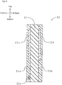
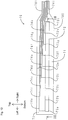
- Fig. 12 illustrates a rear view of the sensor element in the sensor assembly according to the present embodiment.
- Fig. 13 illustrates a cross-section view along a line XIII-XIII in Fig. 12 .
- Fig. 14 illustrates an enlarged view within a circle XIV in Fig. 13 .
- the cover film is illustrated with the right half removed.
- the sensor element 70 has a body unit 700 and a wiring unit 701.
- the body unit 700 has a sensor thin film 72, which will be described later.
- the body unit 700 detects deformation of the front bumper (measured object).
- the body unit 700 is enclosed in the exterior packaging bag 40 (see above-mentioned Fig. 1 ).
- the wiring unit 701 has wirings 74a-74i, which will be described later.
- the wiring unit 701 projects out from the exterior packaging bag 40 toward the right side.
- the sensor thin film 72 has a belt-like shape extending in the left-right direction.
- the sensor thin film 72 has a film thickness of about 100 ⁇ m.
- the sensor thin film 72 is secured on the rear surface of the base material 71.
- the sensor thin film 72 is formed in which carbon beads (conductive filler) are filled in epoxy resin.
- the filling rate of the carbon beads is about 45% by volume when the volume of the sensor thin film 72 is 100% by volume.
- Fig. 14 schematically illustrates, in the sensor thin film 72, a plurality of cracks C1 are formed in advance.
- the cracks C1 are arranged extending in a direction intersecting the arrangement direction (left-right direction) of the electrodes 73a - 73i, that is, in the thickness direction (front-rear direction) of the sensor thin film 72. About two of the cracks C1 are formed in each unit section U1 of about 2 mm along the left-right direction of the sensor thin film 72.
- the production method of the sensor element 70 includes a coating material preparation process, a printing process, a bending curing process, an unloading process, and a cover film forming process.
- coating materials for forming the sensor thin film 72, the electrodes 73a - 73i, the wirings 74a - 74i, and the cover film 75 are respectively prepared.
- coating materials, except a cover film coating material are printed on the surface of the base material using screen printing equipment.
- an electrode coating material and a wiring coating material are sequentially printed.
- the coated film is cured, and the electrodes 73a - 73i and the wirings 74a - 74i are formed.
- a sensor coating material is printed on the surface of the base material 71 on which the electrodes 73a - 73i are formed.
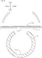
- Fig. 15 illustrates a schematic view of a first half of the bending curing process.
- Fig. 16 illustrates a schematic view of a second half of the bending curing process.
- the base material 71 on which the coated film 720 of the sensor coating material is formed is applied to an inner periphery 760 of a C-shaped mold 76.
- a front surface 710 of the base material 71 is in contact with the inner periphery 760 of the mold 76.
- the mold 76 is placed in a drying furnace and kept for 1 hour at a temperature of about 140 °C to subject the coated film 720 to a primary curing.
- the coated film 720 is kept for 2 hours at a temperature of about 170 °C to subject the coated film 720 to a secondary curing.
- the base material 71 together with the cured coated film 720 are peeled off from the mold 76, and the base material 71 and the cured coated film 720 are restored from the bent state to their original planar state (see above-mentioned Fig. 15 ).
- a strain is input to the cured coated film 720 (sensor thin film 72) and cracks are formed therein. As described above, the sensor thin film 72 is formed.
- the sensor assembly and the sensor module according to the present embodiment have the same operation effects as the sensor assembly and the sensor module according to the first embodiment with respect to the portions having common configurations.
- the bending of the sensor thin film 72 causes the cracks C1 to open up. This causes the conductive paths to be cut off and the electrical resistance of the sensor thin film 72 to rapidly increase. Therefore, response delay is small.
- the conductive paths are cut off primarily due to opening up of the cracks C1. Therefore, as compared to the case where the cutting off of the conductive paths depends only on the elastic deformation of the parent material (see above-mentioned Fig. 17 ), even a small strain can be detected with a good accuracy.
- the response speed is less dependent on atmospheric temperature and the input speed of a strain.
- the sensor thin film 72 is covered by the cover film 75. This inhibits deterioration of the sensor thin film 72. Further, when the load is removed after the bending deformation, with the help of the elastic restoring force of the cover film 75, the sensor thin film 72 easily restores its original shape.
- the exterior packaging bag is formed from a laminate film having a PEN/Al/PP three-layer structure.
- the configuration of the laminate film is not limited to the above embodiments.
- the resin of the outer resin layer polyphenylene sulfide (PPS), polyethylene terephthalate (PET), polyethylene (PE), polypropylene (PP), polyamide (PA), polycarbonate (PC), polyoxymethylene (POM), polymethylmethacrylate (PMMA), polyvinyl chloride resin (PVC), fluorine resin (polytetrafluoroethylene (PTFE), tetrafluoroethylene-ethylene copolymer (ETFE), and the like), ethylene-vinyl alcohol copolymer resin (EVOH), and the like, may be used.
- PPS polyphenylene sulfide
- PET polyethylene terephthalate
- PE polyethylene
- PP polypropylene
- PA polyamide
- PC polycarbonate
- POM polyoxymethylene
- PMMA polymethylme
- the metal foil tin, copper, stainless steel, zinc, and the like
- the resin of the inner resin layer similar to the outer resin layer, PPS, PET, PE, PP, PA, PC, POM, PMMA, PVC, fluorine resin (PTFE, ETFE, and the like), EVOH, and the like, may be used. It is desirable that a resin used for the inner resin layer have a melting point lower than that of the outer resin layer. Further, as needed, other layers may be laminated on the above three layers to form a structure of four or more layers. Further, thickness of each layer is not particularly limited.
- a sensor element is used in which electrical resistance of the sensor thin film changes due to a deformation.
- a sensor element is used in which capacitance changes due to a deformation.
- the type, configuration, shape, size, and the like of the sensor element are not limited to the above embodiments.
- the parent material of the sensor thin film may be suitably selected from resin and elastomer, by taking into account compatibility with the conductive filler.
- the number of the electrodes and arrangement locations may be suitably set.
- the base material (including the constraining plate and the insulation films) and the material of the cover film are not particularly limited as long as they are insulating materials. It is desirable that the base material be a material that can restrict a deformation of one side of the sensor thin film.
- flexible resin films such as PE, PEN and the like are preferred.
- the insulation film and cover film are not arranged.
- the material, shape, and the like of the elastic plate and the load transmitting plate are not particularly limited.
- the convex portions all have the same curvature.
- the curvature of the convex portions By varying the curvature of the convex portions, the relation between a load and an output can be adjusted.
- the greater the curvature of the convex portions of the load transmitting plate is, the greater the amount of bending deformation of the sensor thin film due to depressing by the convex portions will be. Therefore, detection sensitivity of a load can be improved.
- the number of the convex portions may be suitably determined by taking into account the shape and size of an anticipated colliding object. The greater the number of convex portions is, the more finely the shape of the colliding object can be divided. For this reason, dependence on the shape of the colliding object can be further reduced. It is also possible that the elastic plate and the load transmitting plate are not arranged.
- the method for forming the cracks in the sensor thin film is not particularly limited.
- the sensor thin film be further subjected to bending processing. By doing so, cracks can be increased in number and can be dispersed in the parent material. Further, by devising distribution and the like of the convexo-concave portions to be formed, distribution of the cracks and the like can be adjusted.
- the type of the elastomer of the sensor thin film is not particularly limited.
- a material having a large relative permittivity is preferred.
- the electrodes and wirings be flexible and deformable together with the sensor thin film.
- three pairs of opposing electrodes are formed across the sensor thin film.
- the number, size, arrangement, and the like of the electrodes may be suitably determined according to an intended use.
- the electrodes and wirings are formed on the front surface and rear surface of the sensor thin film, respectively.
- the sensor thin film, the electrodes, and the wirings may also be formed on a surface of an insulating base material. It is also possible that the cover film is not arranged.
- the material of the insulation plate is not particularly limited as long as it is an insulating material. Various elastomers, including silicone rubber, can be used.
- the material of the film member is not particularly limited. From a point of view of having a small friction coefficient, in addition to POM, fluorine resin such as PTFE and ETFE are preferable.
- one edge of the exterior packaging bag is sealed by using the packing member.
- the shape, material, and the like of the packing member are not particularly limited.
- the shape and material of the circuit case, as well as the manner in which the circuit case connects to an external electronic device, and the like, are not particularly limited.
- Heat and humidity resistance of the exterior packaging bag used in the above embodiments was experimentally evaluated.
- three kinds of exterior packaging bags having different kinds of outer resin layers were prepared.
- One of the outer resin layers of the three kinds of exterior packaging bags was made of polyethylene naphthalate (PEN), which was the same as in the above embodiments.
- the remaining two were respectively made of polyphenylene sulfide (PPS) and polyethylene terephthalate (PET).
- the outer resin layers all had a thickness of 12 ⁇ m. Configurations other than the outer resin layers of the exterior packaging bags were the same as in the above embodiments.
- a temperature and humidity sensor was placed in each of the exterior packaging bags, and after deaeration, the opening was sealed using the packing member.
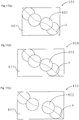
- Fig. 11 illustrates measurement results of the humidity inside the exterior packaging bags.
- Fig. 11 illustrates, in all of the exterior packaging bags, the internal humidity was maintained at 5% or less.
- the internal temperature was constant at about 85 °C.
- the exterior packaging bag formed from the laminate film having a structure of resin layer / metal foil / resin layer has superior heat and humidity resistance. Therefore, by enclosing a component such as a sensor element and the like in the exterior packaging bag, deterioration of the sensor component in a hot and humid environment can be inhibited. That is, the sensor assembly and the sensor module according to the present invention have superior heat and humidity resistance and ensure a long life.
- the sensor assembly and the sensor module according to the present invention can be applied to various applications including a collision sensor in an automobile and the like; a soft pressure sensor such as a seating sensor and artificial skin; a data input device such as a keyboard; a surface pressure distribution sensor for a bed and a carpet; and the like.
Landscapes
- Physics & Mathematics (AREA)
- General Physics & Mathematics (AREA)
- Measurement Of Length, Angles, Or The Like Using Electric Or Magnetic Means (AREA)
- Force Measurement Appropriate To Specific Purposes (AREA)
- Seats For Vehicles (AREA)
Claims (6)
- Sensoranordnung (3), die umfasst:ein Sensorelement (30; 50; 70); undeine Außenbeutelverpackung (40), die das Sensorelement (30; 50; 70) umschließt, wobei das Sensorelement (30; 50; 70) umfasst:eine aus Harz oder Elastomer hergestellte Sensordünnschicht (32; 51; 72); undwenigstens ein Elektrodenpaar (33R, 33L; 52a, 52b; 73a - 73i), das mit der Sensordünnschicht (32; 51; 72) verbunden ist,dadurch gekennzeichnet, dassdie Außenbeutelverpackung (40) aus einer Laminatdünnschicht (41, 42) hergestellt ist, die eine Metallfolie (411) und zwei Harzschichten (410, 412) hat, welche derart angeordnet sind, dass sie die Metallfolie (411) eingeschoben haben,die Sensordünnschicht (32; 51; 72) aus Elastomer hergestellt ist;das Elektrodenpaar (33R, 33L; 52a, 52b; 73a - 73i) auf einer oder beiden Seiten der Sensordünnschicht (32; 51; 72) angeordnet ist; unddas Sensorelement (30; 50; 70) konfiguriert ist, um eine Eingangslast basierend auf einer Kapazitätsänderung zwischen dem Elektrodenpaar (33R, 33L; 52a, 52b; 73a - 73i) zu erfassen.
- Sensoranordnung (3) nach Anspruch 1, wobei von den zwei Harzschichten (410, 412) eine innere Harzschicht (412), die auf einer Innenseite angeordnet ist, einen niedrigeren Schmelzpunkt als den einer äußeren Harzschicht (410) hat, die auf einer Außenseite angeordnet ist.
- Sensoranordnung (3) nach Anspruch 2, wobei die äußere Harzschicht (412) aus wenigstens einer Art hergestellt ist, die ausgewählt wird aus: Polyphenylensulfid, Polyethylenterephthalat, Polyethylennaphthalat, Polyethylen, Polypropylen, Polyamid, Polykarbonat, Polyoxymethylen, Polymethylmethacrylat, Polyvinylchloridharz, Fluorharz und Ethylenvinylalkohol-Copolymerharz.
- Sensoranordnung (3) nach Anspruch 1, wobei die Metallfolie (411) aus wenigstens einer Art hergestellt ist, die ausgewählt wird aus: Aluminium, Zinn, Kupfer, nichtrostendem Stahl und Zink.
- Sensoranordnung (3) nach Anspruch 1, wobei ein Dünnschichtelement (60a, 60b; 61 a, 61 b) zwischen der Außenbeutelverpackung (40) und dem Sensorelement (50) eingefügt ist, wobei das Dünnschichtelement (60a, 60b; 61 a, 61 b) einen kleineren Reibungskoeffizienten als den einer Innenfläche der Außenbeutelverpackung (40) und/oder einer äußersten Fläche des Sensorelements (50) hat.
- Sensormodul (1), das umfasst:die Sensoranordnung (3) nach einem der Ansprüche 1 - 5; undein Schaltungsgehäuse (2), auf dem die Sensoranordnung (3) installiert ist, wobeidie Außenbeutelverpackung (40) der Sensoranordnung (3) eine Öffnung hat;das Sensorelement (30; 50; 70) eine Verdrahtungseinheit (301) hat, die von der Öffnung aus der Außenbeutelverpackung (40) vorsteht; unddas Schaltungsgehäuse (3) eine kastenartige Form hat und umfasst:einen Gehäusekörper (22), auf dem eine Anordnungsmontageöffnung (220) bereitgestellt ist;ein Dichtungselement (20), das die Öffnung in einem Zustand, in dem die Verdrahtungseinheit (301) von der Öffnung der Außenbeutelverpackung (40) vorsteht abdichtet und auf der Anordnungsmontageöffnung (220) des Gehäusekörpers (22) installiert ist; undeinen Verbinder (21), der mit der Verdrahtungseinheit (301) im Inneren des Gehäusekörpers (22) und mit einer elektrischen Schaltung (24) verbunden ist.
Applications Claiming Priority (2)
| Application Number | Priority Date | Filing Date | Title |
|---|---|---|---|
| JP2009222119 | 2009-09-28 | ||
| PCT/JP2010/066130 WO2011037078A1 (ja) | 2009-09-28 | 2010-09-17 | センサアセンブリおよびセンサモジュール |
Publications (3)
| Publication Number | Publication Date |
|---|---|
| EP2461146A1 EP2461146A1 (de) | 2012-06-06 |
| EP2461146A4 EP2461146A4 (de) | 2014-10-15 |
| EP2461146B1 true EP2461146B1 (de) | 2017-06-14 |
Family
ID=43795826
Family Applications (1)
| Application Number | Title | Priority Date | Filing Date |
|---|---|---|---|
| EP10818751.9A Not-in-force EP2461146B1 (de) | 2009-09-28 | 2010-09-17 | Sensoranordnung und sensormodul |
Country Status (4)
| Country | Link |
|---|---|
| US (1) | US8770045B2 (de) |
| EP (1) | EP2461146B1 (de) |
| JP (1) | JPWO2011037078A1 (de) |
| WO (1) | WO2011037078A1 (de) |
Families Citing this family (12)
| Publication number | Priority date | Publication date | Assignee | Title |
|---|---|---|---|---|
| JP5486683B2 (ja) * | 2010-11-04 | 2014-05-07 | 東海ゴム工業株式会社 | 曲げセンサ |
| JP5759612B2 (ja) | 2012-03-02 | 2015-08-05 | 住友理工株式会社 | ハイブリッドセンサ |
| DE102012016238B4 (de) * | 2012-08-16 | 2020-01-02 | GM Global Technology Operations LLC (n. d. Ges. d. Staates Delaware) | Verfahren zur Beseitigung von elektrischen Kurzschlüssen und Diagnosegerät |
| DE102012217086B3 (de) * | 2012-09-21 | 2014-03-20 | Mayser Gmbh & Co. Kg | Kapazitiver Sensor und Tür- oder Klappenanordnung mit einem kapazitivem Sensor |
| DE102012217083A1 (de) | 2012-09-21 | 2014-03-27 | Mayser Gmbh & Co. Kg | Tür- oder Klappenanordnung |
| JP2014115232A (ja) * | 2012-12-11 | 2014-06-26 | Dmt:Kk | 磁気検出プローブ及び磁気検出プローブの製造方法 |
| US9127968B2 (en) | 2013-11-18 | 2015-09-08 | Ford Global Technologies, Llc | Flexible optical impact detection sensor for front rail mounted airbag |
| US9004216B1 (en) | 2013-11-18 | 2015-04-14 | Ford Global Technologies, Llc | Front rail mounted airbag |
| RU2589494C1 (ru) * | 2015-03-11 | 2016-07-10 | Федеральное государственное унитарное предприятие "Центральный аэрогидродинамический институт имени профессора Н.Е. Жуковского" (ФГУП "ЦАГИ") | Ёмкостной инерционный датчик давления, способ его сборки и способ измерения давления |
| JP6503815B2 (ja) * | 2015-03-19 | 2019-04-24 | 大日本印刷株式会社 | 圧力センサ |
| DE102016221895A1 (de) * | 2016-11-08 | 2018-05-09 | Brose Fahrzeugteile Gmbh & Co. Kommanditgesellschaft, Bamberg | Verfahren zur Abdichtung einer Sensorelektrode |
| WO2018093275A1 (en) * | 2016-11-17 | 2018-05-24 | Stretchsense Limited | A stretch sensor with an improved flexible interconnect |
Citations (1)
| Publication number | Priority date | Publication date | Assignee | Title |
|---|---|---|---|---|
| JP2002350250A (ja) * | 2001-03-19 | 2002-12-04 | Auto Network Gijutsu Kenkyusho:Kk | センサユニット、センサ取付用袋体およびセンサ取付方法 |
Family Cites Families (24)
| Publication number | Priority date | Publication date | Assignee | Title |
|---|---|---|---|---|
| JPS6241531A (ja) | 1985-08-16 | 1987-02-23 | Nippon Alum Mfg Co Ltd:The | 天井空調装置 |
| JPH0219226Y2 (de) | 1985-08-19 | 1990-05-28 | ||
| DE3841243A1 (de) * | 1988-12-07 | 1990-06-13 | Brunner Wolfgang | Messanordnung, vorzugsweise in form einer messplattform |
| JP3023730B2 (ja) * | 1992-04-02 | 2000-03-21 | 富士写真フイルム株式会社 | 写真感光材料用包装材料及びこれを用いた包装袋 |
| JP3201837B2 (ja) * | 1992-08-03 | 2001-08-27 | 博明 柳田 | 導電性繊維束含有プラスチック複合材による歪・応力探知方法およびそれに用いる導電性繊維束含有プラスチック複合材 |
| JP3482583B2 (ja) * | 1996-04-30 | 2003-12-22 | 株式会社ケーヒン | 圧力検知機の防水構造 |
| TW460485B (en) * | 1998-06-19 | 2001-10-21 | Japan Polyolefins Co Ltd | Ethylene.Α-olefin copolymer, and combinations, films and use thereof |
| JP2000088677A (ja) | 1998-09-09 | 2000-03-31 | Kinugawa Rubber Ind Co Ltd | 感圧センサ |
| JP3881812B2 (ja) * | 1999-08-27 | 2007-02-14 | 関東自動車工業株式会社 | 着座センサ |
| JP2004239691A (ja) * | 2003-02-04 | 2004-08-26 | Auto Network Gijutsu Kenkyusho:Kk | 感圧センサ及び該感圧センサの座席シートへの取付方法 |
| US7834527B2 (en) * | 2005-05-05 | 2010-11-16 | SmartMotion Technologies, Inc. | Dielectric elastomer fiber transducers |
| JP4311744B2 (ja) | 2005-12-02 | 2009-08-12 | 株式会社デンソー | 衝突検出装置 |
| JP5302501B2 (ja) | 2006-10-25 | 2013-10-02 | 東海ゴム工業株式会社 | 車両の外装部材変形センサ |
| DE602007013162D1 (de) | 2006-10-25 | 2011-04-28 | Tokai Rubber Ind Ltd | Verformungssensor |
| JP5006018B2 (ja) * | 2006-12-13 | 2012-08-22 | 学校法人自治医科大学 | 生体情報計測用パネル及びそれを用いた生体情報計測システム |
| JP2008175659A (ja) | 2007-01-18 | 2008-07-31 | Yokogawa Electric Corp | 圧力センサ |
| JP4508199B2 (ja) * | 2007-02-05 | 2010-07-21 | ソニー株式会社 | リード用シーラントフィルム及び非水電解質電池 |
| JP4978484B2 (ja) * | 2007-02-16 | 2012-07-18 | セイコーエプソン株式会社 | 防水型電子機器 |
| JP5496446B2 (ja) | 2007-07-12 | 2014-05-21 | 東海ゴム工業株式会社 | 静電容量型センサ |
| JP2009198483A (ja) * | 2008-01-24 | 2009-09-03 | Tokai Rubber Ind Ltd | センサ薄膜、その製造方法、および変形センサ |
| JP2009200006A (ja) | 2008-02-25 | 2009-09-03 | Nissan Motor Co Ltd | 燃料電池システムおよび燃料電池システムの制御方法 |
| US8272276B2 (en) * | 2009-05-06 | 2012-09-25 | Xsensor Technology Corporation | Dielectric textured elastomer in a pressure mapping system |
| JP4890589B2 (ja) * | 2009-05-25 | 2012-03-07 | 本田技研工業株式会社 | 車両用衝突検出装置 |
| CN102272566B (zh) | 2009-11-24 | 2013-09-25 | 东海橡塑工业株式会社 | 弯曲传感器及变形形状测量方法 |
-
2010
- 2010-09-17 WO PCT/JP2010/066130 patent/WO2011037078A1/ja not_active Ceased
- 2010-09-17 JP JP2011532986A patent/JPWO2011037078A1/ja active Pending
- 2010-09-17 EP EP10818751.9A patent/EP2461146B1/de not_active Not-in-force
-
2012
- 2012-02-21 US US13/401,300 patent/US8770045B2/en active Active
Patent Citations (1)
| Publication number | Priority date | Publication date | Assignee | Title |
|---|---|---|---|---|
| JP2002350250A (ja) * | 2001-03-19 | 2002-12-04 | Auto Network Gijutsu Kenkyusho:Kk | センサユニット、センサ取付用袋体およびセンサ取付方法 |
Also Published As
| Publication number | Publication date |
|---|---|
| US20120144935A1 (en) | 2012-06-14 |
| WO2011037078A1 (ja) | 2011-03-31 |
| JPWO2011037078A1 (ja) | 2013-02-21 |
| EP2461146A4 (de) | 2014-10-15 |
| US8770045B2 (en) | 2014-07-08 |
| EP2461146A1 (de) | 2012-06-06 |
Similar Documents
| Publication | Publication Date | Title |
|---|---|---|
| EP2461146B1 (de) | Sensoranordnung und sensormodul | |
| US8986861B2 (en) | Electricity accumulation device | |
| EP2381233B1 (de) | Biegungssensor und verfahren zur messung einer verformten form | |
| CN104067099B (zh) | 静电电容式传感器 | |
| JP5486683B2 (ja) | 曲げセンサ | |
| EP2015043B1 (de) | Elektrostatische Kapazitätssensor | |
| JP5448423B2 (ja) | 触覚センサおよびその製造方法 | |
| US11387566B2 (en) | Electromagnetic wave absorber and molded article with electromagnetic wave absorber | |
| WO2008059751A1 (en) | Piezoelectric sensor and method for manufacturing the same | |
| JP5654789B2 (ja) | 曲げセンサおよび変形形状測定方法 | |
| JP7213921B2 (ja) | せん断力センサー及びせん断力センサー用の検出部 | |
| JP3652402B2 (ja) | 防水・防滴構造付き電池パック | |
| JP5622471B2 (ja) | 抵抗増加型センサおよびその製造方法 | |
| US10598558B2 (en) | Pressure sensing element | |
| CN211626765U (zh) | 应力应变传感器、应力应变传感模组及电子设备 | |
| US11315809B2 (en) | Device and forming method of device | |
| US11852547B1 (en) | Surface force sensor that senses force applied to a surface from an object attached to the surface | |
| CN113324682A (zh) | 应力应变传感器、应力应变传感模组及电子设备 | |
| JP5448910B2 (ja) | 導電層の形成方法 | |
| JPH0792413B2 (ja) | 触覚センサ | |
| CN117213669A (zh) | 电子皮肤与电子皮肤的制备方法 |
Legal Events
| Date | Code | Title | Description |
|---|---|---|---|
| PUAI | Public reference made under article 153(3) epc to a published international application that has entered the european phase |
Free format text: ORIGINAL CODE: 0009012 |
|
| 17P | Request for examination filed |
Effective date: 20120228 |
|
| AK | Designated contracting states |
Kind code of ref document: A1 Designated state(s): AL AT BE BG CH CY CZ DE DK EE ES FI FR GB GR HR HU IE IS IT LI LT LU LV MC MK MT NL NO PL PT RO SE SI SK SM TR |
|
| DAX | Request for extension of the european patent (deleted) | ||
| A4 | Supplementary search report drawn up and despatched |
Effective date: 20140911 |
|
| RIC1 | Information provided on ipc code assigned before grant |
Ipc: G01L 1/20 20060101AFI20140905BHEP |
|
| RAP1 | Party data changed (applicant data changed or rights of an application transferred) |
Owner name: SUMITOMO RIKO COMPANY LIMITED |
|
| GRAP | Despatch of communication of intention to grant a patent |
Free format text: ORIGINAL CODE: EPIDOSNIGR1 |
|
| INTG | Intention to grant announced |
Effective date: 20161214 |
|
| GRAS | Grant fee paid |
Free format text: ORIGINAL CODE: EPIDOSNIGR3 |
|
| GRAA | (expected) grant |
Free format text: ORIGINAL CODE: 0009210 |
|
| RIN1 | Information on inventor provided before grant (corrected) |
Inventor name: HAYAKAWA, TOMONORI Inventor name: MURAYAMA, MASARU Inventor name: HASHIMOTO, KAZUNOBU Inventor name: SAITOU, YUUKI |
|
| AK | Designated contracting states |
Kind code of ref document: B1 Designated state(s): AL AT BE BG CH CY CZ DE DK EE ES FI FR GB GR HR HU IE IS IT LI LT LU LV MC MK MT NL NO PL PT RO SE SI SK SM TR |
|
| REG | Reference to a national code |
Ref country code: GB Ref legal event code: FG4D |
|
| REG | Reference to a national code |
Ref country code: CH Ref legal event code: EP Ref country code: AT Ref legal event code: REF Ref document number: 901432 Country of ref document: AT Kind code of ref document: T Effective date: 20170615 |
|
| RIN2 | Information on inventor provided after grant (corrected) |
Inventor name: HASHIMOTO, KAZUNOBU Inventor name: HAYAKAWA, TOMONORI Inventor name: MURAYAMA, MASARU Inventor name: SAITOU, YUUKI |
|
| REG | Reference to a national code |
Ref country code: IE Ref legal event code: FG4D |
|
| REG | Reference to a national code |
Ref country code: DE Ref legal event code: R096 Ref document number: 602010043018 Country of ref document: DE |
|
| REG | Reference to a national code |
Ref country code: NL Ref legal event code: MP Effective date: 20170614 |
|
| REG | Reference to a national code |
Ref country code: LT Ref legal event code: MG4D |
|
| PG25 | Lapsed in a contracting state [announced via postgrant information from national office to epo] |
Ref country code: GR Free format text: LAPSE BECAUSE OF FAILURE TO SUBMIT A TRANSLATION OF THE DESCRIPTION OR TO PAY THE FEE WITHIN THE PRESCRIBED TIME-LIMIT Effective date: 20170915 Ref country code: ES Free format text: LAPSE BECAUSE OF FAILURE TO SUBMIT A TRANSLATION OF THE DESCRIPTION OR TO PAY THE FEE WITHIN THE PRESCRIBED TIME-LIMIT Effective date: 20170614 Ref country code: LT Free format text: LAPSE BECAUSE OF FAILURE TO SUBMIT A TRANSLATION OF THE DESCRIPTION OR TO PAY THE FEE WITHIN THE PRESCRIBED TIME-LIMIT Effective date: 20170614 Ref country code: HR Free format text: LAPSE BECAUSE OF FAILURE TO SUBMIT A TRANSLATION OF THE DESCRIPTION OR TO PAY THE FEE WITHIN THE PRESCRIBED TIME-LIMIT Effective date: 20170614 Ref country code: NO Free format text: LAPSE BECAUSE OF FAILURE TO SUBMIT A TRANSLATION OF THE DESCRIPTION OR TO PAY THE FEE WITHIN THE PRESCRIBED TIME-LIMIT Effective date: 20170914 Ref country code: FI Free format text: LAPSE BECAUSE OF FAILURE TO SUBMIT A TRANSLATION OF THE DESCRIPTION OR TO PAY THE FEE WITHIN THE PRESCRIBED TIME-LIMIT Effective date: 20170614 |
|
| PGFP | Annual fee paid to national office [announced via postgrant information from national office to epo] |
Ref country code: DE Payment date: 20170912 Year of fee payment: 8 |
|
| REG | Reference to a national code |
Ref country code: AT Ref legal event code: MK05 Ref document number: 901432 Country of ref document: AT Kind code of ref document: T Effective date: 20170614 |
|
| PG25 | Lapsed in a contracting state [announced via postgrant information from national office to epo] |
Ref country code: SE Free format text: LAPSE BECAUSE OF FAILURE TO SUBMIT A TRANSLATION OF THE DESCRIPTION OR TO PAY THE FEE WITHIN THE PRESCRIBED TIME-LIMIT Effective date: 20170614 Ref country code: BG Free format text: LAPSE BECAUSE OF FAILURE TO SUBMIT A TRANSLATION OF THE DESCRIPTION OR TO PAY THE FEE WITHIN THE PRESCRIBED TIME-LIMIT Effective date: 20170914 Ref country code: LV Free format text: LAPSE BECAUSE OF FAILURE TO SUBMIT A TRANSLATION OF THE DESCRIPTION OR TO PAY THE FEE WITHIN THE PRESCRIBED TIME-LIMIT Effective date: 20170614 Ref country code: NL Free format text: LAPSE BECAUSE OF FAILURE TO SUBMIT A TRANSLATION OF THE DESCRIPTION OR TO PAY THE FEE WITHIN THE PRESCRIBED TIME-LIMIT Effective date: 20170614 |
|
| PG25 | Lapsed in a contracting state [announced via postgrant information from national office to epo] |
Ref country code: RO Free format text: LAPSE BECAUSE OF FAILURE TO SUBMIT A TRANSLATION OF THE DESCRIPTION OR TO PAY THE FEE WITHIN THE PRESCRIBED TIME-LIMIT Effective date: 20170614 Ref country code: AT Free format text: LAPSE BECAUSE OF FAILURE TO SUBMIT A TRANSLATION OF THE DESCRIPTION OR TO PAY THE FEE WITHIN THE PRESCRIBED TIME-LIMIT Effective date: 20170614 Ref country code: CZ Free format text: LAPSE BECAUSE OF FAILURE TO SUBMIT A TRANSLATION OF THE DESCRIPTION OR TO PAY THE FEE WITHIN THE PRESCRIBED TIME-LIMIT Effective date: 20170614 Ref country code: EE Free format text: LAPSE BECAUSE OF FAILURE TO SUBMIT A TRANSLATION OF THE DESCRIPTION OR TO PAY THE FEE WITHIN THE PRESCRIBED TIME-LIMIT Effective date: 20170614 Ref country code: SK Free format text: LAPSE BECAUSE OF FAILURE TO SUBMIT A TRANSLATION OF THE DESCRIPTION OR TO PAY THE FEE WITHIN THE PRESCRIBED TIME-LIMIT Effective date: 20170614 |
|
| PG25 | Lapsed in a contracting state [announced via postgrant information from national office to epo] |
Ref country code: PL Free format text: LAPSE BECAUSE OF FAILURE TO SUBMIT A TRANSLATION OF THE DESCRIPTION OR TO PAY THE FEE WITHIN THE PRESCRIBED TIME-LIMIT Effective date: 20170614 Ref country code: SM Free format text: LAPSE BECAUSE OF FAILURE TO SUBMIT A TRANSLATION OF THE DESCRIPTION OR TO PAY THE FEE WITHIN THE PRESCRIBED TIME-LIMIT Effective date: 20170614 Ref country code: IS Free format text: LAPSE BECAUSE OF FAILURE TO SUBMIT A TRANSLATION OF THE DESCRIPTION OR TO PAY THE FEE WITHIN THE PRESCRIBED TIME-LIMIT Effective date: 20171014 Ref country code: IT Free format text: LAPSE BECAUSE OF FAILURE TO SUBMIT A TRANSLATION OF THE DESCRIPTION OR TO PAY THE FEE WITHIN THE PRESCRIBED TIME-LIMIT Effective date: 20170614 |
|
| REG | Reference to a national code |
Ref country code: DE Ref legal event code: R097 Ref document number: 602010043018 Country of ref document: DE |
|
| PLBE | No opposition filed within time limit |
Free format text: ORIGINAL CODE: 0009261 |
|
| STAA | Information on the status of an ep patent application or granted ep patent |
Free format text: STATUS: NO OPPOSITION FILED WITHIN TIME LIMIT |
|
| PG25 | Lapsed in a contracting state [announced via postgrant information from national office to epo] |
Ref country code: DK Free format text: LAPSE BECAUSE OF FAILURE TO SUBMIT A TRANSLATION OF THE DESCRIPTION OR TO PAY THE FEE WITHIN THE PRESCRIBED TIME-LIMIT Effective date: 20170614 |
|
| REG | Reference to a national code |
Ref country code: CH Ref legal event code: PL |
|
| 26N | No opposition filed |
Effective date: 20180315 |
|
| GBPC | Gb: european patent ceased through non-payment of renewal fee |
Effective date: 20170917 |
|
| PG25 | Lapsed in a contracting state [announced via postgrant information from national office to epo] |
Ref country code: MC Free format text: LAPSE BECAUSE OF FAILURE TO SUBMIT A TRANSLATION OF THE DESCRIPTION OR TO PAY THE FEE WITHIN THE PRESCRIBED TIME-LIMIT Effective date: 20170614 |
|
| REG | Reference to a national code |
Ref country code: IE Ref legal event code: MM4A |
|
| REG | Reference to a national code |
Ref country code: BE Ref legal event code: MM Effective date: 20170930 |
|
| PG25 | Lapsed in a contracting state [announced via postgrant information from national office to epo] |
Ref country code: LU Free format text: LAPSE BECAUSE OF NON-PAYMENT OF DUE FEES Effective date: 20170917 |
|
| REG | Reference to a national code |
Ref country code: FR Ref legal event code: ST Effective date: 20180531 |
|
| PG25 | Lapsed in a contracting state [announced via postgrant information from national office to epo] |
Ref country code: IE Free format text: LAPSE BECAUSE OF NON-PAYMENT OF DUE FEES Effective date: 20170917 Ref country code: CH Free format text: LAPSE BECAUSE OF NON-PAYMENT OF DUE FEES Effective date: 20170930 Ref country code: LI Free format text: LAPSE BECAUSE OF NON-PAYMENT OF DUE FEES Effective date: 20170930 Ref country code: GB Free format text: LAPSE BECAUSE OF NON-PAYMENT OF DUE FEES Effective date: 20170917 |
|
| PG25 | Lapsed in a contracting state [announced via postgrant information from national office to epo] |
Ref country code: FR Free format text: LAPSE BECAUSE OF NON-PAYMENT OF DUE FEES Effective date: 20171002 Ref country code: BE Free format text: LAPSE BECAUSE OF NON-PAYMENT OF DUE FEES Effective date: 20170930 Ref country code: SI Free format text: LAPSE BECAUSE OF FAILURE TO SUBMIT A TRANSLATION OF THE DESCRIPTION OR TO PAY THE FEE WITHIN THE PRESCRIBED TIME-LIMIT Effective date: 20170614 |
|
| PG25 | Lapsed in a contracting state [announced via postgrant information from national office to epo] |
Ref country code: MT Free format text: LAPSE BECAUSE OF NON-PAYMENT OF DUE FEES Effective date: 20170917 |
|
| REG | Reference to a national code |
Ref country code: DE Ref legal event code: R119 Ref document number: 602010043018 Country of ref document: DE |
|
| PG25 | Lapsed in a contracting state [announced via postgrant information from national office to epo] |
Ref country code: HU Free format text: LAPSE BECAUSE OF FAILURE TO SUBMIT A TRANSLATION OF THE DESCRIPTION OR TO PAY THE FEE WITHIN THE PRESCRIBED TIME-LIMIT; INVALID AB INITIO Effective date: 20100917 |
|
| PG25 | Lapsed in a contracting state [announced via postgrant information from national office to epo] |
Ref country code: DE Free format text: LAPSE BECAUSE OF NON-PAYMENT OF DUE FEES Effective date: 20190402 |
|
| PG25 | Lapsed in a contracting state [announced via postgrant information from national office to epo] |
Ref country code: CY Free format text: LAPSE BECAUSE OF NON-PAYMENT OF DUE FEES Effective date: 20170614 |
|
| PG25 | Lapsed in a contracting state [announced via postgrant information from national office to epo] |
Ref country code: MK Free format text: LAPSE BECAUSE OF FAILURE TO SUBMIT A TRANSLATION OF THE DESCRIPTION OR TO PAY THE FEE WITHIN THE PRESCRIBED TIME-LIMIT Effective date: 20170614 |
|
| PG25 | Lapsed in a contracting state [announced via postgrant information from national office to epo] |
Ref country code: TR Free format text: LAPSE BECAUSE OF FAILURE TO SUBMIT A TRANSLATION OF THE DESCRIPTION OR TO PAY THE FEE WITHIN THE PRESCRIBED TIME-LIMIT Effective date: 20170614 |
|
| PG25 | Lapsed in a contracting state [announced via postgrant information from national office to epo] |
Ref country code: PT Free format text: LAPSE BECAUSE OF FAILURE TO SUBMIT A TRANSLATION OF THE DESCRIPTION OR TO PAY THE FEE WITHIN THE PRESCRIBED TIME-LIMIT Effective date: 20170614 |
|
| PG25 | Lapsed in a contracting state [announced via postgrant information from national office to epo] |
Ref country code: AL Free format text: LAPSE BECAUSE OF FAILURE TO SUBMIT A TRANSLATION OF THE DESCRIPTION OR TO PAY THE FEE WITHIN THE PRESCRIBED TIME-LIMIT Effective date: 20170614 |