EP2461623B1 - Verfahren und system zur verbesserung der signalqualität - Google Patents
Verfahren und system zur verbesserung der signalqualität Download PDFInfo
- Publication number
- EP2461623B1 EP2461623B1 EP09848618.6A EP09848618A EP2461623B1 EP 2461623 B1 EP2461623 B1 EP 2461623B1 EP 09848618 A EP09848618 A EP 09848618A EP 2461623 B1 EP2461623 B1 EP 2461623B1
- Authority
- EP
- European Patent Office
- Prior art keywords
- correction bit
- error rate
- lane
- bit error
- signal
- Prior art date
- Legal status (The legal status is an assumption and is not a legal conclusion. Google has not performed a legal analysis and makes no representation as to the accuracy of the status listed.)
- Active
Links
Images







Classifications
-
- H—ELECTRICITY
- H04—ELECTRIC COMMUNICATION TECHNIQUE
- H04L—TRANSMISSION OF DIGITAL INFORMATION, e.g. TELEGRAPHIC COMMUNICATION
- H04L1/00—Arrangements for detecting or preventing errors in the information received
- H04L1/20—Arrangements for detecting or preventing errors in the information received using signal quality detector
- H04L1/203—Details of error rate determination, e.g. BER, FER or WER
-
- H—ELECTRICITY
- H04—ELECTRIC COMMUNICATION TECHNIQUE
- H04L—TRANSMISSION OF DIGITAL INFORMATION, e.g. TELEGRAPHIC COMMUNICATION
- H04L1/00—Arrangements for detecting or preventing errors in the information received
- H04L1/0001—Systems modifying transmission characteristics according to link quality, e.g. power backoff
- H04L1/0023—Systems modifying transmission characteristics according to link quality, e.g. power backoff characterised by the signalling
- H04L1/0026—Transmission of channel quality indication
-
- H—ELECTRICITY
- H04—ELECTRIC COMMUNICATION TECHNIQUE
- H04L—TRANSMISSION OF DIGITAL INFORMATION, e.g. TELEGRAPHIC COMMUNICATION
- H04L1/00—Arrangements for detecting or preventing errors in the information received
- H04L1/004—Arrangements for detecting or preventing errors in the information received by using forward error control
- H04L1/0045—Arrangements at the receiver end
-
- H—ELECTRICITY
- H04—ELECTRIC COMMUNICATION TECHNIQUE
- H04L—TRANSMISSION OF DIGITAL INFORMATION, e.g. TELEGRAPHIC COMMUNICATION
- H04L1/00—Arrangements for detecting or preventing errors in the information received
- H04L1/004—Arrangements for detecting or preventing errors in the information received by using forward error control
- H04L1/0056—Systems characterized by the type of code used
- H04L1/0071—Use of interleaving
-
- H—ELECTRICITY
- H04—ELECTRIC COMMUNICATION TECHNIQUE
- H04L—TRANSMISSION OF DIGITAL INFORMATION, e.g. TELEGRAPHIC COMMUNICATION
- H04L1/00—Arrangements for detecting or preventing errors in the information received
- H04L1/0078—Avoidance of errors by organising the transmitted data in a format specifically designed to deal with errors, e.g. location
- H04L1/0083—Formatting with frames or packets; Protocol or part of protocol for error control
-
- H—ELECTRICITY
- H04—ELECTRIC COMMUNICATION TECHNIQUE
- H04J—MULTIPLEX COMMUNICATION
- H04J2203/00—Aspects of optical multiplex systems other than those covered by H04J14/05 and H04J14/07
- H04J2203/0001—Provisions for broadband connections in integrated services digital network using frames of the Optical Transport Network [OTN] or using synchronous transfer mode [STM], e.g. SONET, SDH
- H04J2203/0057—Operations, administration and maintenance [OAM]
- H04J2203/006—Fault tolerance and recovery
-
- H—ELECTRICITY
- H04—ELECTRIC COMMUNICATION TECHNIQUE
- H04J—MULTIPLEX COMMUNICATION
- H04J3/00—Time-division multiplex systems
- H04J3/16—Time-division multiplex systems in which the time allocation to individual channels within a transmission cycle is variable, e.g. to accommodate varying complexity of signals, to vary number of channels transmitted
- H04J3/1605—Fixed allocated frame structures
- H04J3/1652—Optical Transport Network [OTN]
-
- H—ELECTRICITY
- H04—ELECTRIC COMMUNICATION TECHNIQUE
- H04L—TRANSMISSION OF DIGITAL INFORMATION, e.g. TELEGRAPHIC COMMUNICATION
- H04L27/00—Modulated-carrier systems
- H04L27/32—Carrier systems characterised by combinations of two or more of the types covered by groups H04L27/02, H04L27/10, H04L27/18 or H04L27/26
- H04L27/34—Amplitude- and phase-modulated carrier systems, e.g. quadrature-amplitude modulated carrier systems
- H04L27/38—Demodulator circuits; Receiver circuits
- H04L27/389—Demodulator circuits; Receiver circuits with separate demodulation for the phase and amplitude components
Definitions
- the present invention relates to the field of communications technologies, and in particular, to a method, a device, and an apparatus for improving signal quality.
- IP traffic increases explosively.
- the optical transport network is becoming IP Internet-oriented, more service-integrated, flexible in resource configuration, and strong in survivability.
- An optical transport system with a high-rate and great capacity will be widely used in the future and the optical transport system with a rate level of 40 G or even 100 G will become the core of the optical transport network in the future.
- the OTN Optical Transport Network, optical transport network
- the procedure of signal processing on the OTN is as follows:
- the optical channel transport unit processing module at a sending end processes a customer signal to obtain an optical channel transport unit frame signal of, and then a physical layer at the sending end modulates data obtained by the optical channel transport unit processing module at the sending end and then transmits the data;
- a physical layer at a receiving end receives and demodulates the transmitted signal, and an optical channel transport unit processing module at the receiving end processes data obtained by the physical layer at the receiving end to restore the optical channel transport unit frame signal, and then processes the optical channel transport unit frame signal to obtain the customer signal transmitted from the sending end on the OTN.
- DWDM dense wavelength division multiplexing
- a new modulation technology is used to compress a transmission frequency band to improve the utilization of the frequency band and to achieve a high performance for the system, which better prevents the impacts from group velocity dispersion and polarization mode dispersion.
- the DP-QOSK dual polarization-quadrature phase shift keying, dual polarization-quadrature phase shift keying
- the DP-QOSK dual polarization-quadrature phase shift keying, dual polarization-quadrature phase shift keying
- the four channels are channel I in an X polarization state, channel Q in the X polarization state, channel I a Y polarization, and channel Q in the Y polarization state.
- an optical module at the receiving end converts the 112 Gbps-signals into two mutually orthogonal polarizations QPSK phase modulated optical signals (that is, a signal in the X polarization state and a signal in the Y polarization state), each signal with a transmission rate of 56 Gbps.
- a QPSK demodulator converts each one of QPSK modulated optical signals into signals on channel I and channel Q, namely, channel I in the X polarization state, channel Q in the X polarization state, channel I in the Y polarization state, and channel Q in the Y polarization state. In this case, four 28 Gbps-signals are obtained.
- the channels on which the 4 signals are transmitted are called physical lanes.
- the signals transmitted on the four physical lanes are de-multiplexed by a 4:10 SerDes (SERializer/DESerializer), and a 10:20 Demux (Demultiplexer) and then aligned and rearranged in a multi lane distribution unit of the optical channel transport unit processing module at the receiving end to restore the optical channel transport unit frame signal. Then, the optical channel transport unit frame signal is processed to restore the customer signal.
- SerDes Serializer/DESerializer
- 10:20 Demux Demultiplexer
- the prior art has the following disadvantages: When the optical module receives and demodulates the optical signals, the demodulated signals are poor in quality because the phases of the signals on channels I and Q in each QPSK demodulation are not completely orthogonal. The poor signal quality affects the subsequent processing. In the prior art, no improvement on the poor signal quality exists, and as a result, a high signal quality may not be obtained.
- WO 02/096003 A1 at best disclose as follows.
- An apparatus and method for dynamically optimizing performance in a communication channel are described.
- the communication channel can be part of a high-speed digital network such as the Internet and can be a dense wavelength-division multiplexed (DWDM) optical communication channel.
- the DWDM signal includes forward error correction (FEC) information which is added to the DWDM signal and is used within the DWDM optical layer to monitor transfer errors in the data.
- FEC forward error correction
- Error correction statistics generated as a result of analysis of the FEC information in the data in accordance with the invention are used in generating an adjustment to and/or optimizing performance of the system.
- the adjustment made can include adjusting power level in one or more of the subsignal transmitters.
- Embodiments of the present invention provide a method, and a system for improving signal quality, which are capable of improving quality of each channel of signals demodulated by an optical module.
- a method for improving signal quality includes:
- An optical transport network apparatus includes:
- the statistic of the error correction bit rate of the data bits of each virtual lane is collected, the pre-correction bit error rate of the physical lane corresponding to each virtual lane is calculated according to the error correction bit rate and then is fed back to the optical module. Then, the optical module can adjust the receiving parameter of each physical lane accordingly to reduce the pre-correction bit error rate of each physical lane, which improves the quality of each channel of signals demodulated by the optical module.
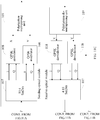
- FIG. 1 shows a flowchart of the method, including the following steps.
- Step S1 Collect a statistic of an error correction bit rate of data bits of a signal corresponding to each virtual lane during FEC (Forward Error Correction) decoding.
- Step S2 Calculate a pre-correction bit error rate of a physical lane corresponding to each virtue channel according to the error correction bit rate of data bits of a signal corresponding to each virtual lane.
- Step S3 Feed back the pre-correction bit error rate of each physical lane to an optical module.
- Step S4 The optical module adjusts a receiving parameter of each physical lane to reduce the pre-correction bit error rate of each physical lane.
- the pre-correction bit error rate of each physical lane may be obtained and fed back to the optical module.
- the optical module adjusts the receiving parameter of each physical lane accordingly to reduce the pre-correction bit error rate of each physical lane, thereby improving the quality of each channel of signals demodulated by the optical module.
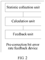
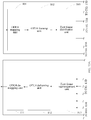
- FIG. 2 shows a structure of the device, including:
- the pre-correction bit error rate of each physical lane may be obtained during FEC decoding and fed back to the optical module.
- the optical module can adjust the receiving parameter of the optical module to reduce the pre-correction bit error rate of each physical lane, thereby improving the quality of each channel of signals demodulated by the optical module.
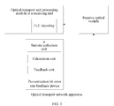
- FIG. 3 shows a structure of the OTN apparatus, including an optical module at a receiving end and a pre-correction bit error rate feedback device shown in FIG. 2 .
- the optical module at the receiving end is configured to demodulate a signal to obtain a signal transmitted on each physical lane, receive a pre-correction bit error rate of each physical lane fed back by the pre-correction bit error rate feedback device, and adjust a receiving parameter of each physical lane according to the pre-correction bit error rate of each physical lane to reduce the pre-correction bit error rate of each physical lane.
- the pre-correction bit error rate feedback device is configured to collect a statistic for an error correction bit rate of data bits of a signal corresponding to each virtual lane during FEC decoding, calculate a pre-correction bit error rate of a physical lane corresponding to each virtual lane according to the error correction bit rate of the data bits of the signal corresponding to each virtual lane, and feed back the pre-correction bit error rate to the optical module at the receiving end.
- the OTN apparatus provided in an embodiment of the present invention is equipped with a pre-correction bit error rate feedback device, so the OTN apparatus can adjust the receiving parameter of the receiving optical module therein according to the pre-correction bit error rate of each physical lane that is fed back by the pre-correction bit error rate feedback device, thereby improving the quality of each channel of signals demodulated by the optical module.
- This embodiment provides a method for improving signal quality.
- the following takes the 100G OTN transmission apparatus and a DP-QPSK demodulation mode as examples for illustration.
- the 100G OTN transmission apparatus includes an OTU (Optical Transport Unit , optical transport unit) processing module and an optical module.
- the OTU processing module includes an OTU processing module at a sending end and an OTU processing module at a receiving end.
- the optical module includes a sending optical module and a receiving optical module.
- the OTU processing module at the sending end may specifically include:
- the sending optical module may specifically include:
- the receiving optical module may specifically include:
- the OTU processing module at the receiving end may specifically include:
- the OTU4 MLD unit 115 at the sending end may specifically distribute a complete OTU4 frame signal onto the 20 virtual lanes according to the following rule:
- the OTU4 frame signal is divided into 16-byte blocks, and the blocks are circularly distributed onto the 20 virtual lanes in a left-to-right and up-to-bottom sequence.
- a start channel for the circular distribution moves down by one channel.
- An FAS (Frame alignment signal) distributed onto each virtual lane carries a number of the virtual lane.
- the first 16 bytes of the OTU4 frame are rotated to a next virtual lane with a interval of 4080 ⁇ 4 bytes (the length of an OTU4 frame), and then the remaining bytes of the frame are distributed in sequence. Therefore, data on each virtual lane corresponds to fixed data in the OTU4 frame. For example, bytes 1-16, bytes 321-336, bytes 641-656, ..., and bytes 16001-16016 correspond to virtual lane 1; and bytes 17-32, bytes 337-352, ..., and bytes 16016-16032 correspond to channel 2.
- the OTU4 MLD unit 115 at the receiving end aligns and rearranges the received signals transmitted on the 20 virtual lanes according to the FAS (Frame Alignment Signal) of a frame header to restore a data format of the original OTU4 frame signal in a rotation manner.
- FAS Frae Alignment Signal
- the method for improving the signal quality is as follows:
- the FEC requires a low output bit error ratio, generally at a level of le-12/1e-15. Therefore, within the error correction capability of the FEC, it can be considered that the number of bits that are corrected per second during the FEC decoding is an error correction bit rate of a signal output by the optical module.
- the FEC decoding unit 113 may obtain a corrected bit location during the FEC decoding, for example, by solving an error location polynomial. By collecting a statistic of the number of the corrected bit locations within the unit time period, the FEC decoding unit may obtain the error correction bit rate of the signal output by the receiving optical module.
- the FEC decoding unit 113 indicates the error correction of the third bit, and therefore the statistic shows that an error occurs in the third bit.
- the error correction bit rate obtained by the decoding unit in each stage during the iterative decoding is obtained.
- the error correction bit rate of the outer code decoding during the first stage iterative decoding, the error correction bite rate of the inner code decoding during the first stage iterative decoding, the error correction bit rate of the outer code decoding during the second stage iterative decoding, and the error correction bit rate of the inner code decoding during the second stage iterative decoding are obtained. The process continues until the error correction bit rates of all the decoding units are obtained.
- the FEC decoding unit 113 may also obtain identification information of the virtual lanes corresponding to the physical lanes restored by the 10:20 DEMUX 116, for example, identifiers of virtual lanes 2, 6, 10, 14, and 18 corresponding to channel I in the X polarization state, and identifiers of virtual lanes 1, 5, 9, 13, and 17 corresponding to channel Q in the X polarization state. Due to data distribution property of multi lane distribution, in each data transmission, data on fixed five virtual lanes is transmitted on the same physical lane.
- the pre-correction bit error rate of the physical lane corresponding to each virtual lane can be determined by determining the error correction bit rate of the virtual lane. Therefore, during the FEC decoding, the error correction bit rates of data bits of a signal corresponding to each of the 20 virtual lanes are calculated respectively, and then according to the error correction bit rates of data bits of the signal corresponding to each virtual lane, the pre-correction bit error rate of the physical lane corresponding to each virtual lane is calculated.
- the error correction bit rates of the data bits of the signals on the virtual lanes identified by the identification information are accumulated to obtain the pre-correction bit error rate of the physical lane corresponding to each virtual lane.
- the receiving optical module adjusts a receiving parameter of each physical lane according to the feedback, and in particular, adjusts a pre-emphasis parameter of each phase (channel I and channel Q) of the QPSK demodulator, a equalizer coefficient, and a threshold value of a decision circuit until the pre-correction bit error rate of each physical lane is minimized and the performance of the receiving optical module is optimal.
- the statistic of the error correction bit rate of the data bits corresponding to each virtual lane may be collected, the pre-correction bit error rate of the physical lanes corresponding to the virtual lanes is calculated through the error correction bit rate and then is fed back to the receiving optical module. Then, the receiving optical module adjusts the receiving parameter accordingly to reduce the pre-correction bit error rate of each physical lane and improve the quality of each channel of signals on each channel demodulated by the optical module. Moveover, the method can be applicable to various FEC solutions.
- the method provided in this embodiment reserves the property of distributing one frame onto multiple optical channels, which facilitates proofing of burst noise on the channel.
- OTU4 used in this embodiment is only an example.
- the present invention is not limited to this, and OTUs of other orders may also be used.
- This embodiment provides another method for improving signal quality, which includes the method, described in Embodiment 1, of calculating a pre-correction bit error rate of each physical lane during FEC decoding.
- a phase difference between channel I and channel of the QPSK demodulator is great, so a bit error of a signal may be great and a bit error rate of the signal may exceed an FEC error correction range.
- the method provided in this embodiment further includes: obtaining BIP-8 (Bit Interleaved Parity 8) information from an OTU4 deframing unit 112 at a receiving end, judging whether the BIP-8 information is correct; if the BIP-8 information is incorrect, feeding back a maximum bit error rate signal to a receiving optical module, where the maximum bit error rate signal indicates that the bit error rate is great and exceeds the FEC error correction range.
- the receiving optical module performs coarse adjustment. For example, the receiving optical module adjusts a pre-emphasis parameter of each phase of the QPSK demodulator, a equalizer coefficient, and a threshold value of a decision circuit until the BIP-8 is correct.
- a statistic of the pre-correction bit error rate of each physical lane is collected and then fed back to the receiving optical module; the receiving optical module adjusts a receiving parameter of each physical lane accordingly until the bit error rate of each physical lane is minimized and the performance of the receiving optical module is optimal.
- the receiving optical module may be instructed by the BIP information to perform coarse adjustment to preliminarily improve the quality of each channel of demodulated signals on each channel, so that the bit error rate of a signal on each channel falls into the FEC error correction range. Then, when the FEC error correction is normally performed, the pre-correction bit error rate of each physical lane in the receiving optical module is obtained. Then, the receiving parameter of each physical lane in the receiving optical module is adjusted accordingly, which further improves the quality of each channel of demodulated signals.
- OTU4 and BIP-8 used in this embodiment are only examples.
- the present invention is not limited thereto, and other OTUs or BIP may also be used.
- This embodiment provides another method for improving signal quality, which includes the method, described in Embodiment 1, of calculating a pre-correction bit error rate of each physical lane during the FEC decoding.
- a phase difference between channel I and channel of a QPSK demodulator is great, so a bit error rate of a signal ma be great and the bit error rate of the signal may exceed an FEC error correction range.
- CRC Cyclic Redundancy Check
- a statistic of the pre-correction bit error rate of each physical lane is collected and then fed back to the receiving optical module; the receiving optical module adjusts a receiving parameter of each physical lane accordingly until the bit error rate of each physical lane is minimized so that the performance of the receiving optical module is optimal.
- the receiving optical module may be instructed by the CRC information to perform coarse adjustment to preliminarily improve the quality of each channel of demodulated signals on each channel, so that the bit error rate of a signal on each channel falls into the FEC error correction range. Then, when the FEC error correction is normally performed, the pre-correction bit error rate of each physical lane in the receiving optical module is obtained. Accordingly, the parameter of each physical lane in the receiving optical module is adjusted, which further improves the quality of each channel of demodulated signals.
- This embodiment provides another method for improving signal quality, which includes the method, described in Embodiment 1, of calculating a pre-correction bit error rate of each physical lane during the FEC decoding.
- the OTU4 MLD unit 115 may not restore the OTU4 frame signal according to the signal transmitted on the virtual lanes.
- the method provided in this embodiment further includes: obtaining a framing failure signal from the OTU4 MLD unit 115 at the receiving end, feeding back the framing failure signal as the maximum bit error rate signal to a receiving optical module.
- the receiving optical module performs coarse adjustment. For example, the receiving optical module adjusts a pre-emphasis parameter of each phase of the QPSK demodulator, a equalizer coefficient, and a threshold value of a decision circuit until the framing failure signal disappears.
- a statistic of the pre-correction bit error rate of each physical lane is collected and then is fed back to the receiving optical module; the receiving optical module adjusts the receiving parameter of each physical lane accordingly until the bit error rate of each physical lane is minimized and the performance of the receiving optical module is optimal.
- the receiving optical module may still be instructed by the obtained framing failure signal to perform coarse adjustment to preliminarily improve the quality of each channel of demodulated signals, so that the OTU4 MLD unit 115 may perform normal framing according to the demodulated signal on the channel. Then, when the FEC error correction is normally performed, the pre-correction bit error rate of each physical lane in the receiving optical module is obtained. Accordingly, the receiving parameter of each physical lane in the receiving optical module is adjusted, which further improves the quality of each channel of demodulated signals.
- This embodiment provides a pre-correction bit error rate feedback device 200, which is applied in an OTN apparatus to obtain a pre-correction bit error rate of each physical lane, and feeds back the obtained pre-correction bit error rate to an optical module in the OTN apparatus so that the optical module can adjust a receiving parameter according to the fed-back pre-correction bit error rate of each physical lane.
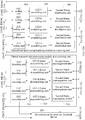
- FIG. 5 shows a structure of the pre-correction bit error rate feedback device 200, including a statistic collection unit 201, a calculation unit 202, and a feedback unit 203.
- the statistic collection unit 201 is configured to collect a statistic of an error correction bit rate of data bits of a signal corresponding to each virtual lane when a FEC decoding unit performs FEC decoding.
- the statistic collection unit 201 obtains a statistic of an error correction bit rate output by a decoding subunit in each stage during the iterative decoding of each stage. For example, error correction bit rates of outer code decoding and inner code decoding during first stage FEC iterative decoding, and error correction bit rates of outer code decoding and inner code decoding during second stage FEC iterative decoding are obtained until the statistic collection unit 201 obtains the error correction bit rates of all the decoding subunits.
- the calculation unit 202 is configured to calculate a pre-correction bit error rate of a physical lane corresponding to each virtual lane according to the error correction bit rate of the data bits of the signal corresponding to each virtual lane.
- a relevant section in Embodiment 1 For the detailed calculation process, reference may be made to a relevant section in Embodiment 1.
- the feedback unit 203 is configured to feed back the pre-correction bit error rate of each physical lane to an optical module so that the optical module adjusts a receiving parameter of each physical lane to reduce the pre-correction bit error rate of each physical lane.
- the pre-correction bit error rate feedback device further includes:
- the feedback unit 203 is further configured to feed back a maximum bit error rate signal to the optical module when the bit interleaved parity check information is incorrect.
- the optical module adjusts the receiving parameter of each physical lane according to the maximum bit error rate signal until the bit interleaved parity check information is correct.
- the optical module may be instructed by the BIP information to perform coarse adjustment to preliminarily improve the quality of each channel of demodulated signals, so that the bit error rate of the signal on each channel falls into the FEC error correction range. Then, when the FEC error correction is normally performed, the pre-correction bit error rate of each physical lane in the optical module is obtained. Thus, the parameter of each physical lane in the optical module is adjusted accordingly, which further improves the quality of each channel of demodulated signals.
- the optical module may be instructed by the CRC information to perform coarse adjustment to preliminarily improve the quality of each channel of demodulated signals, so that the bit error rate of a signal on each channel falls into the FEC error correction range. Then, when the FEC error correction is normally performed, the pre-correction bit error rate of each physical lane in the optical module is obtained. Accordingly, the parameters of each physical lane in the receiving optical module are adjusted, which further improves the quality of each channel of demodulated signals.
- the optical module may still be instructed by obtaining the framing failure signal to perform coarse adjustment to preliminarily improve the quality of each channel of demodulated signals, so that normal framing can be performed according to the demodulated signal on the channel. Then, when the FEC error correction is normally performed, the pre-correction bit error rate of each physical lane in the receiving optical module is obtained. Accordingly, the receiving parameter of each physical lane in the optical module is adjusted, which further improves the quality of each channel of demodulated signals.
- the feedback unit feeds back the pre-correction bit error rate of each physical lane to the optical module.
- the optical module adjusts the receiving parameter of each physical lane.
- the receiving optical module in the optical module adjusts the receiving parameter of each physical lane.
- the statistic of the error correction bit rate of the data bits corresponding to each virtual lane can be collected, and the pre-correction bit error rate of the physical lanes corresponding to the virtual lanes is calculated through the error correction bit rate and fed back to the optical module. Then, the optical module can adjust the receiving parameter of each physical lane accordingly to reduce the pre-correction bit error rate of each physical lane, which improves the quality of the signal corresponding to each physical lane in the optical module.
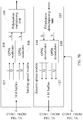
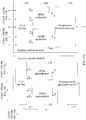
- This embodiment provides an OTN apparatus, as shown in FIG. 6 .
- the OTN apparatus provided in this embodiment is additionally installed with a pre-correction bit error rate feedback device 200 as described in Embodiment 5.
- the OTN apparatus provided in this embodiment may improve signal quality.
- the OTN apparatus includes: an OTU processing module, an optical module, and a pre-correction bit error rate feedback device 200.
- the OTU processing module includes an OTU processing module at a sending end and an OTU processing module at a receiving end.
- the optical module includes a sending optical module and a receiving optical module.
- the OTU processing module at the sending end may specifically include an ODU4 mapping unit 101, an OTU4 framing unit 102, an FEC coding unit 103, an OTU4 scrambling unit 104, an OTU4 MLD unit 105, and a 20:10 MUX 106.
- the OTU processing module at the receiving end may specifically include an ODU4 demapping unit 111, an OTU4 deframing unit 112, an FEC decoding unit 113, an OTU4 descrambling unit 114, an OTU4 MLD unit 115, and a 10:20 DEMUX 116.
- the sending optical module may specifically include a 10:4 SerDes 107, two QPSK demodulators 108, and a polarization multiplexing unit 109.
- the receiving optical module may specifically include a 4:10 SerDes 117, two QPSK demodulators 118, and a polarization demultiplexing unit 119.
- the pre-correction bit error rate feedback device 200 collects a statistic of an error correction bit rate of data bits of a signal corresponding to each virtual lane, calculates a pre-correction bit error rate of a physical lane corresponding to each virtual lane according to the error correction bit rate of the data bits of the signal corresponding to each virtual lane, and feeds back the pre-correction bit error rate to the receiving optical module.
- the pre-correction bit error rate feedback device 200 calculates the pre-correction bit error rate of the physical lane corresponding to the virtual lanes according to the error correction bit rates of the data bits of the signal corresponding to each virtual lane. To be specific, the pre-correction bit error rate feedback device 200 obtains identification information of the virtual lanes, corresponding to the physical lanes, that are restored by the 10:20 DEMUX 116, accumulates the error correction bit rates of the virtual lanes identified by the identification information to obtain the pre-correction bit error rate of the physical lane corresponding to each virtual lane.
- the identification information of each virtual lane can be obtained during the FEC decoding only according to a channel distribution rule applied by the OTU4 MLD unit 105, and it is not required to obtain the identification information of the virtual lane from the 10:20 DEMUX 116.
- the error correction bit rates of the data bits of the signals on all virtual lanes corresponding to each physical lane are accumulated. This accumulation may be carried out for data within a frame period. In other embodiments, this accumulation may be, however, carried out for data within a period shorter than the frame period, and also may be carried out for the data within a period longer than the frame period.
- the error correction bit rates of the virtual lanes corresponding to each physical lane may be averaged to obtain the pre-correction bit error rate of each physical lane.
- the receiving optical module adjusts the receiving parameter of each physical lane according to the pre-correction bit error rate of each physical lane fed back by the pre-correction bit error rate feedback device 200.
- a pre-emphasis parameter of each phase (channel I and channel Q) of the QPSK demodulator, a equalizer coefficient, and a threshold value of a decision circuit are adjusted so that the bit error rate of each physical lane is minimized and the performance of the receiving optical module is optimal.
- the pre-correction bit error rate feedback device 200 may also obtain BIP-8 information from the OTU4 deframing unit 112, and judge whether the BIP-8 information is correct. If the BIP-8 information is incorrect, the pre-correction bit error rate feedback device 200 feeds back a maximum bit error rate signal to the receiving optical module, where the maximum bit error rate signal indicates that the bit error rate is great and exceeds an FEC error correction range. According to the maximum bit error rate signal, the receiving optical module performs coarse adjustment. For example, the receiving optical module adjusts the pre-emphasis parameter of each phase (channel I and channel Q) of the QPSK demodulator, the equalizer coefficient, and the threshold value of the decision circuit until the BIP-8 information is correct.
- the pre-correction bit error rate feedback device 200 may also obtain CRC information when the FEC decoding unit 113 performs the FEC decoding, and judge whether the CRC information is correct. If the CRC information is incorrect, the pre-correction bit error rate feedback device 200 feeds back a maximum bit error rate signal to the receiving optical module, where the maximum bit error rate signal indicates that the bit error rate is great and exceeds the FEC error correction range. According to the maximum bit error rate signal, the receiving optical module performs coarse adjustment. For example, the receiving optical module adjusts the pre-emphasis parameter of each phase of the QPSK demodulator, the equalizer coefficient, and the threshold vale of the decision circuit until the CRC information is correct.
- the pre-correction bit error rate feedback device 200 may also obtain a framing failure signal from the OTU4 MLD unit 115 and feeds back the framing failure signal as a maximum bit error rate signal to the receiving optical module.
- the receiving optical module performs coarse adjustment. For example, the receiving optical module adjusts the pre-emphasis parameter of each phase of the QPSK demodulator, the equalizer coefficient, and the threshold value of the decision circuit until the OTU4 MLD unit 115 can perform framing normally.
- the OTN apparatus provided in this embodiment is installed with a pre-correction bit error rate feedback device. Therefore, the error correction bit rate of the data bits of the signal corresponding to each virtual lane may be calculated, and the pre-correction bit error rate of the physical lane corresponding to each virtual lane can be calculated according to the error correction bit rate of the data bits of the signal corresponding to each virtual lane.
- the calculated pre-correction bit error rate of each physical lane is fed back to the receiving optical module.
- the receiving optical module can adjust the receiving parameter of each physical lane accordingly to reduce the pre-correction bit error rate of each physical lane, which improves the quality of each channel of signals demodulated by the receiving optical module.
- the maximum bit error rate signal may be obtained through the pre-correction bit error rate feedback device, and then the receiving parameter of each physical in the receiving optical module is adjusted coarsely according to the maximum bit error rate signal.
- the pre-correction bit error rate of each physical lane is obtained through the feedback device for feeding back the pre-correction bit error rate, and then the receiving parameter of each physical lane in the receiving optical module is adjusted, which further improves the quality of each channel of signals demodulated by the receiving optical module.
- the pre-correction bit error rate feedback device 200 and the FEC decoding unit 113 are discrete. In other embodiments, the pre-correction bit error rate feedback device 200 may also be integrated into the FEC decoding unit 113, or a part of functions of the pre-correction bit error rate feedback device 200 is integrated into the FEC decoding unit 113. It should be noted that, in the present invention, for the convenience of description, the optical module is divided into a sending optical module and a receiving optical module according to functions of sending and receiving. In other scenarios, the optical module can perform both transmitting and receiving, so an entire optical module rather than the sending optical module and receiving optical module is visible, which also falls within the protection scope of the present invention.
- This embodiment provides another OTN apparatus, a structure of which is shown in FIG. 7 .
- the OTN apparatus provided in this embodiment replaces the OTU4 MLD unit 105 and the OTU4 MLD unit 115 in the OTN apparatus in Embodiment 6 and FIG. 6 with a frame distribution unit 305 at a frame distribution interface in a sending part and a frame rearrangement unit 315 in a receiving part respectively, and other parts are the same.
- the frame distribution unit 305 is configured to distribute the OTU4 frame scrambled by the OTU4 scrambling unit 104 onto 20 virtual lanes in the unit of frame.
- the frame distribution unit 305 distributes the OTU4 frame onto a corresponding virtual lane among the 20 virtual lanes according to a value of the third OA2 byte of an FAS in each OTU4 frame.
- a format of the FAS is OA1OA1OA1OA2OA2OA2, and the third OA2 is used in this embodiment.
- the process of distributing the OTU4 frame onto the corresponding virtual lane among the 20 virtual lanes according to the value (ranging from 0 to 239) of the third OA2 byte of the FAS in each OTU4 frame may specifically include as follows. For each OTU4 frame, modulo 20 residue operation is performed on the third OA2 of the FAS. The obtained residue is a number of the virtual lane. Then, the OTU4 frame is distributed onto the virtual lane identified by the number of the virtual lane.
- the 20:10 MUX 106 multiplexes the signals transmitted on the 20 virtual lanes into 10 channels of signals.
- the multiplexing rule is: multiplexing signal bits on every two virtual lanes into a signal on one channel.
- the 10:4 SerDes 107 performs 10:4 multiplexing on the 10 channels of signals multiplexed by the 20:10 MUX 106 to multiplex the 10 channels of signals onto four physical lanes.
- the four physical lanes are channel I in an X polarization state, channel Q in the X polarization state, channel I in a Y polarization, and channel Q in the Y polarization state.
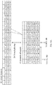
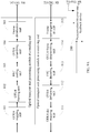
- FIG. 8 shows the whole process for the frame distribution unit 305 to distribute the scrambled OTU4 frame onto 20 virtual lanes and for the 10:4 SerDes 107 to obtain signals transmitted on the four physical lanes.
- i-1, i8-1, i16-5, i5-1, and il3-1 in the first column from the left in the table in the bottom of FIG. 8 correspond to frame 0, frame 8, frame 16, frame 5, frame 13 respectively;
- i-2, i8-2, i16-2, and i5-2 correspond to frame 0, frame 8, frame 16, frame 5, and frame 13 respectively.
- the rest may be deducted by analogy. That is, frame 0, frame 8, frame 16, frame 5, and frame 13 are on the physical lane in the first column from the left.
- FIG. 5 it can be seen from FIG. 5 that, these five frames do not appear on the physical lanes corresponding to other three columns. That is, the bits of these frames are distributed onto this physical lane. Accordingly, the data of each OTU4 frame is transmitted on one physical lane.
- the 4:10 SerDes 117 performs 4:10 demultiplexing on signals on the four physical lanes obtained by two QPSK demodulators to obtain 10 channels of signals.
- the 10:20 DEMUX 116 performs 1:2 bit demultiplexing on the 10 channels of signals to restore the signals transmitted on the 20 virtual lanes.
- the frame rearrangement unit 315 performs frame alignment and rearrangement on the signals on the 20 virtual lanes restored by the 10:20 DEMUX 116 to restore the OTU4 frame signal.
- the frame alignment and rearrangement performed by the frame rearrangement unit 315 are performed in the unit of frame.
- the pre-correction bit error rate feedback device 200 feeds back the obtained pre-correction bit error rate of each physical lane to the receiving optical module as a feedback signal so that the receiving optical module adjusts the receiving parameter of each physical lane accordingly, thereby improving the quality of each channel of signals demodulated by the receiving optical module and improving the receiving performance of the receiving optical module.
- the pre-correction bit error rate feedback device 200 For the structure and working process of the pre-correction bit error rate feedback device 200, reference may be made to relevant description in Embodiment 5. The details will not be described here again.
- the OTU4 framing is implemented by the frame rearrangement unit 315.
- the pre-correction bit error rate feedback device in this embodiment specifically obtains a framing failure signal from the frame rearrangement unit 315.
- the OTN provided in this embodiment is installed with a pre-correction bit error rate feedback device. Therefore, the receiving parameter of each physical lane in the receiving optical module can be adjusted according to the pre-correction bit error rate of each physical lane that is fed back by the pre-correction bit error rate feedback device, which improves the quality of each channel of signals demodulated by the receiving optical module.
- the OTN apparatus distributes the scrambled OTU4 frame on each virtual lane in the unit of frame during the data processing by the OTU at the sending end, data transmitted on each physical lane is data transmitted on fixed virtual lanes, so that data of each frame is modulated to a carrier only through one physical lane for transmission, which simplifies data processing by the OTU at the receiving end, especially data processing by the pre-correction bit error rate feedback device 200.
- the pre-correction bit error rate feedback device 200 may not need to obtain the identification information of the virtual lanes corresponding to each physical lane from the 10:20 DEMUX 116 in real time.
- the identification information of the virtual lanes and the corresponding information between the virtual lane and the physical lane may be configured manually in the pre-correction bit error rate feedback device 200 or in the system information statically.
- the virtual lane and physical lane corresponding to the frame may be judged according to the value of the third OA2 byte of the FAS in the OTU4 frame. It can be seen from FIG. 8 that, interleaved bits of five frames are carried on each physical lane. In the case that the burst consecutive bit error codes are distributed onto the neighboring five OTU4 frames, the OTN apparatus provided in this embodiment has powerful capability of FEC burst consecutive bit error correction.
- This embodiment provides an OTN apparatus, a structure of which is shown in FIG. 9 .
- the OTN apparatus in the embodiment replaces the 20:10 MUX 106, 10:4 SerDes 107, 4:10 SerDes 117, and 10:20 DEMUX 116 in the OTN apparatus shown in Embodiment 7 and FIG. 7 with a 20:4 SerDes 407 and a 4:20 SerDes 417, and other parts are the same.
- the 20:4 SerDes 407 multiplexes the signals transmitted on the 20 virtual lanes obtained by the frame distribution unit 305 onto four physical lanes.
- the multiplexing rule is: multiplexing bits of signals transmitted on every five virtual lanes onto one physical lane, for example, multiplexing bits of signals transmitted on virtual lanes 0, 4, 8, 12, 16 onto one physical lane.
- FIG. 10 For the specific multiplexing process, reference may be made to FIG. 10 .
- the 4:20 SerDes 417 demultiplexes the signals transmitted on four physical lanes to restore the signals transmitted on the 20 virtual lanes.
- the demultiplexing process is reverse to the multiplexing process in the 20:4 SerDes 407.
- the OTN apparatus in this embodiment simplifies the multiplexing and demultiplexing processes and improves the processing efficiency of the OTN apparatus by using the 20:4 SerDes 407 and the 4:20 SerDes 417.
- the 20:4 SerDes 407 and the 4:20 SerDes 417 are installed in the sending optical module and the receiving optical module respectively. It can be understood that the 20:4 SerDes 407 and the 4:20 SerDes 417 may also be installed in the OTU processing module at the sending end and the OTU processing module at the receiving end respectively.
- the OTU4 framing is implemented by the frame rearrangement unit 315.
- the pre-correction bit error rate feedback device in this embodiment obtains a framing failure signal from the frame rearrangement unit 315.
- the functions implemented by the 20:10 MUX 106 and the 10:4 SerDes 107 in cooperation are similar to the functions implemented by the 20:4 SerDes 407 in this embodiment:
- the signals transmitted on the 20 virtual lanes are multiplexed onto four physical lanes.
- the 20:10 MUX 106 and the 10:4 SerDes 107 are integrated into a multiplexing module to implement the multiplexing function.
- the signals transmitted on the 20 virtual lanes are multiplexed onto four physical lanes.
- the 20:4 SerDes 407 in this embodiment may also be designed to a multiplexing module separately.
- the 4:10 SerDes 117 and the 10:20 DEMUX 116 in Embodiment 7 are integrated into a demultiplexing module.
- the 4:20 SerDes 417 in this embodiment may also be designed to a demultiplexing module separately.
- This embodiment further provides an OTN apparatus, a structure of which is shown in FIG. 11 .
- the OTN apparatus in this embodiment replaces the FEC decoding unit 103, the OTU4 scrambling unit 104, and the frame distribution unit 305 in the OTN apparatus described in Embodiment 7 and FIG. 7 with a first frame distribution unit 503, five parallel FEC decoding units 504, five parallel OTU4 scrambling units 505, and five parallel second frame distribution units 506.
- the OTN apparatus in this embodiment replaces the FEC decoding unit 113, the OTU4 descrambling unit 114, and the frame rearrangement unit 315 in the OTN apparatus described in Embodiment 7 and FIG.
- the first frame distribution unit 503 distributes a serial OTU4 frame signal obtained by the OTU4 framing unit 102 into five channels of parallel OTU4 frame signals in the unit of frame.
- the distribution is performed according to a value of the third OA2 byte of the FAS in the OTU4 frame.
- An operation of calculating a residue for the value of the OA2 byte modulo 5 is performed. If a residue for a value of the third OA2 bytes of frames having modulo 5 is 0, the frames are distributed onto the same channel. For example, the OTU4 frames with the third OA2 bytes 0, 5, 10, and 15 are distributed onto the same channel. In the case of other residues, the frames are also distributed in this manner.
- the five parallel FEC decoding units 504 perform FEC coding on the five channels of parallel OTU4 frame signals respectively.
- the five parallel OTU4 scrambling units 505 scramble the five channels of parallel FEC-coded OTU4 frame signals respectively.
- the five second frame distribution units 506 distribute the five channels of parallel scrambled OTU4 frame signals onto 20 virtual lanes.
- the distribution rule may specifically be: distributing the scrambled signal on each channel onto four virtual lanes in turn in unit of frame.
- the five parallel second frame rearrangement units 516 performs frame alignment and rearrangement on the signals transmitted on the 20 virtual lanes restored by the 10:20 DEMUX 116 to restore the five channels of parallel signals.
- the five parallel OTU4 descrambling units 515 descramble the five channels of parallel restored signals respectively.
- the five parallel FEC decoding units 514 perform FEC decoding on the five channels of parallel descrambled signals respectively.
- the first frame rearrangement unit 513 performs framing and rearrangement on the five channels of parallel signals to obtain one channel of serial OTU4 frames through combination, and then sends the frames to the OTU4 deframing unit for subsequent processing.
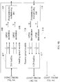
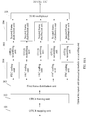
- FIG. 12A shows the frame distribution process performed by the first frame distribution unit 503 and the five second frame distribution units 506.
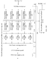
- FIG. 12B shows the frame rearrangement process performed by the first frame rearrangement unit.
- the pre-correction bit error rate feedback device 200 is specifically configured to collect a statistic of an error correction bit rate of data bits of a signal corresponding to each virtual lane when each FEC decoding unit 514 performs the FEC decoding, calculate a pre-correction bit error rate of a physical lane corresponding to each virtual lane according to the error correction bit rate of the data bits of the signal corresponding to each virtual lane, and feed back the calculated pre-correction bit error rate of each physical lane to the receiving optical module.
- the receiving optical module adjusts the receiving parameter of each physical lane according to the fed back pre-correction bit error rate to reduce the pre-correction bit error rate of each physical lane.
- the pre-correction bit error rate feedback device 200 obtains the framing failure signal from the five parallel second frame rearrangement units 516.
- the framing failure signal may be obtained from one or all of the five parallel frame rearrangement units 516, which is not limited in the present application.
- the OTN apparatus converts one channel of high-speed serial OTU4 signals into five channels of low-speed parallel OTU4 signals.
- the subsequent processing (such as FEC coding and OTU4 scrambling) is based on the five channels of low-speed parallel OTU4 signals. Therefore, requirements for the performance of components for implementing the processing are decreased, and the implementation difficulty of the OTN apparatus is decreased.
- FIG. 13 A structure of an OTN apparatus provided in another embodiment is shown in FIG. 13 .
- the 20:10 MUX 106, 10:4 SerDes 107, 4:10 SerDes 117, and 10:20 DEMUX 116 are replaced with the 20:4 SerDes 407 and 4:20 SerDes 417 respectively.
- the 20:4 SerDes 407 and 4:20 SerDes 417 For the detailed processing of the 20:4 SerDes 407 and 4:20 SerDes 417, reference may be made to relevant description in Embodiment 8.
- the serial OTU4 frame signal obtained by the OTU4 framing unit 102 are distributed into five channels of the parallel OTU4 signals in the unit of frame; each second frame distribution unit 506 distributes one channel of the scrambled OTU4 frame signal of the five channels of scrambled OTU4 frame signals onto four virtual lanes in the unit of frame, and then the signals transmitted on the 20 virtual lanes are multiplexed onto four physical lanes.
- the distribution method by the first frame distribution unit 503 and the second frame distribution unit 506 is not limited to the distribution method provided in this embodiment.
- the first frame distribution unit 503 distributes the serial OTU4 frame signal obtained by the OTU4 framing unit 102 into L parallel channels of OTU4 frame signals; each second frame distribution unit 506 distributes one channel of scrambled OTU4 frame signals in the L channels of scrambled OTU4 frame signals onto M virtual lanes in the unit of frame, and then multiplexes the signals transmitted on the L ⁇ M virtual lanes onto N physical lanes, where L, M, and N are integers and greater than 1.
- This embodiment provides another OTN apparatus, a structure of which is shown in FIG. 14 .
- the OTN apparatus in this embodiment differs from the OTN apparatus described in Embodiment 7 in that the sending optical module includes an QPSK modulator 108 and a 10:2 SerDes 607 and the receiving optical module includes an QPSK demodulator 118 and a 2:10 SerDes 617.
- the 10:2 SerDes 607 performs 10:2 multiplexing on the 10 channels of signals obtained by the 20:10 MUX 106 to multiplex the signals onto two physical lanes (channel I and channel Q).
- the QPSK modulator performs the QPSK modulation on the optical carrier according to data transmitted on the two physical lanes (channel I and channel Q) to obtain a QPSK modulated signal.
- the 10:2 multiplexing performed by the 10:2 SerDes 607 is similar to the 10:4 multiplexing in other embodiments. The details will not be described here again.
- the QPSK demodulator 118 performs the QPSK demodulation on the QPSK modulated signal sent by the OTN apparatus at the peer end to restore the data transmitted on the two physical lanes (channel I and channel Q).
- the 2:10 SerDes 617 performs the 2:10 demultiplexing on the data transmitted on the two physical lanes to obtain the 10 channels of signals.
- the 2:10 demultiplexing performed by the 2:10 SerDes 607 is similar to the 4:10 demultiplexing in other embodiments, and is reverse to the 10:2 multiplexing performed by the 10:2 SerDes 607. The details will not be described here again.
- the OTN apparatus provided in this embodiment simplifies the signal processing in the sending optical module and the receiving optical module.
- the 20:10 MUX 106 and 10:2 SerDes 607 in this embodiment are replaced with the 20:2 SerDes
- the 2:10 SerDes and the 10:20 DEMUX 116 in this embodiment are replaced with the 2:20 SerDes.
- the FEC coding unit 103, the OTU4 scrambling unit 104, and the frame distribution unit 305 in the OTU processing module at the sending end in this embodiment are replaced with a first frame distribution unit, five parallel FEC coding units, five OTU4 scrambling units, and five parallel second frame distribution units;
- the FEC decoding unit 113, the OTU4 descrambling unit 114, and the frame arrangement unit 315 in the OTU processing module at the receiving end in this embodiment are replaced with a first frame arrangement unit, five parallel FEC decoding units, five OTU4 descrambling units, and five parallel second frame arrangement units.
- a part of OTU processing is directed to the parallel signals, requirements for the performance of components for implementing the processing are decreased and the implementation difficulty of the OTN apparatus is decreased.
- the preceding embodiments are all directed to the OTU4 frame. It can be understood that the present invention is also applicable to OTUs with other orders. According to the preceding embodiments, although the modulator in sending optical module is the QPSK modulator and the demodulator in the receiving optical module is the QPSK demodulator, the embodiments of the present invention are also applicable if the modulator in the sending optical module is a DQPSK modulator and the demodulator in the receiving optical module is a DQPSK demodulator.
- the embodiments of the present invention are mainly applied in the field of communications technologies. With the development of the network technology, the embodiments of the present invention are likely to be applied in other scenarios or other similar technical fields.
- the software product may be stored in a readable storage medium, such as a floppy disk, a hard disk, and an optical disc of a computer, and includes a number of instructions that enable an apparatus to execute the methods provided in the embodiments of the present invention.
Landscapes
- Engineering & Computer Science (AREA)
- Computer Networks & Wireless Communication (AREA)
- Signal Processing (AREA)
- Quality & Reliability (AREA)
- Optical Communication System (AREA)
- Detection And Prevention Of Errors In Transmission (AREA)
Claims (3)
- Verfahren zum Verbessern einer Signalqualität, Folgendes umfassend:an einem Sendeende, Verteilen eines verwürfelten optischen Transporteinheitsrahmensignals auf mehrere Signale, die auf entsprechenden virtuellen Spuren in einer Einheit eines Rahmens übertragen werden, und Multiplexen der Signale, die auf den virtuellen Spuren übertragen werden, um Signale zu erhalten, die auf entsprechenden physischen Spuren übertragen werden;an einem Empfangsende, Demultiplexieren der Signale, die auf den physischen Spuren übertragen werden, um die Signale zu erhalten, die auf jeder entsprechenden virtuellen Spur übertragen werden, und Umordnen der Signale, die auf den virtuellen Spuren übertragen werden, um das optische Transporteinheitsrahmensignal wiederherzustellen;Sammeln (S1) einer Statistik einer Fehlerkorrekturbitrate von Datenbits eines Signals, das jeder virtuellen Spur während einer Decodierung einer Fehlerkorrektur bei Weiterleitung (forward error correction - FEC) entspricht;Berechnen (S2) einer Vorkorrekturbitfehlerrate jeder physischen Spur, die jeder virtuellen Spur entspricht, gemäß der Fehlerkorrekturbitrate der Datenbits des Signals, das jeder virtuellen Spur entspricht;Rückkoppeln (S3) der Vorkorrekturbitfehlerrate jeder physischen Spur an ein optisches Modul, wobei sich das optische Modul an dem Empfangsende befindet; undAnpassen (S4) eines Empfangsparameters jeder physischen Spur durch das optische Modul, um die Vorkorrekturbitfehlerrate jeder physischen Spur zu verringern.
- Optisches Transportnetzwerksystem, an einem Sendeende Folgendes umfassend:eine Rahmenverteilungseinheit, die konfiguriert ist, um ein verwürfeltes optisches Transporteinheitsrahmensignal auf mehrere Signale zu verteilen, die auf entsprechenden virtuellen Spuren in der Einheit des Rahmens übertragen werden; ein Multiplexmodul, das konfiguriert ist, um die Signale zu multiplexen, die auf den virtuellen Spuren übertragen werden, um Signale zu erhalten, die auf entsprechenden physischen Spuren übertragen werden;an einem Empfangsende:ein Demultiplexmodul, das konfiguriert ist, um die Signale zu demultiplexen, die auf den physischen Spuren übertragen werden, um die Signale zu erhalten, die auf jeder entsprechenden virtuellen Spur übertragen werden;eine Rahmenumordnungseinheit, die konfiguriert ist, um eine Rahmenumordnung auf den Signalen durchzuführen, die auf den virtuellen Spuren übertragen werden und durch das Demultiplexmodul erhalten werden, um das optische Transporteinheitsrahmensignal wiederherzustellen; undeine Vorkorrekturbitfehlerratenrückkopplungsvorrichtung (200), die konfiguriert ist, um eine Statistik einer Fehlerkorrekturbitrate von Datenbits eines Signals zu sammeln, das jeder virtuellen Spur während der FEC-Decodierung entspricht, um eine Vorkorrekturbitfehlerrate jeder physischen Spur, die jeder virtuellen Spur entspricht, gemäß der Fehlerkorrekturbitrate der Datenbits des Signals, das jeder virtuellen Spur entspricht, zu berechnen, und um die Vorkorrekturbitfehlerrate an ein optisches Modul an dem Empfangsende rückzukoppeln;das optische Modul an dem Empfangsende, das konfiguriert ist, um eine Vorkorrekturbitfehlerrate jeder physischen Spur, die durch die Vorkorrekturbitfehlerratenrückkopplungsvorrichtung rückgekoppelt wird, zu empfangen und um einen Empfangsparameter jeder physischen Spur gemäß der Vorkorrekturbitfehlerrate jeder physischen Spur anzupassen, um die Vorkorrekturbitfehlerrate jeder physischen Spur zu verringern.
- System nach Anspruch 2, wobei die Vorkorrekturbitfehlerratenrückkopplungsvorrichtung Folgendes umfasst:eine Statistiksammlungseinheit (201), die konfiguriert ist, um die Statistik einer Fehlerkorrekturbitrate von Datenbits eines Signals, das jeder virtuellen Spur entspricht, während der FEC-Decodierung zu sammeln;eine Berechnungseinheit (202), die konfiguriert ist, um die Vorkorrekturbitfehlerrate der physischen Spur, die jeder virtuellen Spur entspricht, gemäß der Fehlerkorrekturbitrate der Datenbits des Signals auf jeder virtuellen Spur zu berechnen; undeine Rückkopplungseinheit (203), die konfiguriert ist, um die Vorkorrekturbitfehlerrate jeder physischen Spur an das optische Modul derart rückzukoppeln, dass das optische Modul den Empfangsparameter jeder physischen Spur anpasst, um die Vorkorrekturbitfehlerrate jeder physischen Spur zu verringern.
Applications Claiming Priority (1)
| Application Number | Priority Date | Filing Date | Title |
|---|---|---|---|
| PCT/CN2009/073560 WO2011022886A1 (zh) | 2009-08-27 | 2009-08-27 | 一种改善信号质量的方法、装置及设备 |
Publications (3)
| Publication Number | Publication Date |
|---|---|
| EP2461623A1 EP2461623A1 (de) | 2012-06-06 |
| EP2461623A4 EP2461623A4 (de) | 2012-10-24 |
| EP2461623B1 true EP2461623B1 (de) | 2020-02-26 |
Family
ID=43627152
Family Applications (1)
| Application Number | Title | Priority Date | Filing Date |
|---|---|---|---|
| EP09848618.6A Active EP2461623B1 (de) | 2009-08-27 | 2009-08-27 | Verfahren und system zur verbesserung der signalqualität |
Country Status (3)
| Country | Link |
|---|---|
| EP (1) | EP2461623B1 (de) |
| CN (1) | CN102577490B (de) |
| WO (1) | WO2011022886A1 (de) |
Cited By (1)
| Publication number | Priority date | Publication date | Assignee | Title |
|---|---|---|---|---|
| WO2025106744A1 (en) * | 2023-11-14 | 2025-05-22 | Marvell Asia Pte Ltd | Monitoring fec information in multi-chip environment |
Families Citing this family (14)
| Publication number | Priority date | Publication date | Assignee | Title |
|---|---|---|---|---|
| EP2999152A4 (de) * | 2013-05-17 | 2017-03-22 | Huawei Technologies Co., Ltd. | Datenverarbeitungsverfahren und zugehörige vorrichtung für fec-codierung und -decodierung |
| CN104426631B (zh) * | 2013-09-06 | 2018-03-06 | 华为技术有限公司 | 对数据进行处理的方法及装置 |
| EP3107234B1 (de) * | 2014-02-17 | 2018-03-28 | Huawei Technologies Co., Ltd. | Verfahren, vorrichtung und system zur übertragung eines signals in einem optimalen übertragungsnetzwerk |
| CN103929170B (zh) * | 2014-04-09 | 2017-06-06 | 中航海信光电技术有限公司 | 一种多通道并行光模块启动方法 |
| CN105406937B (zh) * | 2014-09-12 | 2020-03-03 | 中兴通讯股份有限公司 | 定帧方法及装置 |
| CN108449219B (zh) * | 2018-06-21 | 2021-05-14 | 武汉意谷光电科技有限公司 | 一种光模块自动优化配置的方法及系统 |
| US10644792B2 (en) * | 2018-07-16 | 2020-05-05 | Juniper Networks, Inc. | Methods and apparatus for adaptively detecting signal degradation in an optical communication system using the pre-forward error correction bit error rate |
| CN110930910B (zh) * | 2019-12-02 | 2021-07-06 | Tcl华星光电技术有限公司 | 一种显示面板中信号的处理方法及装置 |
| US11043154B1 (en) | 2019-12-02 | 2021-06-22 | Tcl China Star Optoelectronics Technology Co., Ltd. | Signal processing method for display panel and device using same |
| CN113381840B (zh) | 2020-03-10 | 2022-06-10 | 华为技术有限公司 | 一种信息处理方法及装置 |
| CN113783602B (zh) * | 2021-08-31 | 2023-07-11 | 西南电子技术研究所(中国电子科技集团公司第十研究所) | 卫星通信数据质量提升装置 |
| CN118300758B (zh) * | 2024-06-03 | 2024-08-23 | 中国科学院空天信息创新研究院 | 遥感卫星数传误码率计算方法 |
| CN118802652B (zh) * | 2024-09-10 | 2024-12-20 | 芯潮流(珠海)科技有限公司 | 高精度误码率统计的方法和接收装置 |
| CN120281437B (zh) * | 2025-06-06 | 2025-10-14 | 中星联华科技(北京)股份有限公司 | 一种并行的误码率检测方法、装置、介质及产品 |
Family Cites Families (7)
| Publication number | Priority date | Publication date | Assignee | Title |
|---|---|---|---|---|
| CN1135867C (zh) * | 1998-06-30 | 2004-01-21 | 三菱电机株式会社 | 移动通信终端 |
| US6742154B1 (en) * | 2000-05-25 | 2004-05-25 | Ciena Corporation | Forward error correction codes for digital optical network optimization |
| US20020178417A1 (en) * | 2001-05-22 | 2002-11-28 | Jacob John M. | Communication channel optimization using forward error correction statistics |
| US6829741B1 (en) * | 2001-07-27 | 2004-12-07 | Centillium Communications, Inc. | Forward error correction (FEC) based on SONET/SDH framing |
| JP4620642B2 (ja) * | 2006-07-31 | 2011-01-26 | 富士通株式会社 | 多値変調受信装置 |
| US20090060497A1 (en) * | 2007-08-30 | 2009-03-05 | Way Winston I | Feedback Controlled Locking of Optical Channel Signals in Optical Receivers in Wavelength Division Multiplexed (WDM) Communication Systems |
| CN101369853A (zh) * | 2008-09-26 | 2009-02-18 | 中兴通讯股份有限公司 | 一种优化波长通道色散补偿的方法及其装置 |
-
2009
- 2009-08-27 WO PCT/CN2009/073560 patent/WO2011022886A1/zh not_active Ceased
- 2009-08-27 CN CN200980121543.6A patent/CN102577490B/zh active Active
- 2009-08-27 EP EP09848618.6A patent/EP2461623B1/de active Active
Non-Patent Citations (1)
| Title |
|---|
| None * |
Cited By (1)
| Publication number | Priority date | Publication date | Assignee | Title |
|---|---|---|---|---|
| WO2025106744A1 (en) * | 2023-11-14 | 2025-05-22 | Marvell Asia Pte Ltd | Monitoring fec information in multi-chip environment |
Also Published As
| Publication number | Publication date |
|---|---|
| WO2011022886A1 (zh) | 2011-03-03 |
| EP2461623A1 (de) | 2012-06-06 |
| EP2461623A4 (de) | 2012-10-24 |
| CN102577490A (zh) | 2012-07-11 |
| CN102577490B (zh) | 2014-03-05 |
Similar Documents
| Publication | Publication Date | Title |
|---|---|---|
| EP2461623B1 (de) | Verfahren und system zur verbesserung der signalqualität | |
| US7970008B2 (en) | Multiplexing transmission system and multiplexing transmission method | |
| US20200014610A1 (en) | Ethernet signal transport method and scheduling method, and apparatus and system thereof | |
| EP2975858B1 (de) | Verfahren zur datenverarbeitung im ethernet, chip mit einer physikalischen schicht und ethernetvorrichtung | |
| US8045863B2 (en) | Byte-interleaving systems and methods for 100G optical transport enabling multi-level optical transmission | |
| US8705974B2 (en) | Optical transmission system and optical transmission method | |
| US9231721B1 (en) | System and method for scaling total client capacity with a standard-compliant optical transport network (OTN) | |
| EP1722493B1 (de) | Verfahren, geräte und system zur optischen kommunikation | |
| US7555008B2 (en) | Method and apparatus for providing a Gigabit Ethernet circuit pack | |
| JP4870742B2 (ja) | 光伝送装置 | |
| CN104350716A (zh) | 多通道传送装置以及多通道传送方法 | |
| US9755756B2 (en) | Transmission device, transmission system, and transmission method | |
| JP3947417B2 (ja) | 波長分割多重システム | |
| US8125979B2 (en) | Multi-channel optical transport network training signal wrapper | |
| US6847655B2 (en) | Method and apparatus for transmitting/receiving high order digital signals over two RF carriers in a radio regeneration section | |
| US8160057B2 (en) | Multi-channel optical transport network training signal | |
| CN1197367C (zh) | 一种帧的生成方法及视频数据的发送/接收装置和方法 | |
| CN1229311A (zh) | 传输容量可配置的无线传输系统及相应的发射机和接收机 | |
| JP2009521883A (ja) | オーバーヘッド情報を送信するための方法及び装置 |
Legal Events
| Date | Code | Title | Description |
|---|---|---|---|
| PUAI | Public reference made under article 153(3) epc to a published international application that has entered the european phase |
Free format text: ORIGINAL CODE: 0009012 |
|
| 17P | Request for examination filed |
Effective date: 20120301 |
|
| AK | Designated contracting states |
Kind code of ref document: A1 Designated state(s): AT BE BG CH CY CZ DE DK EE ES FI FR GB GR HR HU IE IS IT LI LT LU LV MC MK MT NL NO PL PT RO SE SI SK SM TR |
|
| A4 | Supplementary search report drawn up and despatched |
Effective date: 20120926 |
|
| RIC1 | Information provided on ipc code assigned before grant |
Ipc: H04L 27/38 20060101ALI20120920BHEP Ipc: H04L 1/20 20060101ALI20120920BHEP Ipc: H04L 1/00 20060101ALI20120920BHEP Ipc: H04J 3/16 20060101ALI20120920BHEP Ipc: H04W 28/04 20090101AFI20120920BHEP |
|
| DAX | Request for extension of the european patent (deleted) | ||
| 17Q | First examination report despatched |
Effective date: 20140918 |
|
| STAA | Information on the status of an ep patent application or granted ep patent |
Free format text: STATUS: EXAMINATION IS IN PROGRESS |
|
| GRAP | Despatch of communication of intention to grant a patent |
Free format text: ORIGINAL CODE: EPIDOSNIGR1 |
|
| STAA | Information on the status of an ep patent application or granted ep patent |
Free format text: STATUS: GRANT OF PATENT IS INTENDED |
|
| INTG | Intention to grant announced |
Effective date: 20190918 |
|
| GRAS | Grant fee paid |
Free format text: ORIGINAL CODE: EPIDOSNIGR3 |
|
| GRAA | (expected) grant |
Free format text: ORIGINAL CODE: 0009210 |
|
| STAA | Information on the status of an ep patent application or granted ep patent |
Free format text: STATUS: THE PATENT HAS BEEN GRANTED |
|
| AK | Designated contracting states |
Kind code of ref document: B1 Designated state(s): AT BE BG CH CY CZ DE DK EE ES FI FR GB GR HR HU IE IS IT LI LT LU LV MC MK MT NL NO PL PT RO SE SI SK SM TR |
|
| REG | Reference to a national code |
Ref country code: GB Ref legal event code: FG4D |
|
| REG | Reference to a national code |
Ref country code: CH Ref legal event code: EP |
|
| REG | Reference to a national code |
Ref country code: DE Ref legal event code: R096 Ref document number: 602009061313 Country of ref document: DE |
|
| REG | Reference to a national code |
Ref country code: AT Ref legal event code: REF Ref document number: 1239203 Country of ref document: AT Kind code of ref document: T Effective date: 20200315 |
|
| REG | Reference to a national code |
Ref country code: IE Ref legal event code: FG4D |
|
| PG25 | Lapsed in a contracting state [announced via postgrant information from national office to epo] |
Ref country code: NO Free format text: LAPSE BECAUSE OF FAILURE TO SUBMIT A TRANSLATION OF THE DESCRIPTION OR TO PAY THE FEE WITHIN THE PRESCRIBED TIME-LIMIT Effective date: 20200526 Ref country code: FI Free format text: LAPSE BECAUSE OF FAILURE TO SUBMIT A TRANSLATION OF THE DESCRIPTION OR TO PAY THE FEE WITHIN THE PRESCRIBED TIME-LIMIT Effective date: 20200226 |
|
| REG | Reference to a national code |
Ref country code: NL Ref legal event code: MP Effective date: 20200226 |
|
| REG | Reference to a national code |
Ref country code: LT Ref legal event code: MG4D |
|
| PG25 | Lapsed in a contracting state [announced via postgrant information from national office to epo] |
Ref country code: HR Free format text: LAPSE BECAUSE OF FAILURE TO SUBMIT A TRANSLATION OF THE DESCRIPTION OR TO PAY THE FEE WITHIN THE PRESCRIBED TIME-LIMIT Effective date: 20200226 Ref country code: GR Free format text: LAPSE BECAUSE OF FAILURE TO SUBMIT A TRANSLATION OF THE DESCRIPTION OR TO PAY THE FEE WITHIN THE PRESCRIBED TIME-LIMIT Effective date: 20200527 Ref country code: LV Free format text: LAPSE BECAUSE OF FAILURE TO SUBMIT A TRANSLATION OF THE DESCRIPTION OR TO PAY THE FEE WITHIN THE PRESCRIBED TIME-LIMIT Effective date: 20200226 Ref country code: SE Free format text: LAPSE BECAUSE OF FAILURE TO SUBMIT A TRANSLATION OF THE DESCRIPTION OR TO PAY THE FEE WITHIN THE PRESCRIBED TIME-LIMIT Effective date: 20200226 Ref country code: IS Free format text: LAPSE BECAUSE OF FAILURE TO SUBMIT A TRANSLATION OF THE DESCRIPTION OR TO PAY THE FEE WITHIN THE PRESCRIBED TIME-LIMIT Effective date: 20200626 Ref country code: BG Free format text: LAPSE BECAUSE OF FAILURE TO SUBMIT A TRANSLATION OF THE DESCRIPTION OR TO PAY THE FEE WITHIN THE PRESCRIBED TIME-LIMIT Effective date: 20200526 |
|
| PG25 | Lapsed in a contracting state [announced via postgrant information from national office to epo] |
Ref country code: NL Free format text: LAPSE BECAUSE OF FAILURE TO SUBMIT A TRANSLATION OF THE DESCRIPTION OR TO PAY THE FEE WITHIN THE PRESCRIBED TIME-LIMIT Effective date: 20200226 |
|
| PG25 | Lapsed in a contracting state [announced via postgrant information from national office to epo] |
Ref country code: ES Free format text: LAPSE BECAUSE OF FAILURE TO SUBMIT A TRANSLATION OF THE DESCRIPTION OR TO PAY THE FEE WITHIN THE PRESCRIBED TIME-LIMIT Effective date: 20200226 Ref country code: CZ Free format text: LAPSE BECAUSE OF FAILURE TO SUBMIT A TRANSLATION OF THE DESCRIPTION OR TO PAY THE FEE WITHIN THE PRESCRIBED TIME-LIMIT Effective date: 20200226 Ref country code: RO Free format text: LAPSE BECAUSE OF FAILURE TO SUBMIT A TRANSLATION OF THE DESCRIPTION OR TO PAY THE FEE WITHIN THE PRESCRIBED TIME-LIMIT Effective date: 20200226 Ref country code: EE Free format text: LAPSE BECAUSE OF FAILURE TO SUBMIT A TRANSLATION OF THE DESCRIPTION OR TO PAY THE FEE WITHIN THE PRESCRIBED TIME-LIMIT Effective date: 20200226 Ref country code: LT Free format text: LAPSE BECAUSE OF FAILURE TO SUBMIT A TRANSLATION OF THE DESCRIPTION OR TO PAY THE FEE WITHIN THE PRESCRIBED TIME-LIMIT Effective date: 20200226 Ref country code: SM Free format text: LAPSE BECAUSE OF FAILURE TO SUBMIT A TRANSLATION OF THE DESCRIPTION OR TO PAY THE FEE WITHIN THE PRESCRIBED TIME-LIMIT Effective date: 20200226 Ref country code: DK Free format text: LAPSE BECAUSE OF FAILURE TO SUBMIT A TRANSLATION OF THE DESCRIPTION OR TO PAY THE FEE WITHIN THE PRESCRIBED TIME-LIMIT Effective date: 20200226 Ref country code: PT Free format text: LAPSE BECAUSE OF FAILURE TO SUBMIT A TRANSLATION OF THE DESCRIPTION OR TO PAY THE FEE WITHIN THE PRESCRIBED TIME-LIMIT Effective date: 20200719 Ref country code: SK Free format text: LAPSE BECAUSE OF FAILURE TO SUBMIT A TRANSLATION OF THE DESCRIPTION OR TO PAY THE FEE WITHIN THE PRESCRIBED TIME-LIMIT Effective date: 20200226 |
|
| REG | Reference to a national code |
Ref country code: AT Ref legal event code: MK05 Ref document number: 1239203 Country of ref document: AT Kind code of ref document: T Effective date: 20200226 |
|
| REG | Reference to a national code |
Ref country code: DE Ref legal event code: R097 Ref document number: 602009061313 Country of ref document: DE |
|
| PLBE | No opposition filed within time limit |
Free format text: ORIGINAL CODE: 0009261 |
|
| STAA | Information on the status of an ep patent application or granted ep patent |
Free format text: STATUS: NO OPPOSITION FILED WITHIN TIME LIMIT |
|
| PG25 | Lapsed in a contracting state [announced via postgrant information from national office to epo] |
Ref country code: AT Free format text: LAPSE BECAUSE OF FAILURE TO SUBMIT A TRANSLATION OF THE DESCRIPTION OR TO PAY THE FEE WITHIN THE PRESCRIBED TIME-LIMIT Effective date: 20200226 Ref country code: IT Free format text: LAPSE BECAUSE OF FAILURE TO SUBMIT A TRANSLATION OF THE DESCRIPTION OR TO PAY THE FEE WITHIN THE PRESCRIBED TIME-LIMIT Effective date: 20200226 |
|
| 26N | No opposition filed |
Effective date: 20201127 |
|
| PG25 | Lapsed in a contracting state [announced via postgrant information from national office to epo] |
Ref country code: PL Free format text: LAPSE BECAUSE OF FAILURE TO SUBMIT A TRANSLATION OF THE DESCRIPTION OR TO PAY THE FEE WITHIN THE PRESCRIBED TIME-LIMIT Effective date: 20200226 Ref country code: SI Free format text: LAPSE BECAUSE OF FAILURE TO SUBMIT A TRANSLATION OF THE DESCRIPTION OR TO PAY THE FEE WITHIN THE PRESCRIBED TIME-LIMIT Effective date: 20200226 |
|
| PG25 | Lapsed in a contracting state [announced via postgrant information from national office to epo] |
Ref country code: MC Free format text: LAPSE BECAUSE OF FAILURE TO SUBMIT A TRANSLATION OF THE DESCRIPTION OR TO PAY THE FEE WITHIN THE PRESCRIBED TIME-LIMIT Effective date: 20200226 |
|
| REG | Reference to a national code |
Ref country code: CH Ref legal event code: PL |
|
| PG25 | Lapsed in a contracting state [announced via postgrant information from national office to epo] |
Ref country code: LI Free format text: LAPSE BECAUSE OF NON-PAYMENT OF DUE FEES Effective date: 20200831 Ref country code: CH Free format text: LAPSE BECAUSE OF NON-PAYMENT OF DUE FEES Effective date: 20200831 Ref country code: LU Free format text: LAPSE BECAUSE OF NON-PAYMENT OF DUE FEES Effective date: 20200827 |
|
| REG | Reference to a national code |
Ref country code: BE Ref legal event code: MM Effective date: 20200831 |
|
| PG25 | Lapsed in a contracting state [announced via postgrant information from national office to epo] |
Ref country code: FR Free format text: LAPSE BECAUSE OF NON-PAYMENT OF DUE FEES Effective date: 20200831 |
|
| PG25 | Lapsed in a contracting state [announced via postgrant information from national office to epo] |
Ref country code: BE Free format text: LAPSE BECAUSE OF NON-PAYMENT OF DUE FEES Effective date: 20200831 Ref country code: IE Free format text: LAPSE BECAUSE OF NON-PAYMENT OF DUE FEES Effective date: 20200827 |
|
| PG25 | Lapsed in a contracting state [announced via postgrant information from national office to epo] |
Ref country code: TR Free format text: LAPSE BECAUSE OF FAILURE TO SUBMIT A TRANSLATION OF THE DESCRIPTION OR TO PAY THE FEE WITHIN THE PRESCRIBED TIME-LIMIT Effective date: 20200226 Ref country code: MT Free format text: LAPSE BECAUSE OF FAILURE TO SUBMIT A TRANSLATION OF THE DESCRIPTION OR TO PAY THE FEE WITHIN THE PRESCRIBED TIME-LIMIT Effective date: 20200226 Ref country code: CY Free format text: LAPSE BECAUSE OF FAILURE TO SUBMIT A TRANSLATION OF THE DESCRIPTION OR TO PAY THE FEE WITHIN THE PRESCRIBED TIME-LIMIT Effective date: 20200226 |
|
| PG25 | Lapsed in a contracting state [announced via postgrant information from national office to epo] |
Ref country code: MK Free format text: LAPSE BECAUSE OF FAILURE TO SUBMIT A TRANSLATION OF THE DESCRIPTION OR TO PAY THE FEE WITHIN THE PRESCRIBED TIME-LIMIT Effective date: 20200226 |
|
| PGFP | Annual fee paid to national office [announced via postgrant information from national office to epo] |
Ref country code: DE Payment date: 20250702 Year of fee payment: 17 |
|
| PGFP | Annual fee paid to national office [announced via postgrant information from national office to epo] |
Ref country code: GB Payment date: 20250703 Year of fee payment: 17 |