EP2463244A2 - Plaque de base conductrice de l électricité et procédé de fabrication associé - Google Patents
Plaque de base conductrice de l électricité et procédé de fabrication associé Download PDFInfo
- Publication number
- EP2463244A2 EP2463244A2 EP10806606A EP10806606A EP2463244A2 EP 2463244 A2 EP2463244 A2 EP 2463244A2 EP 10806606 A EP10806606 A EP 10806606A EP 10806606 A EP10806606 A EP 10806606A EP 2463244 A2 EP2463244 A2 EP 2463244A2
- Authority
- EP
- European Patent Office
- Prior art keywords
- glass
- top face
- float glass
- float
- conductive
- Prior art date
- Legal status (The legal status is an assumption and is not a legal conclusion. Google has not performed a legal analysis and makes no representation as to the accuracy of the status listed.)
- Withdrawn
Links
- 238000004519 manufacturing process Methods 0.000 title claims abstract description 31
- 239000005329 float glass Substances 0.000 claims abstract description 146
- ATJFFYVFTNAWJD-UHFFFAOYSA-N Tin Chemical compound [Sn] ATJFFYVFTNAWJD-UHFFFAOYSA-N 0.000 claims abstract description 79
- 239000000758 substrate Substances 0.000 claims abstract description 47
- 238000000034 method Methods 0.000 claims abstract description 46
- 238000010304 firing Methods 0.000 claims abstract description 21
- 239000006060 molten glass Substances 0.000 claims abstract description 19
- 239000011521 glass Substances 0.000 claims description 51
- XEEYBQQBJWHFJM-UHFFFAOYSA-N Iron Chemical compound [Fe] XEEYBQQBJWHFJM-UHFFFAOYSA-N 0.000 claims description 13
- 238000005530 etching Methods 0.000 claims description 13
- PXHVJJICTQNCMI-UHFFFAOYSA-N Nickel Chemical compound [Ni] PXHVJJICTQNCMI-UHFFFAOYSA-N 0.000 claims description 12
- BQCADISMDOOEFD-UHFFFAOYSA-N Silver Chemical compound [Ag] BQCADISMDOOEFD-UHFFFAOYSA-N 0.000 claims description 10
- 238000005498 polishing Methods 0.000 claims description 10
- RYGMFSIKBFXOCR-UHFFFAOYSA-N Copper Chemical compound [Cu] RYGMFSIKBFXOCR-UHFFFAOYSA-N 0.000 claims description 9
- 229910052709 silver Inorganic materials 0.000 claims description 9
- 239000004332 silver Substances 0.000 claims description 9
- 229910052802 copper Inorganic materials 0.000 claims description 8
- 239000010949 copper Substances 0.000 claims description 8
- 238000001039 wet etching Methods 0.000 claims description 8
- VEXZGXHMUGYJMC-UHFFFAOYSA-N Hydrochloric acid Chemical compound Cl VEXZGXHMUGYJMC-UHFFFAOYSA-N 0.000 claims description 7
- 229910052742 iron Inorganic materials 0.000 claims description 7
- KRHYYFGTRYWZRS-UHFFFAOYSA-N Fluorane Chemical compound F KRHYYFGTRYWZRS-UHFFFAOYSA-N 0.000 claims description 6
- QAOWNCQODCNURD-UHFFFAOYSA-N Sulfuric acid Chemical compound OS(O)(=O)=O QAOWNCQODCNURD-UHFFFAOYSA-N 0.000 claims description 6
- XAGFODPZIPBFFR-UHFFFAOYSA-N aluminium Chemical compound [Al] XAGFODPZIPBFFR-UHFFFAOYSA-N 0.000 claims description 6
- PCHJSUWPFVWCPO-UHFFFAOYSA-N gold Chemical compound [Au] PCHJSUWPFVWCPO-UHFFFAOYSA-N 0.000 claims description 6
- 229910052737 gold Inorganic materials 0.000 claims description 6
- 239000010931 gold Substances 0.000 claims description 6
- 229910052759 nickel Inorganic materials 0.000 claims description 6
- 229910052782 aluminium Inorganic materials 0.000 claims description 5
- 238000013329 compounding Methods 0.000 claims description 5
- 238000001312 dry etching Methods 0.000 claims description 5
- 238000000227 grinding Methods 0.000 claims description 5
- 238000010884 ion-beam technique Methods 0.000 claims description 5
- 238000001020 plasma etching Methods 0.000 claims description 5
- 238000007639 printing Methods 0.000 claims description 5
- GRYLNZFGIOXLOG-UHFFFAOYSA-N Nitric acid Chemical compound O[N+]([O-])=O GRYLNZFGIOXLOG-UHFFFAOYSA-N 0.000 claims description 4
- 229910017604 nitric acid Inorganic materials 0.000 claims description 4
- 238000007646 gravure printing Methods 0.000 claims description 3
- 238000007641 inkjet printing Methods 0.000 claims description 3
- 238000007645 offset printing Methods 0.000 claims description 3
- 238000007650 screen-printing Methods 0.000 claims description 3
- 238000001816 cooling Methods 0.000 claims description 2
- 238000004383 yellowing Methods 0.000 abstract description 21
- 238000006124 Pilkington process Methods 0.000 description 18
- 229910052751 metal Inorganic materials 0.000 description 17
- 239000002184 metal Substances 0.000 description 17
- 230000008569 process Effects 0.000 description 13
- 239000011230 binding agent Substances 0.000 description 11
- 239000000843 powder Substances 0.000 description 11
- 239000000243 solution Substances 0.000 description 11
- 230000000052 comparative effect Effects 0.000 description 9
- 239000002904 solvent Substances 0.000 description 9
- 238000002834 transmittance Methods 0.000 description 9
- 239000004020 conductor Substances 0.000 description 8
- 238000010586 diagram Methods 0.000 description 6
- 238000010438 heat treatment Methods 0.000 description 6
- 230000003287 optical effect Effects 0.000 description 6
- 238000006243 chemical reaction Methods 0.000 description 5
- 239000000463 material Substances 0.000 description 5
- 238000007796 conventional method Methods 0.000 description 4
- 239000000203 mixture Substances 0.000 description 4
- XLYOFNOQVPJJNP-UHFFFAOYSA-N water Chemical compound O XLYOFNOQVPJJNP-UHFFFAOYSA-N 0.000 description 4
- 238000000137 annealing Methods 0.000 description 3
- 230000000694 effects Effects 0.000 description 3
- 238000007667 floating Methods 0.000 description 3
- 150000002500 ions Chemical class 0.000 description 3
- -1 polyethylene naphthalate Polymers 0.000 description 3
- 239000007787 solid Substances 0.000 description 3
- 229910001868 water Inorganic materials 0.000 description 3
- MHAJPDPJQMAIIY-UHFFFAOYSA-N Hydrogen peroxide Chemical compound OO MHAJPDPJQMAIIY-UHFFFAOYSA-N 0.000 description 2
- 230000003667 anti-reflective effect Effects 0.000 description 2
- 238000005520 cutting process Methods 0.000 description 2
- JHIVVAPYMSGYDF-UHFFFAOYSA-N cyclohexanone Chemical compound O=C1CCCCC1 JHIVVAPYMSGYDF-UHFFFAOYSA-N 0.000 description 2
- 239000005357 flat glass Substances 0.000 description 2
- 229910052736 halogen Inorganic materials 0.000 description 2
- 238000002844 melting Methods 0.000 description 2
- 230000008018 melting Effects 0.000 description 2
- 238000012986 modification Methods 0.000 description 2
- 230000004048 modification Effects 0.000 description 2
- 230000009467 reduction Effects 0.000 description 2
- 238000006722 reduction reaction Methods 0.000 description 2
- 239000011347 resin Substances 0.000 description 2
- 229920005989 resin Polymers 0.000 description 2
- 239000010979 ruby Substances 0.000 description 2
- 229910001750 ruby Inorganic materials 0.000 description 2
- VXQBJTKSVGFQOL-UHFFFAOYSA-N 2-(2-butoxyethoxy)ethyl acetate Chemical compound CCCCOCCOCCOC(C)=O VXQBJTKSVGFQOL-UHFFFAOYSA-N 0.000 description 1
- FPZWZCWUIYYYBU-UHFFFAOYSA-N 2-(2-ethoxyethoxy)ethyl acetate Chemical compound CCOCCOCCOC(C)=O FPZWZCWUIYYYBU-UHFFFAOYSA-N 0.000 description 1
- SVONRAPFKPVNKG-UHFFFAOYSA-N 2-ethoxyethyl acetate Chemical compound CCOCCOC(C)=O SVONRAPFKPVNKG-UHFFFAOYSA-N 0.000 description 1
- 239000004925 Acrylic resin Substances 0.000 description 1
- IJGRMHOSHXDMSA-UHFFFAOYSA-N Atomic nitrogen Chemical compound N#N IJGRMHOSHXDMSA-UHFFFAOYSA-N 0.000 description 1
- OKTJSMMVPCPJKN-UHFFFAOYSA-N Carbon Chemical compound [C] OKTJSMMVPCPJKN-UHFFFAOYSA-N 0.000 description 1
- VEXZGXHMUGYJMC-UHFFFAOYSA-M Chloride anion Chemical compound [Cl-] VEXZGXHMUGYJMC-UHFFFAOYSA-M 0.000 description 1
- JPVYNHNXODAKFH-UHFFFAOYSA-N Cu2+ Chemical compound [Cu+2] JPVYNHNXODAKFH-UHFFFAOYSA-N 0.000 description 1
- 239000004593 Epoxy Substances 0.000 description 1
- UFHFLCQGNIYNRP-UHFFFAOYSA-N Hydrogen Chemical compound [H][H] UFHFLCQGNIYNRP-UHFFFAOYSA-N 0.000 description 1
- 229910001128 Sn alloy Inorganic materials 0.000 description 1
- 238000000862 absorption spectrum Methods 0.000 description 1
- 239000003929 acidic solution Substances 0.000 description 1
- WUOACPNHFRMFPN-UHFFFAOYSA-N alpha-terpineol Chemical compound CC1=CCC(C(C)(C)O)CC1 WUOACPNHFRMFPN-UHFFFAOYSA-N 0.000 description 1
- QVGXLLKOCUKJST-UHFFFAOYSA-N atomic oxygen Chemical compound [O] QVGXLLKOCUKJST-UHFFFAOYSA-N 0.000 description 1
- 238000005452 bending Methods 0.000 description 1
- 239000006229 carbon black Substances 0.000 description 1
- 239000002041 carbon nanotube Substances 0.000 description 1
- 229910021393 carbon nanotube Inorganic materials 0.000 description 1
- 239000012461 cellulose resin Substances 0.000 description 1
- 230000008859 change Effects 0.000 description 1
- 239000000084 colloidal system Substances 0.000 description 1
- 229910001431 copper ion Inorganic materials 0.000 description 1
- 239000008367 deionised water Substances 0.000 description 1
- 229910021641 deionized water Inorganic materials 0.000 description 1
- SQIFACVGCPWBQZ-UHFFFAOYSA-N delta-terpineol Natural products CC(C)(O)C1CCC(=C)CC1 SQIFACVGCPWBQZ-UHFFFAOYSA-N 0.000 description 1
- 238000013461 design Methods 0.000 description 1
- 238000009792 diffusion process Methods 0.000 description 1
- 229910001873 dinitrogen Inorganic materials 0.000 description 1
- 239000007789 gas Substances 0.000 description 1
- 230000005484 gravity Effects 0.000 description 1
- 150000002367 halogens Chemical class 0.000 description 1
- 239000001257 hydrogen Substances 0.000 description 1
- 229910052739 hydrogen Inorganic materials 0.000 description 1
- 238000005342 ion exchange Methods 0.000 description 1
- 239000004973 liquid crystal related substance Substances 0.000 description 1
- 239000002932 luster Substances 0.000 description 1
- 229910044991 metal oxide Inorganic materials 0.000 description 1
- 150000004706 metal oxides Chemical class 0.000 description 1
- 238000002156 mixing Methods 0.000 description 1
- 239000002159 nanocrystal Substances 0.000 description 1
- 239000005416 organic matter Substances 0.000 description 1
- 230000003647 oxidation Effects 0.000 description 1
- 238000007254 oxidation reaction Methods 0.000 description 1
- 230000001590 oxidative effect Effects 0.000 description 1
- 229910052760 oxygen Inorganic materials 0.000 description 1
- 239000001301 oxygen Substances 0.000 description 1
- 239000002245 particle Substances 0.000 description 1
- 230000000149 penetrating effect Effects 0.000 description 1
- 230000035515 penetration Effects 0.000 description 1
- 238000000053 physical method Methods 0.000 description 1
- 239000000049 pigment Substances 0.000 description 1
- 229920003207 poly(ethylene-2,6-naphthalate) Polymers 0.000 description 1
- 229920005668 polycarbonate resin Polymers 0.000 description 1
- 239000004431 polycarbonate resin Substances 0.000 description 1
- 229920001225 polyester resin Polymers 0.000 description 1
- 239000004645 polyester resin Substances 0.000 description 1
- 239000011112 polyethylene naphthalate Substances 0.000 description 1
- 229920001721 polyimide Polymers 0.000 description 1
- 239000009719 polyimide resin Substances 0.000 description 1
- 229920005672 polyolefin resin Polymers 0.000 description 1
- 229920005749 polyurethane resin Polymers 0.000 description 1
- 238000012545 processing Methods 0.000 description 1
- 238000006479 redox reaction Methods 0.000 description 1
- 239000005361 soda-lime glass Substances 0.000 description 1
- 238000001228 spectrum Methods 0.000 description 1
- 239000000126 substance Substances 0.000 description 1
- 229940116411 terpineol Drugs 0.000 description 1
Images

Classifications
-
- C—CHEMISTRY; METALLURGY
- C03—GLASS; MINERAL OR SLAG WOOL
- C03C—CHEMICAL COMPOSITION OF GLASSES, GLAZES OR VITREOUS ENAMELS; SURFACE TREATMENT OF GLASS; SURFACE TREATMENT OF FIBRES OR FILAMENTS MADE FROM GLASS, MINERALS OR SLAGS; JOINING GLASS TO GLASS OR OTHER MATERIALS
- C03C17/00—Surface treatment of glass, not in the form of fibres or filaments, by coating
- C03C17/06—Surface treatment of glass, not in the form of fibres or filaments, by coating with metals
-
- C—CHEMISTRY; METALLURGY
- C03—GLASS; MINERAL OR SLAG WOOL
- C03C—CHEMICAL COMPOSITION OF GLASSES, GLAZES OR VITREOUS ENAMELS; SURFACE TREATMENT OF GLASS; SURFACE TREATMENT OF FIBRES OR FILAMENTS MADE FROM GLASS, MINERALS OR SLAGS; JOINING GLASS TO GLASS OR OTHER MATERIALS
- C03C15/00—Surface treatment of glass, not in the form of fibres or filaments, by etching
-
- C—CHEMISTRY; METALLURGY
- C03—GLASS; MINERAL OR SLAG WOOL
- C03C—CHEMICAL COMPOSITION OF GLASSES, GLAZES OR VITREOUS ENAMELS; SURFACE TREATMENT OF GLASS; SURFACE TREATMENT OF FIBRES OR FILAMENTS MADE FROM GLASS, MINERALS OR SLAGS; JOINING GLASS TO GLASS OR OTHER MATERIALS
- C03C2218/00—Methods for coating glass
- C03C2218/30—Aspects of methods for coating glass not covered above
- C03C2218/31—Pre-treatment
Definitions
- the present disclosure relates to a conductive substrate with a conductive pattern formed on a float glass and a method for manufacturing the same, and more particularly, to a conductive substrate and a method for manufacturing the same, which can prevent a yellowing phenomenon from occurring in the float glass during firing of the conductive substrate.
- flat glass widely used as a conductive substrate is manufactured by a float process.
- Glass manufactured by the float process is commonly called a float glass.
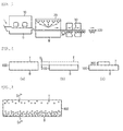
- FIG. 1 is a schematic diagram showing a conventional method for manufacturing a float glass by a typical float process.
- a conventional method for manufacturing a float glass is performed with a melting furnace 10, a float bath 20, and an annealing furnace 30.
- a raw glass material is fed into the melting furnace 10 to form a molten glass G.
- the formed molten glass G is injected into the float bath 20.
- molten metal M such as molten tin (Sn) or molten tin alloy at 600 to 1,050°C is contained in the float bath 20.
- a reducing atmosphere including hydrogen and/or nitrogen gas is created over the molten metal M to prevent oxidation of the molten metal M.
- the molten glass G When the molten glass G is continuously fed onto the molten metal M contained in the float bath 20, the molten glass G having a viscosity and weight lower than those of the molten metal M floats and spreads on the molten metal M and flows to the downstream of the float bath 20. In this process, the molten glass G reaches an equilibrium thickness according to its own surface tension and gravity, and a glass strip or ribbon solidified to a certain degree is formed. The molten glass ribbon is pulled toward the annealing furnace by a roller adjacent to an outlet of the float bath 20. The glass cooled in the annealing furnace is cut into an appropriate size and completes as a float glass product 100.
- a float bath 20 containing molten metal M, particularly molten tin, is used and so tin components are present in the float glass 100. That is, the bottom face of the float glass 100 directly contacts the molten tin in the float bath 20, and thus the tin component may penetrate the float glass 100 through the bottom face. Also, by the atmosphere in the float bath 20, the tin component of the molten tin may also penetrate the glass 100 through the top face of the float glass 100. The tin component penetrating the float glass 100 may diffuse, and thus 1 to 1,000 ppm or more of the tin component may be contained in the float glass 100.
- tin (Sn 0 ) is oxidized by oxygen that is present in a very small amount and penetrates the glass in the form of Sn 2+ through an ion exchange reaction with Na+ in the glass.
- the penetration rate of Sn 2+ is much higher than that of Sn 0 or Sn 4+ .
- Sn 2+ that starts to penetrate like the above may convert into Sn 4+ through an oxidation-reduction reaction with Fe 3+ present in the glass ( Journal of Non-Crystalline Solids, 2001, 282, 188 ).
- the tin component on the surface of the float glass 100 is substantially present in the form of Sn 2+ and a very small amount of tin component is present in the form of Sn 0 or Sn 4+ .
- the diffusion depth of Sn 2+ may be up to about 20 um on the basis of the glass surface contacting the molten tin. ( J. Noncryst. Solids, 2000, 265, 133-142 ).
- reaction Formula (1) Sn 2+ + 2Ag + ⁇ Sn 4+ + 2Ag 0 ; nAg 0 ⁇ (Ag 0 ) n
- the yellowing phenomenon not only occurs in the silver powder but may also occur in a conductive paste containing another metal powder.
- a representative example of another metal powder used as the conductive paste may include copper powder.
- copper may react with the tin component of a molten tin according to the following Reaction Formula (2) and may have a ruby color.
- Formula (2) Sn 2+ + 2Cu + ⁇ Sn 4+ + 2Cu 0 ; nCu 0 ⁇ (Cu 0 ) n
- the ruby color shows an absorption spectrum at about 450 nm by free copper ions and at about 570 nm by (Cu0) n nanocrystal on a spectrum ( ref. J. Noncryst. Solids, 2006, 352, 3910-3913 ).
- the yellowing phenomenon may occur due to the tin component contained in the float glass 100 during the manufacturing of the conductive substrate, and the yellowing phenomenon may cause a reduction in transmittance of the float glass 100. As a result, the quality of the float glass 100 and the conductive substrate using the float glass 100 may deteriorate.
- the present disclosure is designed to solve the problems of the prior art, and therefore it is an object of the present disclosure to provide a conductive substrate and a method for manufacturing the same, in which a yellowing phenomenon does not occur in a float glass even when a conductive pattern is first formed on the float glass manufactured by a float process and then undergoes a firing process.
- a method for manufacturing a conductive substrate according to the present disclosure includes: manufacturing a float glass by injecting molten glass onto a molten tin contained in a float bath; removing a top face of the float glass not contacting the molten tin, by a predetermined thickness; and forming a conductive pattern on the top face of the float glass, which was removed by a predetermined thickness.
- the top face of the float glass is removed by a thickness of 5 um or less.
- the removing of the top face of the float glass is performed by grinding, lapping, polishing, compounding polishing, plasma etching, or ion beam etching.
- the removing of the top face of the float glass is performed by wet etching or dry etching.
- the wet etching is performed using an etching solution comprising at least one selected from the group consisting of hydrofluoric acid, hydrochloric acid, sulfuric acid, and nitric acid.
- the conductive pattern is formed by printing a conductive paste by offset printing, inkjet printing, screen printing, or gravure printing.
- the conductive paste comprises at least one selected from the group consisting of copper, silver, gold, iron, nickel, and aluminum.
- the method further includes firing the float glass after the forming of the conductive pattern.
- a method for manufacturing a float glass according to the present disclosure includes: forming a glass ribbon by injecting molten glass onto a molten tin contained in a float bath; cooling the glass ribbon outside the float bath; and removing a top face of the cooled glass ribbon not contacting the molten tin during the forming of the glass ribbon, by a predetermined thickness.
- the top face of the cooled glass ribbon is removed by a thickness of 5 um or less.
- a conductive substrate includes: a float glass manufactured by injecting molten glass onto a molten tin contained in a float bath and having a top face not contacting the molten tin removed by a predetermined thickness; and a conductive pattern formed on the top face of the float glass.
- the top face of the float glass is removed by a thickness of 5 um or less.
- a display device includes the above conductive substrate.
- a float glass according to the present disclosure is manufactured by injecting molten glass onto a molten tin contained in a float bath and having a top face not contacting the molten tin removed by a predetermined thickness.
- the predetermined thickness is 5 um or less.
- the tin component is removed from the float glass manufactured by a float process by cutting a region where the tin component is diffused.
- the float glass is divided into a bottom face, which directly contacts the molten tin in the float bath, and a top face, which does not directly contact the molten tin, such that the top face of the float glass is removed by a predetermined thickness.
- the amount of tin component diffused in the top face of the float glass is smaller than that in the bottom face which directly contacts the molten tin.
- the top face of the float glass is removed by a predetermined thickness from the entire top face of the float glass, in which the tin component is diffused, and a conductive pattern is formed on the resulting top face of the float glass, it is possible to efficiently prevent the yellowing phenomenon from occurring even when the float glass undergoes a firing process at a high temperature as well as at a low temperature.
- a conductive substrate according to the present disclosure includes a float glass manufactured by a float process and having a top face removed by a predetermined thickness and a conductive pattern disposed on the top face of the float glass.
- FIG. 2 is a schematic diagram showing the structure of a conductive substrate in accordance with a preferred embodiment of the present disclosure.
- the float glass 100 is manufactured by a float process as shown in FIG. 1 .
- the float glass 100 manufactured by the float process is a flat glass whose cross-section may be shown as in (a) of FIG. 2 .
- the float glass 100 may have a thickness of 0.5 to 5 mm, but the present disclosure is not particularly limited to the thickness.
- the composition of the floating glass 100 may vary.
- the top face T of the float glass 100 is a surface that does not directly contact the molten tin contained in a float bath when the float glass 100 is manufactured by the float process. That is, the float glass 100 is manufactured by floating the molten glass on the molten tin contained in the float bath.
- a bottom face B of the float glass 100 directly contacts the molten tin, whereas, the top face T does not directly contact the molten tin.
- the top face T of the float glass 100 which does not directly contact the molten tin, is removed by a predetermined thickness D.
- the reason that the top face T of the float glass 100 is removed by a predetermined thickness D, and not the bottom face D, is because there is a difference in the amount of tin component between the bottom face B and the top face T of the floating glass 100.
- FIG. 3 is a schematic diagram showing a state in which the tin component is included in the float glass 100 manufactured by the float process.
- the tin component in the form of Sn 0 and Sn 4+ may be included in the glass manufactured by the float process, but since the tin component mainly included is Sn 2+ , only Sn 2+ is shown in FIG. 3 .
- the bottom face B of the float glass 100 since the bottom face B of the float glass 100 directly contacts the molten tin in the float bath, the bottom face B includes a greater amount of tin component.
- the top face T of the float glass 100 does not directly contact the molten tin, and the tin component can penetrate the top face T only by the atmosphere of the float bath. As a result, the top face T contains a smaller amount of tin component.
- the bottom face B of the float glass 100 in which a greater amount of tin component is diffused, is not removed, but the top face T, in which a small amount of tin component is diffused, is removed as shown by the dotted line in FIG. 2 . Accordingly, when a conductive pattern 200 is formed thereon, it is possible to achieve the effect of substantially removing the tin component that may cause a yellowing phenomenon, even if a much smaller thickness is cut.
- the top face T of the float glass 100 is removed by a thickness of 5 um or less.
- the tin component can be diffused up to a depth of 20 um or more in the bottom face B of the float glass 100, whereas, the tin component is diffused only up to a depth of 5 um or less in the top face T of the float glass 100.
- the top face T of the float glass 100 of the conductive substrate according to the present disclosure is removed in the above-described manner, and thus it is possible to prevent the yellowing phenomenon even when the top face T is removed by a thickness of 5 um or less.
- the float glass 100 may be removed by just cutting a small thickness, and thus it is possible to significantly reduce the cost and time required to remove the tin component so as to prevent the yellowing phenomenon.
- the conductive pattern 200 is formed on the top face T of the float glass 100 which is removed by a predetermined thickness.
- the conductive pattern 200 may be formed of a conductive paste including at least one selected from the group consisting of copper, silver, gold, iron, nickel, and aluminum as a conductive material.
- the conductive substrate according to the present disclosure may be used as a heating element or an electromagnetic wave shielding filter. Accordingly, the conductive pattern 200 may be a conductive heating pattern or an electromagnetic wave shielding conductive pattern 200. However, the present disclosure is not particularly limited to the type of the conductive pattern 200.
- the heating element may be used as a glass for buildings or vehicles.
- the heating element may be used as a window for buildings or vehicles in which the conductive pattern generates heat when power is applied thereto.
- a separate glass substrate may be further included.
- the electromagnetic wave shielding filter may further include a ground.
- the ground may be provided on the top face T of the float glass 100, which is cut by a predetermined thickness to remove the tin component, and may be disposed to surround the circumference of the conductive pattern.
- the electromagnetic wave shielding filter may be included in an optical filter.
- the optical filter may further include a functional film.
- the optical filter may include an anti-reflective film, a near-infrared ray shielding film, and a color compensation film.
- the optical filter may include at least one selected from the group consisting of the electromagnetic wave shielding filter, the anti-reflective film, the near-infrared ray shielding film, and the color compensation film.
- the optical filter may further include other types of functional films according to the design specifications in addition to the above-mentioned functional films.
- a display device may include the above-described conductive substrate.
- the display device according to the present disclosure may include a conductive shielding filter as the conductive substrate.
- an electromagnetic wave shielding filter may be independently attached to the display device, or an optical filter including an electromagnetic wave shielding filter may be attached to the display device.
- the conductive substrate according to the present disclosure may be included in various types of display devices such as plasma display panels (PDPs), liquid crystal displays (LCDs), cathode-ray tube (CRTs), etc.
- PDPs plasma display panels
- LCDs liquid crystal displays
- CRTs cathode-ray tube
- the plasma display panel may include two panels.
- the electromagnetic wave shielding filter according to the present disclosure may be attached to one side of the panel.
- the plasma display panel may further include at least one functional film in addition to the electromagnetic wave shielding filter.
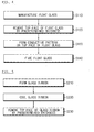
- FIG. 4 is a schematic flowchart showing a method for manufacturing a conductive substrate in accordance with a preferred embodiment of the present disclosure.
- a float glass 100 is manufactured by a typical float method (S110). That is, as shown in FIG. 1 , the float glass 100 is manufactured by injecting the molten glass on a molten tin contained in a float bath to float thereon. The tin component is contained in a top face T and a bottom face B of the float glass 100.
- the top face T of the float glass 100 which does not directly contact the molten tin in the float bath, is removed by a predetermined thickness D (S120).
- a predetermined thickness D S120.
- the top face T of the float glass 100 is removed by a thickness of 5 um or less.
- the top face T of the float glass 100 in which a smaller amount of tin component is diffused, is cut and removed, and thus it is possible to efficiently remove the tin component that causes the yellowing phenomenon, even though the top face T is removed by a thickness of 5 um or less.
- the bottom face B of the float glass 100 if the bottom face B of the float glass 100 is cut, the bottom face B of the float glass 100 has to be removed by a greater thickness, e.g., a thickness of 30 um or more to substantially remove the tin component that causes the yellowing phenomenon. In this case, not only does it require much more cost and time to cut the float glass 100, the thickness of the float glass 100 is further reduced.
- step S120 may be performed by grinding using a grinder, lapping, polishing, compounding polishing, plasma etching, or ion beam etching.
- the top face T of the float glass 100 in which the tin component is diffused may be removed by a chemical method or a physical method.
- the top face T may be removed by a wet etching process or a dry etching process.
- the wet etching process may be performed using an etching solution containing at least one selected from the group consisting of hydrofluoric acid, hydrochloric acid, sulfuric acid, and nitric acid.
- the etching solution may be prepared by mixing 50% acidic solution containing 95% HCL and 5% HF with 50% deionized water.
- the etching solution may contain 1 to 90 wt% HF such as in HF: H 2 O and in HF:HCl:H 2 O.
- a conductive pattern 200 is formed on the top face T of the float glass 100 (S130).
- the conductive pattern 200 may be formed by printing a conductive paste by offset printing, inkjet printing, screen printing, or gravure printing.
- the conductive paste may include at least one metal powder selected from the group consisting of copper, silver, gold, iron, nickel, and aluminum as a conductive material.
- the conductive paste may further include an organic binder and/or a glass frit in addition to the above-mentioned conductive materials.
- the organic binder may be volatilized during a firing process.
- the organic binder may include polyacrylic resin, polyurethane resin, polyester resin, polyolefin resin, polycarbonate resin, cellulose resin, polyimide resin, polyethylene naphthalate resin, and modified epoxy, but the present disclosure is not limited thereto.
- the conductive paste further includes the glass frit
- the glass frit may be any one of glass frits well known in the art, and the present disclosure is not particularly limited to the type of the glass frit.
- the conductive paste may further include a solvent.
- the solvent may include butyl carbitol acetate, carbitol acetate, cyclohexanone, cellosolve acetate, and terpineol, but the present disclosure is not particularly limited to the type of the solvent.
- the conductive paste may be prepared by dispersing a conductive material, an organic binder, and a glass frit in a solvent. More specifically, an organic binder resin solution is prepared by dissolving an organic binder in a solvent, a glass frit is added to the resulting mixture, a metal powder such as copper, silver, gold, iron, nickel, or aluminum powder as conductive material is added and mixed to the resulting mixture, and then the resulting mixture of the metal powder and the glass frit is uniformly dispersed by a three-roll mill, thereby preparing the conductive paste.
- an organic binder resin solution is prepared by dissolving an organic binder in a solvent
- a glass frit is added to the resulting mixture
- a metal powder such as copper, silver, gold, iron, nickel, or aluminum powder as conductive material is added and mixed to the resulting mixture, and then the resulting mixture of the metal powder and the glass frit is uniformly dispersed by a three-roll mill, thereby preparing the conductive paste.
- the conductive paste when the conductive paste including the conductive material, the organic binder, the glass frit, and the solvent is used, the conductive paste may contain 50 to 90 wt% conductive material, 1 to 20 wt% organic binder, 0.1 to 10 wt% glass frit, and 1 to 20 wt% solvent.
- the method for manufacturing the conductive substrate may further include firing the conductive pattern 200 formed on the top face T of the float glass 100 (S140).
- the firing temperature may be 400 to 700°C.
- the glass frit when the glass frit is contained in the conductive paste and the firing is performed at a temperature of 400 to 700°C, the glass frit is softened to increase the adhesion between the conductive pattern 200 and the float glass 100.
- the metal powder such as the silver component, for example, contained in the conductive paste may melt and fuse to the glass 100, which is problematic.
- the glass frit when the glass frit is contained in the conductive paste, the glass frit may not completely melt, and the organic matter may not be removed, thereby reducing the adhesion between the silver and the glass.
- a deformation of the float glass 100 such as a strain point due to bending or unevenness of the surface of the float glass 100 may occur, and thus the deformed float glass 100 may not be suitable for display devices.
- the method for manufacturing the conductive substrate according to the present disclosure may further include blackening the conductive pattern 200 formed on the top face T of the float glass 100.
- a blackening material may be added to the conductive paste for forming the pattern, or the conductive paste may be blackened after printing and firing.
- the blackening material added to the conductive paste may include metal oxide, carbon black, carbon nanotubes, black pigment, colored glass frit, etc.
- the conductive paste may preferably include 50 to 90 wt% conductive heating material, 1 to 20 wt% organic binder, 1 to 10 wt% blackening material, 0.1 to 10 wt% glass frit, and 1 to 20 wt% solvent.
- the conductive paste may preferably include 50 to 90 wt% conductive material, 1 to 20 wt% organic binder, 0.1 to 10 wt% glass frit, and 1 to 20 wt% solvent.
- the blackening treatment after the firing process may be performed by immersing the conductive pattern in an oxidizing solution, for example, a solution containing Fe or Cu ions, immersing the conductive pattern in a solution containing halogen ions such as chloride ions, immersing the conductive pattern in hydrogen peroxide or nitric acid, or processing the conductive pattern using a halogen gas.
- the top face T of the float glass 100 may be removed during the process of manufacturing the conductive substrate.
- the top face T of the float glass 100 may be removed during the process of manufacturing the float glass 100. That is, according to the present disclosure, a finished product of the float glass 100 may be cut and used to manufacture the conductive substrate, or a finished product of the float glass 100 from which the top face T is removed may be used to manufacture the conductive substrate.
- the float glass 100 according to the present disclosure is manufactured by the float process, in which the molten glass is injected onto the molten tin contained in the float bath, and the top face T of the float glass 100, which does not directly contact the molten tin, is removed by a predetermined thickness D.
- the top face T of the float glass 100 may be removed by a thickness of 5 um or less.
- FIG. 5 is a schematic flowchart showing a method for manufacturing a float glass in accordance with a preferred embodiment of the present disclosure.
- a glass ribbon is formed by injecting molten glass onto a molten tin contained in a float bath (S210).
- the glass ribbon formed in the float bath is cooled outside the float bath (S220), and then the top face T of the cooled glass ribbon, which does not directly contact the molten tin, is removed by a predetermined thickness (S230).
- the top face T of the glass ribbon may be removed by a thickness of 5 um or less.
- step S230 may be performed by grinding, lapping, polishing, compounding polishing, plasma etching, or ion beam etching.
- step S230 may be performed by wet etching or dry etching.
- each float glass was etched using an etching solution containing HF and H 2 O in a weight ratio of 1:10 so as to cut the top face of the float glass by a thickness of about 4.2 um.
- a conductive pattern was formed on each float glass, whose top face was removed, using a mask of a mesh pattern and Ag paste, and then the four pieces of float glass were fired at 620°C, 650°C, 680°C and 700°C, respectively. Thereafter, the transmittance of light at a wavelength of 420 nm was measured from the four pieces of float glass, and the results are shown in FIG. 6 .
- the transmittance of light at a wavelength of 420 nm measured from all the conductive substrates fired at 620°C, 650°C, 680°C and 700°C was 60% or higher.
- the transmittance of light did not significantly change at a firing-temperature of 620°C, but was significantly reduced when the firing temperature was increased, compared to that of the Example of the present disclosure.
- the reason that the transmittance of the conductive substrates of the Comparative Example was significantly reduced when the firing temperature was increased was because the yellowing phenomenon was increased in the float glass included in the conductive substrates of the Comparative Example as the firing temperature was progressively increased from 620°C to 650°C, 680°C and 700°C. On the contrary, in the case of the conductive substrates according to the Example of the present disclosure, the yellowing phenomenon hardly occurred in the float glass, and thus there was no significant difference in transmittance even when the firing temperature was increased.
Landscapes
- Chemical & Material Sciences (AREA)
- Materials Engineering (AREA)
- Engineering & Computer Science (AREA)
- Chemical Kinetics & Catalysis (AREA)
- General Chemical & Material Sciences (AREA)
- Geochemistry & Mineralogy (AREA)
- Life Sciences & Earth Sciences (AREA)
- Organic Chemistry (AREA)
- Surface Treatment Of Glass (AREA)
- Glass Compositions (AREA)
- Gas-Filled Discharge Tubes (AREA)
- Manufacturing Of Electric Cables (AREA)
- Devices For Indicating Variable Information By Combining Individual Elements (AREA)
Applications Claiming Priority (3)
| Application Number | Priority Date | Filing Date | Title |
|---|---|---|---|
| KR20090072682 | 2009-08-07 | ||
| KR1020100064954A KR101245278B1 (ko) | 2009-08-07 | 2010-07-06 | 전도성 기판 및 이의 제조 방법 |
| PCT/KR2010/004738 WO2011016631A2 (fr) | 2009-08-07 | 2010-07-20 | Plaque de base conductrice de lélectricité et procédé de fabrication associé |
Publications (2)
| Publication Number | Publication Date |
|---|---|
| EP2463244A2 true EP2463244A2 (fr) | 2012-06-13 |
| EP2463244A4 EP2463244A4 (fr) | 2013-03-06 |
Family
ID=43774199
Family Applications (1)
| Application Number | Title | Priority Date | Filing Date |
|---|---|---|---|
| EP10806606A Withdrawn EP2463244A4 (fr) | 2009-08-07 | 2010-07-20 | Plaque de base conductrice de l électricité et procédé de fabrication associé |
Country Status (6)
| Country | Link |
|---|---|
| US (1) | US20120327613A1 (fr) |
| EP (1) | EP2463244A4 (fr) |
| JP (1) | JP2013501694A (fr) |
| KR (1) | KR101245278B1 (fr) |
| CN (1) | CN102686523A (fr) |
| WO (1) | WO2011016631A2 (fr) |
Families Citing this family (5)
| Publication number | Priority date | Publication date | Assignee | Title |
|---|---|---|---|---|
| JP5835654B2 (ja) * | 2011-08-31 | 2015-12-24 | 日本電気硝子株式会社 | 強化ガラス基板の製造方法 |
| WO2014175362A1 (fr) * | 2013-04-24 | 2014-10-30 | 旭硝子株式会社 | Procédé de production de verre à vitre flotté |
| KR101489241B1 (ko) * | 2013-10-01 | 2015-02-04 | 주식회사 이코니 | 전처리 공정을 포함한 유리기판 슬림에칭 방법 |
| JP6115466B2 (ja) * | 2013-12-26 | 2017-04-19 | 旭硝子株式会社 | フロート板ガラスの製造方法 |
| WO2020105236A1 (fr) * | 2018-11-20 | 2020-05-28 | 三井金属鉱業株式会社 | Corps multicouche |
Family Cites Families (17)
| Publication number | Priority date | Publication date | Assignee | Title |
|---|---|---|---|---|
| JPH10255669A (ja) * | 1997-03-14 | 1998-09-25 | Nippon Electric Glass Co Ltd | フラットパネルディスプレイ用ガラス基板及びそれを用いたプラズマディスプレイ装置 |
| JP2001035393A (ja) * | 1999-07-27 | 2001-02-09 | Central Glass Co Ltd | 透明絶縁性被膜形成用低融点ガラス |
| JP2001089191A (ja) * | 1999-09-27 | 2001-04-03 | Nippon Sheet Glass Co Ltd | ディスプレイ用ガラス基板の製造方法及び該製造方法により製造されたディスプレイ用ガラス基板 |
| JP3389240B2 (ja) * | 1999-12-21 | 2003-03-24 | 松下電器産業株式会社 | プラズマディスプレイパネルおよびその製造方法 |
| CN1159732C (zh) * | 2000-10-30 | 2004-07-28 | 广东肇庆风华电子工程开发有限公司 | 片式电感器用可镀端浆 |
| JP4374993B2 (ja) * | 2002-11-29 | 2009-12-02 | パナソニック株式会社 | 画像表示装置 |
| KR100643043B1 (ko) * | 2002-11-29 | 2006-11-10 | 마쯔시다덴기산교 가부시키가이샤 | 화상 표시 장치 및 그것에 이용하는 유리 기판의 평가 방법 |
| CN100337952C (zh) * | 2002-11-29 | 2007-09-19 | 松下电器产业株式会社 | 用于图像显示装置的玻璃基板的制造方法 |
| US7495393B2 (en) * | 2002-11-29 | 2009-02-24 | Panasonic Corporation | Image display device and method for manufacturing same |
| JP2004348046A (ja) * | 2003-05-26 | 2004-12-09 | Nippon Sheet Glass Co Ltd | ガラス基板 |
| JP2006244747A (ja) * | 2005-03-01 | 2006-09-14 | Central Glass Co Ltd | ディスプレーパネル用基板及びその製造方法 |
| JP4934993B2 (ja) * | 2005-05-25 | 2012-05-23 | 住友電気工業株式会社 | 導電性ペーストおよびそれを用いた配線基板 |
| NO324539B1 (no) * | 2005-06-14 | 2007-11-19 | Thin Film Electronics Asa | Fremgangsmate i fabrikasjonen av en ferroelektrisk minneinnretning |
| CN100519456C (zh) * | 2006-01-10 | 2009-07-29 | 桂林迪华特种玻璃有限公司 | 一种微晶玻璃的制备方法 |
| KR100863408B1 (ko) * | 2007-04-03 | 2008-10-14 | 주식회사 엘지화학 | 흑화처리된 전자파 차폐 유리 및 그 제조방법 |
| WO2008140234A1 (fr) * | 2007-05-10 | 2008-11-20 | Lg Chem, Ltd. | Verre noirci blindé contre les interférences électromagnétiques, et sa méthode de production |
| JP2009155179A (ja) * | 2007-12-27 | 2009-07-16 | Nippon Electric Glass Co Ltd | フラットパネルディスプレイ用ガラス基板 |
-
2010
- 2010-07-06 KR KR1020100064954A patent/KR101245278B1/ko active Active
- 2010-07-20 US US13/389,381 patent/US20120327613A1/en not_active Abandoned
- 2010-07-20 CN CN2010800444182A patent/CN102686523A/zh active Pending
- 2010-07-20 JP JP2012523558A patent/JP2013501694A/ja active Pending
- 2010-07-20 EP EP10806606A patent/EP2463244A4/fr not_active Withdrawn
- 2010-07-20 WO PCT/KR2010/004738 patent/WO2011016631A2/fr not_active Ceased
Also Published As
| Publication number | Publication date |
|---|---|
| EP2463244A4 (fr) | 2013-03-06 |
| KR101245278B1 (ko) | 2013-03-19 |
| KR20110015368A (ko) | 2011-02-15 |
| WO2011016631A3 (fr) | 2011-05-05 |
| JP2013501694A (ja) | 2013-01-17 |
| WO2011016631A2 (fr) | 2011-02-10 |
| CN102686523A (zh) | 2012-09-19 |
| US20120327613A1 (en) | 2012-12-27 |
Similar Documents
| Publication | Publication Date | Title |
|---|---|---|
| US7838451B2 (en) | Alkali-free glass and liquid crystal display panel | |
| US8715387B2 (en) | Process for making silver powder particles with small size crystallites | |
| JP4802248B2 (ja) | 導電性パターンの製造方法およびこれによって製造された導電性パターン | |
| US20120327613A1 (en) | Conductive substrate and method for manufacturing the same | |
| US20150266098A1 (en) | Process for making silver powder particles with very small size crystallites | |
| EP1020890B1 (fr) | Structure transparente et électro-conductive, procédé pour sa production, fluide formant une couche transparente et électro-conductive pour la production de la structure, et procédé pour la production du fluide | |
| JP2013503443A (ja) | 銀厚膜ペースト組成物および太陽電池用導電体におけるその使用 | |
| JPWO2001046979A1 (ja) | プラズマディスプレイパネルおよびその製造方法 | |
| EP2145336B1 (fr) | Verre noirci blindé contre les interférences électromagnétiques, et sa méthode de production | |
| KR101091853B1 (ko) | 전도성 패턴의 제조방법 및 이에 의해 제조된 전도성 패턴 | |
| US6376400B1 (en) | Low melting point glass for covering electrodes, and glass ceramic composition for covering electrodes | |
| EP1460046A1 (fr) | Substrat de verre avec pellicule de couleur, solution contenant des particules destinee a la fabrication d'une pellicule de couleur et procede de fabrication d'un substrat de verre avec une pellicule de couleur | |
| KR100864152B1 (ko) | 전도성 패턴이 흑화처리된 전자파 차폐 유리 및 그제조방법 | |
| JP2007204295A (ja) | ディスプレイ基板用ガラス板及びその製造方法 | |
| WO2004106251A1 (fr) | Feuille de verre pour substrat d'affichage | |
| JP4016560B2 (ja) | 電極被覆用低融点ガラスおよび電極被覆用ガラスセラミック組成物 | |
| KR101188753B1 (ko) | 전도성 패턴의 제조방법 및 이에 의해 제조된 전도성 패턴 | |
| JP2008059928A (ja) | 透明導電膜の製造方法及び透明導電膜 | |
| WO2003045858A1 (fr) | Procede de fabrication de verre plat a partir de dechets de verre |
Legal Events
| Date | Code | Title | Description |
|---|---|---|---|
| PUAI | Public reference made under article 153(3) epc to a published international application that has entered the european phase |
Free format text: ORIGINAL CODE: 0009012 |
|
| 17P | Request for examination filed |
Effective date: 20120228 |
|
| AK | Designated contracting states |
Kind code of ref document: A2 Designated state(s): AL AT BE BG CH CY CZ DE DK EE ES FI FR GB GR HR HU IE IS IT LI LT LU LV MC MK MT NL NO PL PT RO SE SI SK SM TR |
|
| RIN1 | Information on inventor provided before grant (corrected) |
Inventor name: PARK, JONG-WUK Inventor name: KIM, SO-WON Inventor name: CHOI, HYEON Inventor name: CHUN, SANG-KI Inventor name: KIM, SANG-HO |
|
| RIN1 | Information on inventor provided before grant (corrected) |
Inventor name: KIM, SO-WON Inventor name: CHOI, HYEON Inventor name: CHUN, SANG-KI Inventor name: PARK, JONG-WUK Inventor name: KIM, SANG-HO |
|
| DAX | Request for extension of the european patent (deleted) | ||
| A4 | Supplementary search report drawn up and despatched |
Effective date: 20130204 |
|
| RIC1 | Information provided on ipc code assigned before grant |
Ipc: C03B 18/02 20060101ALI20130129BHEP Ipc: C03C 19/00 20060101ALI20130129BHEP Ipc: C03C 17/06 20060101ALI20130129BHEP Ipc: C03C 15/00 20060101AFI20130129BHEP |
|
| STAA | Information on the status of an ep patent application or granted ep patent |
Free format text: STATUS: THE APPLICATION IS DEEMED TO BE WITHDRAWN |
|
| 18D | Application deemed to be withdrawn |
Effective date: 20160301 |