EP2463695B1 - Procédé pour réaliser un guide optique à fente sur silicium - Google Patents
Procédé pour réaliser un guide optique à fente sur silicium Download PDFInfo
- Publication number
- EP2463695B1 EP2463695B1 EP11192997.2A EP11192997A EP2463695B1 EP 2463695 B1 EP2463695 B1 EP 2463695B1 EP 11192997 A EP11192997 A EP 11192997A EP 2463695 B1 EP2463695 B1 EP 2463695B1
- Authority
- EP
- European Patent Office
- Prior art keywords
- silicon
- insulating
- wall
- semi
- layer
- Prior art date
- Legal status (The legal status is an assumption and is not a legal conclusion. Google has not performed a legal analysis and makes no representation as to the accuracy of the status listed.)
- Not-in-force
Links
- 229910052710 silicon Inorganic materials 0.000 title claims description 81
- 239000010703 silicon Substances 0.000 title claims description 81
- 230000003287 optical effect Effects 0.000 title claims description 21
- 238000000034 method Methods 0.000 title claims description 18
- XUIMIQQOPSSXEZ-UHFFFAOYSA-N Silicon Chemical compound [Si] XUIMIQQOPSSXEZ-UHFFFAOYSA-N 0.000 claims description 81
- 239000000758 substrate Substances 0.000 claims description 19
- 229910021421 monocrystalline silicon Inorganic materials 0.000 claims description 18
- 239000012535 impurity Substances 0.000 claims description 13
- 230000008569 process Effects 0.000 claims description 11
- 230000008021 deposition Effects 0.000 claims description 7
- 238000004519 manufacturing process Methods 0.000 claims description 6
- 230000003647 oxidation Effects 0.000 claims description 6
- 238000007254 oxidation reaction Methods 0.000 claims description 6
- 238000005498 polishing Methods 0.000 claims description 3
- 239000000126 substance Substances 0.000 claims description 3
- 239000010408 film Substances 0.000 claims 4
- 238000009412 basement excavation Methods 0.000 claims 1
- 230000001590 oxidative effect Effects 0.000 claims 1
- 239000010409 thin film Substances 0.000 claims 1
- 239000010410 layer Substances 0.000 description 67
- VYPSYNLAJGMNEJ-UHFFFAOYSA-N Silicium dioxide Chemical compound O=[Si]=O VYPSYNLAJGMNEJ-UHFFFAOYSA-N 0.000 description 8
- 239000000969 carrier Substances 0.000 description 8
- 230000000873 masking effect Effects 0.000 description 8
- 229910052814 silicon oxide Inorganic materials 0.000 description 8
- 239000000463 material Substances 0.000 description 7
- LIVNPJMFVYWSIS-UHFFFAOYSA-N silicon monoxide Chemical compound [Si-]#[O+] LIVNPJMFVYWSIS-UHFFFAOYSA-N 0.000 description 7
- 229910004298 SiO 2 Inorganic materials 0.000 description 6
- 238000005530 etching Methods 0.000 description 6
- 239000011810 insulating material Substances 0.000 description 5
- 238000000137 annealing Methods 0.000 description 4
- 229910052751 metal Inorganic materials 0.000 description 4
- 239000002184 metal Substances 0.000 description 4
- 229910052581 Si3N4 Inorganic materials 0.000 description 3
- 238000002513 implantation Methods 0.000 description 3
- 239000012212 insulator Substances 0.000 description 3
- 239000011347 resin Substances 0.000 description 3
- 229920005989 resin Polymers 0.000 description 3
- HQVNEWCFYHHQES-UHFFFAOYSA-N silicon nitride Chemical compound N12[Si]34N5[Si]62N3[Si]51N64 HQVNEWCFYHHQES-UHFFFAOYSA-N 0.000 description 3
- 230000008901 benefit Effects 0.000 description 2
- 230000015572 biosynthetic process Effects 0.000 description 2
- 150000001875 compounds Chemical class 0.000 description 2
- 238000009413 insulation Methods 0.000 description 2
- 230000005693 optoelectronics Effects 0.000 description 2
- 238000000206 photolithography Methods 0.000 description 2
- 150000003376 silicon Chemical class 0.000 description 2
- JBRZTFJDHDCESZ-UHFFFAOYSA-N AsGa Chemical compound [As]#[Ga] JBRZTFJDHDCESZ-UHFFFAOYSA-N 0.000 description 1
- 229910017214 AsGa Inorganic materials 0.000 description 1
- 230000035508 accumulation Effects 0.000 description 1
- 238000009825 accumulation Methods 0.000 description 1
- 230000009471 action Effects 0.000 description 1
- 229910052782 aluminium Inorganic materials 0.000 description 1
- XAGFODPZIPBFFR-UHFFFAOYSA-N aluminium Chemical compound [Al] XAGFODPZIPBFFR-UHFFFAOYSA-N 0.000 description 1
- 229910021417 amorphous silicon Inorganic materials 0.000 description 1
- 230000004888 barrier function Effects 0.000 description 1
- 239000003990 capacitor Substances 0.000 description 1
- 238000003486 chemical etching Methods 0.000 description 1
- 238000006243 chemical reaction Methods 0.000 description 1
- 239000013078 crystal Substances 0.000 description 1
- 238000010586 diagram Methods 0.000 description 1
- 238000009792 diffusion process Methods 0.000 description 1
- 238000001312 dry etching Methods 0.000 description 1
- 238000010292 electrical insulation Methods 0.000 description 1
- 238000005516 engineering process Methods 0.000 description 1
- 230000003631 expected effect Effects 0.000 description 1
- 239000007943 implant Substances 0.000 description 1
- 238000011065 in-situ storage Methods 0.000 description 1
- 230000001939 inductive effect Effects 0.000 description 1
- 230000002452 interceptive effect Effects 0.000 description 1
- 238000005468 ion implantation Methods 0.000 description 1
- 230000010363 phase shift Effects 0.000 description 1
- 229910021420 polycrystalline silicon Inorganic materials 0.000 description 1
- 230000009467 reduction Effects 0.000 description 1
- 230000000284 resting effect Effects 0.000 description 1
- HBMJWWWQQXIZIP-UHFFFAOYSA-N silicon carbide Chemical compound [Si+]#[C-] HBMJWWWQQXIZIP-UHFFFAOYSA-N 0.000 description 1
- 229910010271 silicon carbide Inorganic materials 0.000 description 1
- XUIMIQQOPSSXEZ-NJFSPNSNSA-N silicon-30 atom Chemical compound [30Si] XUIMIQQOPSSXEZ-NJFSPNSNSA-N 0.000 description 1
- 239000002356 single layer Substances 0.000 description 1
Images



Classifications
-
- G—PHYSICS
- G02—OPTICS
- G02B—OPTICAL ELEMENTS, SYSTEMS OR APPARATUS
- G02B6/00—Light guides; Structural details of arrangements comprising light guides and other optical elements, e.g. couplings
- G02B6/10—Light guides; Structural details of arrangements comprising light guides and other optical elements, e.g. couplings of the optical waveguide type
- G02B6/12—Light guides; Structural details of arrangements comprising light guides and other optical elements, e.g. couplings of the optical waveguide type of the integrated circuit kind
- G02B6/122—Basic optical elements, e.g. light-guiding paths
- G02B6/1223—Basic optical elements, e.g. light-guiding paths high refractive index type, i.e. high-contrast waveguides
-
- B—PERFORMING OPERATIONS; TRANSPORTING
- B82—NANOTECHNOLOGY
- B82Y—SPECIFIC USES OR APPLICATIONS OF NANOSTRUCTURES; MEASUREMENT OR ANALYSIS OF NANOSTRUCTURES; MANUFACTURE OR TREATMENT OF NANOSTRUCTURES
- B82Y20/00—Nanooptics, e.g. quantum optics or photonic crystals
-
- G—PHYSICS
- G02—OPTICS
- G02B—OPTICAL ELEMENTS, SYSTEMS OR APPARATUS
- G02B6/00—Light guides; Structural details of arrangements comprising light guides and other optical elements, e.g. couplings
- G02B6/10—Light guides; Structural details of arrangements comprising light guides and other optical elements, e.g. couplings of the optical waveguide type
- G02B6/107—Subwavelength-diameter waveguides, e.g. nanowires
-
- G—PHYSICS
- G02—OPTICS
- G02B—OPTICAL ELEMENTS, SYSTEMS OR APPARATUS
- G02B6/00—Light guides; Structural details of arrangements comprising light guides and other optical elements, e.g. couplings
- G02B6/10—Light guides; Structural details of arrangements comprising light guides and other optical elements, e.g. couplings of the optical waveguide type
- G02B6/12—Light guides; Structural details of arrangements comprising light guides and other optical elements, e.g. couplings of the optical waveguide type of the integrated circuit kind
- G02B6/13—Integrated optical circuits characterised by the manufacturing method
- G02B6/131—Integrated optical circuits characterised by the manufacturing method by using epitaxial growth
-
- G—PHYSICS
- G02—OPTICS
- G02B—OPTICAL ELEMENTS, SYSTEMS OR APPARATUS
- G02B6/00—Light guides; Structural details of arrangements comprising light guides and other optical elements, e.g. couplings
- G02B6/10—Light guides; Structural details of arrangements comprising light guides and other optical elements, e.g. couplings of the optical waveguide type
- G02B6/12—Light guides; Structural details of arrangements comprising light guides and other optical elements, e.g. couplings of the optical waveguide type of the integrated circuit kind
- G02B6/13—Integrated optical circuits characterised by the manufacturing method
- G02B6/132—Integrated optical circuits characterised by the manufacturing method by deposition of thin films
-
- G—PHYSICS
- G02—OPTICS
- G02F—OPTICAL DEVICES OR ARRANGEMENTS FOR THE CONTROL OF LIGHT BY MODIFICATION OF THE OPTICAL PROPERTIES OF THE MEDIA OF THE ELEMENTS INVOLVED THEREIN; NON-LINEAR OPTICS; FREQUENCY-CHANGING OF LIGHT; OPTICAL LOGIC ELEMENTS; OPTICAL ANALOGUE/DIGITAL CONVERTERS
- G02F1/00—Devices or arrangements for the control of the intensity, colour, phase, polarisation or direction of light arriving from an independent light source, e.g. switching, gating or modulating; Non-linear optics
- G02F1/01—Devices or arrangements for the control of the intensity, colour, phase, polarisation or direction of light arriving from an independent light source, e.g. switching, gating or modulating; Non-linear optics for the control of the intensity, phase, polarisation or colour
- G02F1/015—Devices or arrangements for the control of the intensity, colour, phase, polarisation or direction of light arriving from an independent light source, e.g. switching, gating or modulating; Non-linear optics for the control of the intensity, phase, polarisation or colour based on semiconductor elements having potential barriers, e.g. having a PN or PIN junction
- G02F1/025—Devices or arrangements for the control of the intensity, colour, phase, polarisation or direction of light arriving from an independent light source, e.g. switching, gating or modulating; Non-linear optics for the control of the intensity, phase, polarisation or colour based on semiconductor elements having potential barriers, e.g. having a PN or PIN junction in an optical waveguide structure
-
- G—PHYSICS
- G02—OPTICS
- G02B—OPTICAL ELEMENTS, SYSTEMS OR APPARATUS
- G02B6/00—Light guides; Structural details of arrangements comprising light guides and other optical elements, e.g. couplings
- G02B6/10—Light guides; Structural details of arrangements comprising light guides and other optical elements, e.g. couplings of the optical waveguide type
- G02B6/12—Light guides; Structural details of arrangements comprising light guides and other optical elements, e.g. couplings of the optical waveguide type of the integrated circuit kind
- G02B2006/12035—Materials
- G02B2006/12061—Silicon
-
- G—PHYSICS
- G02—OPTICS
- G02B—OPTICAL ELEMENTS, SYSTEMS OR APPARATUS
- G02B6/00—Light guides; Structural details of arrangements comprising light guides and other optical elements, e.g. couplings
- G02B6/10—Light guides; Structural details of arrangements comprising light guides and other optical elements, e.g. couplings of the optical waveguide type
- G02B6/12—Light guides; Structural details of arrangements comprising light guides and other optical elements, e.g. couplings of the optical waveguide type of the integrated circuit kind
- G02B2006/12133—Functions
- G02B2006/12142—Modulator
-
- G—PHYSICS
- G02—OPTICS
- G02B—OPTICAL ELEMENTS, SYSTEMS OR APPARATUS
- G02B6/00—Light guides; Structural details of arrangements comprising light guides and other optical elements, e.g. couplings
- G02B6/10—Light guides; Structural details of arrangements comprising light guides and other optical elements, e.g. couplings of the optical waveguide type
- G02B6/12—Light guides; Structural details of arrangements comprising light guides and other optical elements, e.g. couplings of the optical waveguide type of the integrated circuit kind
- G02B2006/12166—Manufacturing methods
- G02B2006/12176—Etching
-
- G—PHYSICS
- G02—OPTICS
- G02B—OPTICAL ELEMENTS, SYSTEMS OR APPARATUS
- G02B6/00—Light guides; Structural details of arrangements comprising light guides and other optical elements, e.g. couplings
- G02B6/10—Light guides; Structural details of arrangements comprising light guides and other optical elements, e.g. couplings of the optical waveguide type
- G02B6/12—Light guides; Structural details of arrangements comprising light guides and other optical elements, e.g. couplings of the optical waveguide type of the integrated circuit kind
- G02B2006/12166—Manufacturing methods
- G02B2006/12178—Epitaxial growth
-
- G—PHYSICS
- G02—OPTICS
- G02F—OPTICAL DEVICES OR ARRANGEMENTS FOR THE CONTROL OF LIGHT BY MODIFICATION OF THE OPTICAL PROPERTIES OF THE MEDIA OF THE ELEMENTS INVOLVED THEREIN; NON-LINEAR OPTICS; FREQUENCY-CHANGING OF LIGHT; OPTICAL LOGIC ELEMENTS; OPTICAL ANALOGUE/DIGITAL CONVERTERS
- G02F1/00—Devices or arrangements for the control of the intensity, colour, phase, polarisation or direction of light arriving from an independent light source, e.g. switching, gating or modulating; Non-linear optics
- G02F1/01—Devices or arrangements for the control of the intensity, colour, phase, polarisation or direction of light arriving from an independent light source, e.g. switching, gating or modulating; Non-linear optics for the control of the intensity, phase, polarisation or colour
- G02F1/21—Devices or arrangements for the control of the intensity, colour, phase, polarisation or direction of light arriving from an independent light source, e.g. switching, gating or modulating; Non-linear optics for the control of the intensity, phase, polarisation or colour by interference
- G02F1/225—Devices or arrangements for the control of the intensity, colour, phase, polarisation or direction of light arriving from an independent light source, e.g. switching, gating or modulating; Non-linear optics for the control of the intensity, phase, polarisation or colour by interference in an optical waveguide structure
- G02F1/2257—Devices or arrangements for the control of the intensity, colour, phase, polarisation or direction of light arriving from an independent light source, e.g. switching, gating or modulating; Non-linear optics for the control of the intensity, phase, polarisation or colour by interference in an optical waveguide structure the optical waveguides being made of semiconducting material
Definitions
- the invention relates to the manufacture of photonic circuits on silicon.
- Silicon photonics is the field of optoelectronic components capable of handling information in optical form, these components being made in technologies similar to those used for integrated electronic circuits.
- These optoelectronic components use the same basic material, namely silicon, as purely electronic components.
- These are mainly optical modulators, demodulators, and nonlinear optical circuits. They can be associated, on the same substrate, with electronic circuits which serve to control them or which serve to collect and process electronically the electrical signals resulting from the conversion of the optical signals in photodetectors. Light sources can also be integrated on the same substrate.
- the patent US6,845,198 discloses an optical modulator on silicon.
- One of the basic concepts consists in forming in silicon very small light guides (a few hundred nanometers in section) subjected to the influence of varying concentrations of carriers (electrons or holes) in the silicon.
- concentrations of carriers electrospray carriers
- slot guide silicon guides comprising two doped (high refractive index) silicon walls separated by a slot filled with an insulating medium, or sometimes a semi-insulating medium, with a low refractive index. ; the light is confined in the guide of the makes index discontinuity between the silicon walls and the material of the slot. The confinement is even better when the slot is narrower and the difference in the indices is higher.
- Both walls can be doped with impurities of the same type and the guide behaves electrically as a capacity; the voltage across the capacitor creates electrical charge concentrations in the silicon walls; the variations of concentrations (passive or function of an electric control) cause variations in refractive index.
- the silicon walls can also be doped with impurities of the opposite type, and the guide then behaves like a PN junction; the voltage variations across the junction also create accumulations or depletions of electric charges acting on the refractive index and therefore on the propagation of light.
- the insulation (or semi-insulating) placed between the two walls of silicon constitutes an electrical barrier avoiding the transport of load carriers between the walls.
- amorphous or polycrystalline silicon is much worse than silicon monocrystalline from the point of view of the expected effect which is to obtain fast and well-defined variations of free carriers in silicon.
- the SOI substrate is previously covered with a monocrystalline silicon layer before deposition of the SiO x layer.
- This monocrystalline layer can then serve as a seed for growing monocrystalline silicon in open trenches in the SiO x layer.
- the method described in this publication has the important disadvantage of not allowing sufficient electrical insulation between the two silicon walls; they are indeed connected to their base because they both rest on a single layer of monocrystalline silicon. Although this layer is very little doped and very thin, it is not completely insulating and carriers can move, especially since the gap between the two walls is very narrow.
- the present invention provides an improved method for making a slot guide, which does not have this disadvantage and is easy to implement regardless of the desired width for the slot.
- the method according to the invention is a method of manufacturing a slotted optical guide on silicon, comprising the deposition of a thin monocrystalline silicon layer on a substrate covered with an insulating buried layer, and subsequently the uniform deposition of an insulating or semi-insulating layer on the silicon layer, excavating the entire thickness of this insulating or semi-insulating layer of two openings with vertical sides separated by a narrow gap constituting an insulating or semi-insulating vertical wall; extending along a path which is the desired path for the slotted guide, and the epitaxial growth of monocrystalline silicon in the apertures, characterized in that prior to the uniform deposition of the insulating or semi-insulating layer, a local thermal oxidation throughout the depth of the thin monocrystalline silicon layer to form an insulating oxidized strip extending along the vertical wall path, it and on both sides of it over the entire length of the path, so that the vertical insulating wall that will be subsequently formed is not adjacent to the thin monocrystalline silicon layer.
- the insulating or semi-insulating layer is deposited and etched; Then the epitaxial growth of silicon is carried out over the entire height of the insulating or semi-insulating vertical wall, including above the oxidized insulating strip and until the silicon comes into contact with the wall over its entire height. During this growth, the silicon covers not only the thin monocrystalline silicon layer but also the oxidized strip up against the vertical wall. But although at this point it is not directly in contact with the thin monocrystalline layer, however, it takes the monocrystalline structure since it is close to areas growing monocrystalline above the thin layer.
- the silicon can be grown to a height greater than that of the wall, and in this case a mechanical and / or chemical polishing step is carried out to adjust the height of the wall and the silicon.
- the silicon that is grown is preferably little or not doped. It is doped in a step subsequent to the deposit. Preferably, silicon is doped with an N-type impurity on one side of the vertical wall and with a P-type impurity on the other side.
- the structure of the figure 1 is a figure of principle of a slotted guide on silicon, formed on a SOI substrate, that can be realized with the method according to the invention.
- the guide comprises an NP junction with an insulating or semi-insulating slot separating the N region from the P region;
- a junctionless guide which would then comprise, on each side of the slot, regions of the same type N or P and not regions of the opposite type; this guide would behave like a pure capacitance, the variations of the charges of the armatures of the capacitance inducing optical index variations in the guide, and thus optical phase delay variations.
- the advantage of the diode guides is that the potential variations applied across the junction induce concentration variations by depletion of majority carriers, and this on both sides of the slot; the depletion process is very fast. In the case where there are two N regions or two P regions, the action is on the one hand on the majority carriers, and on the other on the minority carriers, which slows down the process of variation of the charge concentrations.
- the remainder of the method according to the invention will be described solely in connection with a PN junction slot guide.
- the invention is also applicable to junctions comprising intrinsic silicon in addition to N and P doped zones (PIN diodes).
- the slot guide comprises an SOI silicon substrate. It is composed of a silicon substrate 10 covered with an insulating layer 12 of silicon oxide SiO 2 , itself covered with a layer of silicon 14 in which are formed an N-doped region 16 and a region 18 P-type doped.
- a slot 20 filled with insulating or semi-insulating material separates the N region from the P region.
- the slot is covered with an insulating layer 22.
- the insulating or semi-insulating material of the slot has an optical index much lower than the doped silicon walls that frame the slot.
- the material of the slit is based on silicon oxide of index approximately 1.5 while the doped silicon has an index of 3 to 4.
- the slit is very narrow (a few tens of nanometers) and its height is much greater than its width (5 to 10 times greater).
- Metal contacts 24 and 26 can be taken on the N and P regions, or on more N + and P + doped regions extending the N and P respectively. These contacts are used to control the carrier concentration modulation in the N and P regions to affect the speed of light propagation in the slot guide.
- a silicon on insulator substrate comprising ( Figure 2 ): a silicon substrate 10 covered with an insulating layer 12 of SiO 2 , on which a very thin monocrystalline silicon layer 30 has been grown.
- the thickness of this layer 30 is preferably less than 100 nanometers; a layer 30 to 60 nanometers thick is preferred.
- This layer is little or not doped (for example a level of impurities of about 10 15 atoms / cm 3 ). It essentially serves as monocrystalline growth germ for subsequent growth of silicon. It must be thin enough to be easily oxidized locally throughout its thickness.
- a masking layer 32 preferably silicon nitride Si 3 N 4 ; the masking layer 32 is etched by photolithography to define an aperture that follows the path, in the length direction, of the slot that is desired to be made, and which is wider than this slot.
- Slit length means the extension dimension along the surface of the substrate.
- the path of the slot lengthwise may be short or long, straight or broken or curved.
- the masking layer is opened at 100 or 200 nanometers wide.
- the figure 3 represents this step; note that the scale is dilated in the direction of the height with respect to the scale of the figure 2 in order to make the layer 30 appear better.
- the role of the masking layer 32 is to protect the silicon of the layer 30 against thermal oxidation.
- a thermal oxidation step of the silicon 30 is then carried out at high temperature.
- the silicon is completely oxidized and becomes SiO 2 oxide where it is not covered by the masking layer 32 ( Figure 4 ).
- the silicon layer 30 is now separated into two parts by an oxidized strip 40 according to the desired path for the slot, so that different potentials can be applied subsequently to the silicon portions located on either side of the zone. insulation thus formed.
- the masking layer is preserved and the substrate is covered ( Figure 5 ) a layer 34 of the insulating or semi-insulating material which will compose the material of the slit.
- This material may be stoichiometric silicon oxide SiO 2 or non-stoichiometric silicon oxide SiO x . If the oxide is nons stoichiometric with x ⁇ 2, annealing of the layer will produce local inclusions of silicon crystals embedded in SiO 2 insulating oxide, resulting in a semi-insulating layer.
- the height of the layer 34 is several hundred nanometers, for example 500 nanometers. It is much larger than the desired width for the slit of the guide, in that the height / width ratio is at least 2, and preferably between 5 and 10.
- the insulating or semi-insulating layer could also be made of type III-V material (AsGa or InP) for producing light sources. In this case, this layer would be stuck rather than deposited in situ.
- a new masking layer 36 which is photolithographically etched to define a strip which follows the path, in the lengthwise direction, of the slot to be produced.
- the width of this band may be the final width of the desired slot, but if the photolithography does not allow such a small width (typically 30 nanometers), a wider band 36 will be formed, for example 100 nanometers wide. , and subsequently will be reduced slot width as will be explained later.
- the mask 36 is preferably made of silicon nitride, or silicon carbide, or a metal or a resin, resistant to the etching products of the layer 34 of SiO 2 or SiO x .
- the layer 34 is hollowed out ( figure 7 ) by vertical anisotropic etching; the attack is stopped when reaching the layer 32 located below the layer 34.
- the openings formed during this step are vertical flanks. Two openings are formed simultaneously very close to each other, respectively left and right of the desired path for the slot. There remains a vertical wall 34 located above the band 40 which has been oxidized at the stage of the figure 4 .
- the layer 32 and the layer 36 are chemically or isotropically dry etched ( Figure 8 ). This operation is particularly simple if these two layers are made of silicon nitride. This removal is done with an etching product that does not attack the layer 34 of silicon oxide. It then remains a vertical wall of insulating layer or semi-insulating 34, resting on insulating zone 40 wider than the wall; the wall and the insulating zone 40 follow the desired path for the slot guide on the surface of the substrate, over the entire length of this path. Outside the insulating zone 40, there is the bare silicon of the original layer 30; this silicon does not come into contact with the insulating wall 34.
- anisotropic attack of the vertical wall of the material used to form the slot can be carried out.
- This attack is used to further thin the wall, for example to pass it from a width of 100 nanometers to a width of 30 to 50 nanometers ( Figure 9 ).
- This isotropic etching can reduce the height of the silicon oxide on which the wall rests, but that does not have a problem.
- the wall is made of a non-stoichiometric SiO x compound
- An epitaxial layer of monocrystalline silicon 42 is then grown to a thickness corresponding at least to the height of the insulating or semi-insulating wall 34.
- the epitaxial growth is carried out vertically and laterally. It covers the lateral insulating zones 40 on either side of the wall and can also cover the wall.
- a mechanical and / or chemical polishing step is then carried out to bring back the top of the silicon and the top of the wall in the same direction. flat surface at a desired height ( figure 10 ).
- the silicon that is grown at this stage is intrinsic silicon and little doped (for example around 10 15 atoms per cubic centimeter), which is then supplemented with P or N doping as needed.
- the zone P is doped by masking the substrate with a resin mask 44 over the entire left part of the figure, including the insulating or semi-insulating wall 34.
- the doping is done by ion implantation; it will be followed later by annealing diffusing the impurities implanted in the immediate vicinity of the insulating wall 34.
- a resin mask 46 for this purpose replaces the mask 44 to protect the right part of the figure and strip the silicon on the left side.
- the subsequent annealing will diffuse impurities implanted near the wall 34.
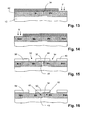
- implantation operations may optionally be supplemented by new implantations, on each side, to locally introduce even more P-type impurities to the right ( Figure 13 drawn on a smaller scale than the previous figures 2 to 12) and of type N on the left ( Figure 14 ) at locations where electrical contacts are to be made with metal interconnects.
- the entire substrate is then covered with an insulating layer 50 which is etched ( Figure 15 ) to remove it from both sides of the insulating strip 40 which follows the path of the guide.
- the insulating layer 50 thus remains above the actual guide, that is to say above the slot constituted by the insulating or semi-insulating wall 34 and above the silicon zones along the slit of the slit. and other of it; but the layer 50 is removed and stripped the silicon on two sidebands 52 and 54 on either side of the guide.
- the slot guide is then defined by the slot 34 of insulating or semi-insulating material, the two silicon areas 60 and 62 located on either side of the slot and delimited by the etching of part of the depth of the slot. silicon, the insulating zone 40 located below the slot and these two areas of silicon, and the oxide layer 50 above the slot and the two silicon areas.
- the depth of attack of silicon is for example about one third of the height. It must be sufficient to confine the optical waves in the path of the slotted guide even if this path has bifurcation angles or curvatures, but not too great not to induce excessive optical losses (and not to create in operating an electrical resistance too high access to the areas 60 and 62).
- annealing can be carried out which allows the diffusion of impurities P and N implanted previously (as explained with reference to Figures 11 to 14 ).
Landscapes
- Physics & Mathematics (AREA)
- Engineering & Computer Science (AREA)
- Optics & Photonics (AREA)
- General Physics & Mathematics (AREA)
- Microelectronics & Electronic Packaging (AREA)
- Chemical & Material Sciences (AREA)
- Nanotechnology (AREA)
- Nonlinear Science (AREA)
- Life Sciences & Earth Sciences (AREA)
- Biophysics (AREA)
- Crystallography & Structural Chemistry (AREA)
- Optical Integrated Circuits (AREA)
Description
- L'invention concerne la fabrication de circuits de photonique sur silicium. La photonique sur silicium est le domaine des composants optoélectroniques capables de manipuler des informations sous forme optique, ces composants étant réalisés dans des technologies analogues à celles qui sont utilisées pour des circuits intégrés d'électronique. Ces composants optoélectroniques utilisent le même matériau de base, à savoir le silicium, que les composants purement électroniques. Ce sont principalement des modulateurs optiques, démodulateurs, et circuits optiques non linéaires. Ils peuvent être associés, sur un même substrat, à des circuits électroniques qui servent à les commander ou qui servent à recueillir et traiter électroniquement les signaux électriques issus de la conversion des signaux optiques dans des photodétecteurs. Des sources de lumière peuvent également être intégrées sur le même substrat. Le brevet
US6 845 198 décrit un modulateur optique sur silicium. - Un des concepts de base consiste à former dans le silicium des guides de lumière de dimension très faibles (quelques centaines de nanomètres de section) soumis à l'influence de concentrations variables de porteurs (électrons ou trous) dans le silicium. Par la modulation électrique de la concentration des porteurs, on peut agir sur l'indice de réfraction du milieu optique du guide ; on agit donc sur la vitesse de propagation de la lumière dans le guide.
- Par exemple, en modulant le temps de propagation de la lumière dans deux branches optiques distinctes, commandées séparément, on produit un déphasage entre les ondes optiques qui sortent des deux branches. En les faisant interférer, on convertit ce déphasage en une modulation d'amplitude. C'est le principe des interféromètres de Mach Zehnder.
- On a imaginé notamment de réaliser des guides en silicium dits guides à fentes, comprenant deux murs de silicium dopé (à fort indice de réfraction) séparés par une fente remplie d'un milieu isolant, ou parfois semi-isolant, à faible indice de réfraction ; la lumière est confinée dans le guide du fait des discontinuité d'indice entre les murs de silicium et le matériau de la fente. Le confinement est d'autant meilleur que la fente est plus étroite et que la différence des indices est plus élevée. Les deux murs peuvent être dopés avec des impuretés de même type et le guide se comporte électriquement comme une capacité ; la tension aux bornes de la capacité crée des concentrations de charges électriques dans les murs de silicium ; les variations de concentrations (passives ou fonction d'une commande électrique) engendrent des variations d'indice de réfraction. Mais les murs de silicium peuvent aussi être dopés avec des impuretés de type opposé, et le guide se comporte alors comme une jonction PN ; les variations de tension aux bornes de la jonction créent aussi des accumulations ou déplétions de charges électriques agissant sur l'indice de réfraction donc sur la propagation de la lumière. L'isolant (ou semi-isolant) placé entre les deux murs de silicium constitue une barrière électrique évitant le transport de porteurs de charges entre les murs. L'article "Silicon Optical Modulators" de G.T. Reed, G. Mashanovich, F.Y. Gardes, et D.J. Thomson dans Nature Photonics, vol 4, Août 2010, pages 518-526, décrit des modulateurs optiques sur silicium utilisant des structures de guide à fente.
- Avec de tels guides à fente, on peut réaliser des commutateurs optiques, des sources de lumière, et des capteurs optiques.
- On a déjà proposé de réaliser de tels guides en creusant une fente dans une couche de silicium et en remplissant cette fente de matériau isolant ou semi-isolant. Mais ce procédé ne permet pas de faire des fentes très étroites et ayant une hauteur suffisante, car le remplissage ne se fait pas bien.
- On a également proposé, dans la publication de brevet
FR 2 907 916 - Cependant, le procédé décrit dans cette publication a l'inconvénient important de ne pas permettre une isolation électrique suffisante entre les deux murs de silicium ; ils sont en effet reliés à leur base du fait qu'ils reposent tous deux sur une même couche de silicium monocristallin. Même si cette couche est très peu dopée et très fine, elle n'est pas complètement isolante et des porteurs peuvent s'y déplacer, d'autant plus que la fente entre les deux murs est très étroite.
- La présente invention propose un procédé amélioré pour fabriquer un guide à fente, qui ne présente pas cet inconvénient et qui est facile à mettre en oeuvre indépendamment de la largeur souhaitée pour la fente.
- Le procédé selon l'invention est un procédé de fabrication d'un guide optique à fente sur silicium, comprenant le dépôt d'une fine couche de silicium monocristallin sur un substrat recouvert d'une couche enterrée isolante, et ultérieurement le dépôt uniforme d'une couche isolante ou semi-isolante sur la couche de silicium, le creusement sur toute l'épaisseur de cette couche isolante ou semi-isolante de deux ouvertures à flancs verticaux séparées par un intervalle étroit constituant un mur vertical isolant ou semi-isolant s'étendant le long d'un trajet qui est le trajet désiré pour le guide à fente, et la croissance épitaxiale de silicium monocristalllin dans les ouvertures, caractérisé en ce qu'avant le dépôt uniforme de la couche isolante ou semi-isolante, on effectue une oxydation thermique locale dans toute la profondeur de la fine couche de silicium monocristallin pour former une bande oxydée isolante s'étendant le long du trajet du mur vertical, sous celui-ci et de part et d'autre de celui-ci sur toute la longueur du trajet, de sorte que le mur vertical isolant qui sera ultérieurement formé ne soit pas adjacent à la fine couche de silicium monocristallin.
- Après l'étape d'oxydation de la fine couche de silicium monocristallin, on dépose la couche isolante ou semi-isolante et on la grave ; Puis on effectue la croissance épitaxiale de silicium sur toute la hauteur du mur vertical isolant ou semi-isolant, y compris au-dessus de la bande oxydée isolante et jusqu'à ce que le silicium vienne en contact avec le mur sur toute sa hauteur. Lors de cette croissance, le silicium recouvre non seulement la fine couche de silicium monocristallin mais aussi la bande oxydée jusque contre le mur vertical. Mais bien qu'à cet endroit il ne soit pas directement en contact avec la fine couche monocristalline il en prend cependant la structure monocristalline puisqu'il est tout proche de zones croissant de manière monocristalline au-dessus de la fine couche. On peut faire croître le silicium à une hauteur supérieure à celle du mur, et dans ce cas on effectue une étape de polissage mécanique et/ou chimique pour ajuster la hauteur du mur et du silicium.
- Avant d'effectuer la croissance monocristalline du silicium, on peut effectuer une étape de réduction de l'épaisseur du mur isolant ou semi-isolant ; cette réduction peut se faire par gravure chimique ou par gravure sèche isotrope.
- Le silicium qu'on fait croître est de préférence peu ou pas dopé. Il est dopé dans une étape postérieure au dépôt. De préférence, on dope le silicium avec une impureté de type N d'un côté du mur vertical et avec une impureté de type P de l'autre côté.
- D'autres caractéristiques et avantages de l'invention apparaîtront à la lecture de la description détaillée qui suit et qui est faite en référence aux dessins annexés dans lesquels :
- la
figure 1 représente en perspective un schéma de principe de la structure de guide à fente qu'on souhaite réaliser, pour former un déphaseur optique à diode ; - les
figures 2 à 9 représentent les étapes successives de fabrication du mur vertical isolant qui constituera la fente du guide à fente ; - les
figures 10 à 14 représentent les étapes de croissance du silicium qui encadre la fente, et le dopage du silicium ; - les
figures 15 et 16 représentent la fermeture supérieure du guide et la gravure du silicium qui le constitue ; - les
figures 17 à 19 représentent la formation de contacts électrique d'accès au guide pour la modulation de concentration de porteurs. - La structure de la
figure 1 est une figure de principe d'un guide à fente sur silicium, formé sur un substrat SOI, qu'on peut réaliser avec le procédé selon l'invention. Dans le cas représenté, le guide comprend une jonction NP avec une fente isolante ou semi-isolante séparant la région N de la région P ; cependant, on pourrait aussi envisager en restant dans le cadre de l'invention, un guide sans jonction qui comprendrait alors, de chaque côté de la fente des régions de même type N ou P et non des régions de type opposé ; ce guide se comporterait comme une capacité pure, les variations de charges des armatures de la capacité induisant des variations d'indice optique dans le guide, donc des variations de retard de phase optique. L'avantage des guides à diode est cependant que les variations de potentiel appliquées aux bornes de la jonction induisent des variations de concentration par déplétion de porteurs majoritaires, et cela sur les deux côtés de la fente ; le processus de déplétion est très rapide. Dans le cas où on a deux régions N ou deux régions P, l'action se fait d'un côté sur les porteurs majoritaires, et de l'autre sur les porteurs minoritaires, ce qui ralentit le processus de variation des concentrations de charges. On décrira la suite du procédé selon l'invention uniquement à propos d'un guide à fente à jonction PN. L'invention est applicable par ailleurs à des jonctions comportant du silicium intrinsèque en plus des zones dopées N et P (diodes PIN). - Le guide à fente comprend un substrat de silicium de type SOI. Il est composé d'un substrat de silicium 10 recouvert d'une couche isolante 12 en oxyde de silicium SiO2, elle-même recouverte d'une couche de silicium 14 dans laquelle sont formées une région 16 dopée de type N et une région 18 dopée de type P. Une fente 20 remplie de matériau isolant ou semi-isolant sépare la région N de la région P. La fente est recouverte d'une couche isolante 22. Le matériau isolant ou semi-isolant de la fente a un indice optique très inférieur à celui des murs de silicium dopé qui encadrent la fente. A titre d'exemple, le matériau de la fente est à base d'oxyde de silicium d'indice environ 1,5 alors que le silicium dopé a un indice de 3 à 4. La fente est très étroite (quelques dizaines de nanomètres) et sa hauteur est très supérieure à sa largeur (de 5 à 10 fois supérieure).
- Des contacts métalliques 24 et 26 peuvent être pris sur les régions N et P, ou sur des régions plus dopées N+ et P+ prolongeant les régions N et P respectivement. Ces contacts servent à commander la modulation de concentration de porteurs dans les régions N et P pour agir sur la vitesse de propagation de la lumière dans le guide à fente.
- Pour fabriquer une telle structure, on part d'un substrat de silicium sur isolant comprenant (
Figure 2 ) : un substrat de silicium 10 recouvert d'une couche isolante 12 de SiO2, sur laquelle on a fait croître une très fine couche de silicium monocristallin 30. L'épaisseur de cette couche 30 est de préférence inférieure à 100 nanomètres ; une couche de 30 à 60 nanomètres d'épaisseur est préférée. Cette couche est peu ou pas dopée (par exemple un taux d'impuretés d'environ 1015 atomes/cm3). Elle sert essentiellement de germe de croissance monocristalline pour une croissance ultérieure de silicium. Elle doit être suffisamment mince pour pouvoir être localement oxydée sans difficulté sur toute son épaisseur. - On dépose sur cette couche de silicium 30 une couche de masquage 32, de préférence en nitrure de silicium Si3N4 ; on grave la couche de masquage 32 par photolithographie pour définir une ouverture qui suit le trajet, dans le sens de la longueur, de la fente que l'on désire réaliser, et qui est plus large que cette fente. Par longueur de la fente on entend la dimension d'extension le long de la surface du substrat. Le trajet de la fente dans le sens de la longueur peut être court ou long, droit ou brisé ou courbe.
- Par exemple, si la fente doit avoir une largeur de 30 nanomètres, on ouvre la couche de masquage sur 100 ou 200 nanomètres de large. La
figure 3 représente cette étape ; on notera que l'échelle est dilatée dans le sens de la hauteur par rapport à l'échelle de lafigure 2 , pour mieux faire apparaître la couche 30. Le rôle de la couche de masquage 32 est de protéger le silicium de la couche 30 contre une oxydation thermique. - On effectue alors une étape d'oxydation thermique du silicium 30 à haute température. Le silicium s'oxyde complètement et devient de l'oxyde SiO2 là où il n'est pas recouvert de la couche de masquage 32 (
Figure 4 ). La couche de silicium 30 est donc maintenant séparée en deux parties par une bande oxydée 40 suivant le trajet désiré pour la fente, de sorte qu'on pourra ultérieurement appliquer des potentiels différents aux portions de silicium situées de part et d'autre de la zone isolante ainsi formée. - On conserve la couche de masquage et on recouvre le substrat (
Figure 5 ) d'une couche 34 de la matière isolante ou semi-isolante qui composera le matériau de la fente. Cette matière peut être de l'oxyde de silicium stoechiométrique SiO2, ou encore de l'oxyde de silicium non stoechiométrique SiOx. Si l'oxyde est non stoechiométrique avec x<2, un recuit de la couche produira des inclusions locales de cristaux de silicium noyés dans de l'oxyde isolant SiO2, aboutissant à une couche semi-isolante. La hauteur de la couche 34 est de plusieurs centaines de nanomètres par exemple 500 nanomètres. Elle est largement supérieure à la largeur désirée pour la fente du guide, en ce sens que le rapport hauteur/largeur est d'au moins 2, et de préférence compris entre 5 et 10. - Dans certains cas, la couche isolante ou semi-isolante pourrait aussi être en matériau de type III-V (AsGa ou InP) pour réaliser des sources de lumière. Dans ce cas, cette couche serait collée plutôt que déposée in situ.
- On dépose alors (
figure 6 ) une nouvelle couche de masquage 36 que l'on grave par photolithographie pour définir une bande qui suit le tracé, dans le sens de la longueur, de la fente à réaliser. La largeur de cette bande peut être la largeur finale de la fente souhaitée, mais si la photolithographie ne permet pas de faire une largeur aussi faible (typiquement 30 nanomètres), on formera une bande de couche 36 plus large, par exemple 100 nanomètres de large, et on effectuera ultérieurement une réduction de largeur de fente comme on l'expliquera plus loin. Le masque 36 est de préférence en nitrure de silicium, ou en carbure de silicium, ou un métal ou une résine, résistant aux produits d'attaque de la couche 34 de SiO2 ou SiOx. - On creuse la couche 34 (
figure 7 ) par gravure anisotrope verticale ; l'attaque est arrêtée lorsqu'on atteint la couche 32 située au-dessous de la couche 34. Les ouvertures formées pendant cette étape sont à flancs verticaux. On forme simultanément deux ouvertures très proches l'une de l'autre, respectivement à gauche et à droite du trajet désiré pour la fente. Il subsiste un mur vertical 34 situé au-dessus de la bande 40 qui a été oxydée à l'étape de lafigure 4 . - On élimine par voie chimique ou par gravure sèche isotrope à la fois la couche 32 et la couche 36 (
Figure 8 ). Cette opération est particulièrement simple si ces deux couches sont en nitrure de silicium. Cette élimination est faite avec un produit de gravure qui n'attaque pas la couche 34 d'oxyde de silicium. Il subsiste alors un mur vertical de couche isolante ou semi-isolante 34, reposant sur zone isolante 40 plus large que le mur ; le mur et la zone isolante 40 suivent le trajet désiré pour le guide à fente à la surface du substrat, sur toute la longueur de ce trajet. A l'extérieur de la zone isolante 40, on trouve le silicium dénudé de la couche originale 30 ; ce silicium ne vient pas en contact avec le mur isolant 34. - On peut alors, si nécessaire, procéder à une attaque anisotrope du mur vertical du matériau servant à constituer la fente. Cette attaque sert à amincir encore le mur, pour le faire passer par exemple d'une largeur de 100 nanomètres à une largeur de 30 à 50 nanomètres (
Figure 9 ). Cette gravure isotrope peut réduire la hauteur de l'oxyde de silicium sur lequel repose le mur, mais cela n'a pas d'inconvénient. Alternativement, dans le cas où le mur est fait dans un composé SiOx non stoechiométrique, on peut effectuer la réduction de largeur du mur en deux étapes qui sont d'abord une oxydation du composé SiOx sur une certaine profondeur (par exemple 30 nanomètres), formant un oxyde stoechiométrique, puis une élimination sélective de l'oxyde stoechiométrique par un produit qui n'attaque pas ou peu l'oxyde non stoechiométrique. - On fait croître alors une couche épitaxiale de silicium monocristallin 42 sur une épaisseur correspondant au moins à la hauteur du mur isolant ou semi-isolant 34. La croissance épitaxiale se fait en hauteur et latéralement. Elle recouvre les zones isolantes latérales 40 de part et d'autre du mur et peut recouvrir aussi le mur. Dans le cas où l'épaisseur de silicium est telle que le mur est recouvert par le silicium, on procède ensuite à une étape de polissage mécanique et/ou chimique (CMP) pour ramener le haut du silicium et le haut du mur dans un même surface plane, à une hauteur désirée (
figure 10 ). - Le silicium qu'on fait croître à ce stade est du silicium intrinsèque et peu dopé (par exemple aux alentours de 1015 atomes par centimètre cube), dont on complète ensuite le dopage P ou N en fonction des besoins.
- A la
figure 11 on effectue un dopage de la zone P en masquant le substrat par un masque de résine 44 sur toute la partie gauche de la figure, incluant le mur isolant ou semi-isolant 34. Le dopage est fait par implantation ionique ; il sera suivi ultérieurement d'un recuit faisant diffuser les impuretés implantées jusqu'à proximité immédiate du mur isolant 34. - A la
figure 12 , on effectue une opération similaire à celle de lafigure 11 mais inversée, pour implanter une impureté de type N de l'autre côté du mur 34. Un masque de résine 46 remplace à cet effet le masque 44 pour protéger la partie droite de la figure et dénuder le silicium sur la partie gauche. Là encore le recuit ultérieur fera diffuser les impuretés implantées jusqu'à proximité du mur 34. - On peut compléter facultativement ces opérations d'implantation par de nouvelles implantations, de chaque côté, pour introduire localement encore plus d'impuretés de type P à droite (
Figure 13 , dessinée à plus petite échelle que les figures précédentes 2 à 12) et de type N à gauche (Figure 14 ) à des endroits où on veut établir des contacts électriques avec des interconnexions métalliques. - On recouvre ensuite l'ensemble du substrat d'une couche isolante 50 que l'on grave (
Figure 15 ) pour l'enlever de part et d'autre de la bande isolante 40 qui suit le trajet du guide. La couche isolante 50 subsiste donc au-dessus du guide proprement dit, c'est-à-dire au-dessus de la fente constituée par le mur isolant ou semi-isolant 34 et au-dessus de zones de silicium longeant la fente de part et d'autre de celle-ci ; mais la couche 50 est enlevée et dénude le silicium sur deux bandes latérales 52 et 54 de part et d'autre du guide. - On attaque ensuite le silicium (
Figure 16 ) dans les zones 52 et 54 non protégées par l'oxyde 50 et on enlève une partie de la hauteur du silicium de type N et du silicium de type P. - Le guide à fente est alors défini par la fente 34 en matériau isolant ou semi-isolant, les deux zones de silicium 60 et 62 situées de part et d'autre de la fente et délimitées par la gravure d'une partie de la profondeur du silicium, la zone isolante 40 située au-dessous de la fente et de ces deux zones de silicium, et la couche d'oxyde 50 au-dessus de la fente et des deux zones de silicium.
- La profondeur d'attaque du silicium est par exemple d'environ un tiers de la hauteur. Elle doit être suffisante pour bien confiner les ondes optiques sur le trajet du guide à fente même si ce trajet présente des angles de bifurcation ou des courbures, mais pas trop grande pour ne pas induire de pertes optiques trop élevées (et pour ne pas créer en fonctionnement une résistance électrique d'accès trop importante vers les zones 60 et 62).
- On peut effectuer à ce stade le recuit qui permet la diffusion des impuretés P et N implantées auparavant (comme expliqué en référence aux
figures 11 à 14 ). - On recouvre alors l'ensemble du substrat d'une nouvelle couche isolante 66 (
Figure 17 , dessinée à plus petite échelle que les figures précédentes 13 à 16). On ouvre cette couche 66 (Figure 18 ) pour dénuder le silicium à l'endroit où on avait effectué une implantation supplémentaire N++ et P++ destinée à la prise de contact. Enfin on fait un dépôt de couche métallique (aluminium par exemple) et on grave cette couche pour établir les interconnexions nécessaires et les contacts 70 et 72 d'accès aux deux côtés du guide à fente (Figure 19 ).
Claims (8)
- Procédé de fabrication d'un guide optique à fente sur silicium, comprenant le dépôt d'une fine couche de silicium monocristallin (30) sur un substrat (10) recouvert d'une couche enterrée isolante (12), et ultérieurement le dépôt uniforme d'une couche isolante ou semi-isolante (34) sur la couche de silicium, le creusement sur toute l'épaisseur de cette couche isolante ou semi-isolante de deux ouvertures à flancs verticaux séparées par un intervalle étroit constituant un mur vertical isolant ou semi-isolant s'étendant le long d'un trajet qui est le trajet désiré pour le guide à fente, et la croissance épitaxiale de silicium monocristalilin (42) dans les ouvertures, caractérisé en ce qu'avant le dépôt uniforme de la couche isolante ou semi-isolante, on effectue une oxydation thermique locale dans toute la profondeur de la fine couche de silicium monocristallin (30) pour former une bande oxydée isolante s'étendant le long du trajet du mur vertical, sous celui-ci et de part et d'autre de celui-ci sur toute la longueur du trajet, de sorte que le mur vertical isolant qui sera ultérieurement formé ne soit pas adjacent à la fine couche de silicium monocristallin.
- Procédé de fabrication selon la revendication 1, caractérisé en ce que, après l'étape d'oxydation de la fine couche de silicium monocristallin, on dépose la couche isolante ou semi-isolante et on la grave.
- Procédé selon la revendication 2, caractérisé en ce qu'on effectue la croissance épitaxiale de silicium jusqu'à ce que le silicium vienne en contact avec le mur y compris au-dessus de la bande oxydée isolante.
- Procédé selon la revendication 1, caractérisé en ce qu'on effectue une étape de polissage mécanique et/ou chimique pour ajuster la hauteur du silicium et du mur.
- Procédé selon l'une des revendications 1 à 4, caractérisé en ce que, avant d'effectuer la croissance monocristalline du silicium, on effectue une étape de réduction de l'épaisseur du mur isolant ou semi-isolant.
- Procédé selon l'une des revendications 1 à 5, caractérisé en ce qu'après la croissance épitaxiale du silicium, on effectue un dopage de ce dernier.
- Procédé selon la revendication 6, caractérisé en ce qu'on dope le silicium avec une impureté de type N d'un côté du mur et avec une impureté de type P de l'autre côté.
- Procédé selon la revendication 6, caractérisé en ce qu'on dope le silicium avec une impureté de même type, N ou P, de chaque côté du mur.
Applications Claiming Priority (1)
| Application Number | Priority Date | Filing Date | Title |
|---|---|---|---|
| FR1060438A FR2968776B1 (fr) | 2010-12-13 | 2010-12-13 | Procédé pour réaliser un guide optique a fente sur silicium |
Publications (2)
| Publication Number | Publication Date |
|---|---|
| EP2463695A1 EP2463695A1 (fr) | 2012-06-13 |
| EP2463695B1 true EP2463695B1 (fr) | 2015-08-05 |
Family
ID=44276099
Family Applications (1)
| Application Number | Title | Priority Date | Filing Date |
|---|---|---|---|
| EP11192997.2A Not-in-force EP2463695B1 (fr) | 2010-12-13 | 2011-12-12 | Procédé pour réaliser un guide optique à fente sur silicium |
Country Status (3)
| Country | Link |
|---|---|
| US (1) | US8415185B2 (fr) |
| EP (1) | EP2463695B1 (fr) |
| FR (1) | FR2968776B1 (fr) |
Families Citing this family (9)
| Publication number | Priority date | Publication date | Assignee | Title |
|---|---|---|---|---|
| US8891913B1 (en) * | 2012-07-11 | 2014-11-18 | Aurrion, Inc. | Heterogeneous semiconductor photonic integrated circuit with multiple offset heights |
| FR3024781B1 (fr) * | 2014-08-11 | 2017-12-15 | Commissariat Energie Atomique | Procede de fabrication d'un guide optique |
| FR3034879B1 (fr) | 2015-04-13 | 2018-06-22 | Commissariat A L'energie Atomique Et Aux Energies Alternatives | Guide d'onde pour modulateur electro-optique de type capacitif. |
| EP3506002B1 (fr) * | 2017-12-29 | 2022-06-08 | IHP GmbH - Innovations for High Performance Microelectronics / Leibniz-Institut für innovative Mikroelektronik | Dispositif électro-optique |
| GB201815847D0 (en) * | 2018-09-28 | 2018-11-14 | Cambridge Entpr Ltd | Photodetector |
| JP2020080389A (ja) * | 2018-11-14 | 2020-05-28 | 日本電信電話株式会社 | ナノワイヤ光デバイス |
| CN111916347B (zh) * | 2020-08-13 | 2023-03-21 | 中国电子科技集团公司第四十四研究所 | 一种用于soi片的磷扩散掺杂方法 |
| US11869991B2 (en) * | 2020-09-18 | 2024-01-09 | Taiwan Semiconductor Manufacturing Company Limited | Semiconductor device and method of making |
| WO2025198653A1 (fr) * | 2023-11-02 | 2025-09-25 | President And Fellows Of Harvard College | Systèmes quantiques optiques manipulés électriquement |
Family Cites Families (12)
| Publication number | Priority date | Publication date | Assignee | Title |
|---|---|---|---|---|
| US6000947A (en) * | 1994-04-12 | 1999-12-14 | The Board Of Trustees Of The Leland Stanford, Jr. | Method of fabricating transistor or other electronic device using scanning probe microscope |
| US6845198B2 (en) * | 2003-03-25 | 2005-01-18 | Sioptical, Inc. | High-speed silicon-based electro-optic modulator |
| JP4533041B2 (ja) * | 2003-08-28 | 2010-08-25 | キヤノン株式会社 | 光素子の製造方法 |
| US7601551B2 (en) * | 2005-09-09 | 2009-10-13 | Denso Corporation | Method for manufacturing optical device |
| FR2907916B1 (fr) * | 2006-10-31 | 2009-01-23 | Commissariat Energie Atomique | Nouvelle structure de guide a fente |
| FR2907917B1 (fr) * | 2006-10-31 | 2009-01-23 | Commissariat Energie Atomique | Nouvelle structure de guide a fente |
| JP5117156B2 (ja) * | 2007-10-05 | 2013-01-09 | 株式会社日立製作所 | 半導体装置 |
| US7790495B2 (en) * | 2007-10-26 | 2010-09-07 | International Business Machines Corporation | Optoelectronic device with germanium photodetector |
| FR2937427B1 (fr) * | 2008-10-17 | 2011-03-04 | Commissariat Energie Atomique | Procede de fabrication d'un modulateur electro-optique lateral sur silicium a zones implantees auto-alignees |
| WO2010055750A1 (fr) * | 2008-11-12 | 2010-05-20 | 株式会社日立製作所 | Élément émetteur de lumière, élément récepteur de lumière et procédé de fabrication de l'élément récepteur de lumière |
| US8909021B2 (en) * | 2010-02-01 | 2014-12-09 | Hitachi, Ltd. | Semiconductor optical device |
| CN102315170B (zh) * | 2011-05-26 | 2013-07-31 | 北京大学 | 一种基于湿法腐蚀制备硅纳米线场效应晶体管的方法 |
-
2010
- 2010-12-13 FR FR1060438A patent/FR2968776B1/fr not_active Expired - Fee Related
-
2011
- 2011-12-12 EP EP11192997.2A patent/EP2463695B1/fr not_active Not-in-force
- 2011-12-13 US US13/324,721 patent/US8415185B2/en not_active Expired - Fee Related
Also Published As
| Publication number | Publication date |
|---|---|
| FR2968776B1 (fr) | 2012-12-28 |
| US8415185B2 (en) | 2013-04-09 |
| US20120149178A1 (en) | 2012-06-14 |
| EP2463695A1 (fr) | 2012-06-13 |
| FR2968776A1 (fr) | 2012-06-15 |
Similar Documents
| Publication | Publication Date | Title |
|---|---|---|
| EP2463695B1 (fr) | Procédé pour réaliser un guide optique à fente sur silicium | |
| EP3716345B1 (fr) | Procédé de fabrication d'une puce photonique comprenant une photodiode sacm-apd couplée optiquement à un guide d'ondes intégré | |
| EP1730560B1 (fr) | Modulateur optoelectronique haute frequence integre sur silicium | |
| EP1837916A1 (fr) | Procédé de réalisation d'un transistor à canal comprenant du germanium | |
| EP2610915A1 (fr) | Transistor et procédé de fabrication d'un transistor | |
| FR2860919A1 (fr) | Structures et procedes de fabrication de regions semiconductrices sur isolant | |
| EP3266079A1 (fr) | Laser germanium sur silicium en technologie cmos | |
| FR3002079A1 (fr) | Procede de fabrication d'un transistor | |
| FR2810792A1 (fr) | Transistor mos vertical a grille enterree et procede de fabrication de celui-ci | |
| FR2693314A1 (fr) | Transistor JFET vertical à mode de fonctionnement bipolaire optimisé et procédé de fabrication correspondant. | |
| FR2907916A1 (fr) | Nouvelle structure de guide a fente | |
| US10983411B2 (en) | Metal-oxide-semiconductor (MOS) optical modulator and method of manufacturing same | |
| EP3081983B1 (fr) | Guide d'onde pour modulateur electro-optique de type capacitif | |
| EP4088312B1 (fr) | Procédé de fabrication d'une structure de type semi-conducteur sur isolant pour applications radiofréquences | |
| EP3767376B1 (fr) | Modulateur optique capacitif | |
| FR3041116A1 (fr) | Modulateur electro-optique integre | |
| EP2628172A1 (fr) | Transistor a effet de champ sur ilot de materiau semiconducteur auto-assemble | |
| EP4492471B1 (fr) | Procédé de réalisation d'un état de contrainte dans une couche semi-conductrice | |
| EP4271165B1 (fr) | Procede de realisation d'un dispositif electronique a qubit(s) supraconducteur(s) incluant au moins un jofet | |
| EP3038160B1 (fr) | Transistor comprenant un canal mis sous contrainte en cisaillement et procede de fabrication | |
| EP2479785A1 (fr) | Dispositif à effet de champ muni d'une zone barrière de diffusion de dopants localisée et procédé de réalisation | |
| WO2006064124A1 (fr) | Modulateur a jonction capacitive, jonction capacitive et son procede de realisation | |
| FR2819637A1 (fr) | Circuit integre comportant un dispositif semiconducteur de type photodiode, et procede de fabrication | |
| FR2581801A1 (fr) | Procede de realisation de lasers a semiconducteurs a jonctions bloquantes assurant un confinement electrique | |
| FR2528234A1 (fr) | Dispositif semi-conducteur photoemetteur de type laser a guidage par gradient d'indice, et procede de realisation d'un tel dispositif |
Legal Events
| Date | Code | Title | Description |
|---|---|---|---|
| PUAI | Public reference made under article 153(3) epc to a published international application that has entered the european phase |
Free format text: ORIGINAL CODE: 0009012 |
|
| AK | Designated contracting states |
Kind code of ref document: A1 Designated state(s): AL AT BE BG CH CY CZ DE DK EE ES FI FR GB GR HR HU IE IS IT LI LT LU LV MC MK MT NL NO PL PT RO RS SE SI SK SM TR |
|
| AX | Request for extension of the european patent |
Extension state: BA ME |
|
| 17P | Request for examination filed |
Effective date: 20121127 |
|
| RAP1 | Party data changed (applicant data changed or rights of an application transferred) |
Owner name: COMMISSARIAT A L'ENERGIE ATOMIQUE ET AUX ENERGIES Owner name: UNIVERSITE PARIS-SUD 11 Owner name: CENTRE NATIONAL DE LA RECHERCHE SCIENTIFIQUE Owner name: ALCATEL LUCENT |
|
| GRAP | Despatch of communication of intention to grant a patent |
Free format text: ORIGINAL CODE: EPIDOSNIGR1 |
|
| INTG | Intention to grant announced |
Effective date: 20141110 |
|
| GRAS | Grant fee paid |
Free format text: ORIGINAL CODE: EPIDOSNIGR3 |
|
| GRAA | (expected) grant |
Free format text: ORIGINAL CODE: 0009210 |
|
| AK | Designated contracting states |
Kind code of ref document: B1 Designated state(s): AL AT BE BG CH CY CZ DE DK EE ES FI FR GB GR HR HU IE IS IT LI LT LU LV MC MK MT NL NO PL PT RO RS SE SI SK SM TR |
|
| REG | Reference to a national code |
Ref country code: GB Ref legal event code: FG4D Free format text: NOT ENGLISH |
|
| REG | Reference to a national code |
Ref country code: CH Ref legal event code: EP |
|
| REG | Reference to a national code |
Ref country code: AT Ref legal event code: REF Ref document number: 741031 Country of ref document: AT Kind code of ref document: T Effective date: 20150815 |
|
| REG | Reference to a national code |
Ref country code: IE Ref legal event code: FG4D Free format text: LANGUAGE OF EP DOCUMENT: FRENCH |
|
| REG | Reference to a national code |
Ref country code: DE Ref legal event code: R096 Ref document number: 602011018417 Country of ref document: DE |
|
| REG | Reference to a national code |
Ref country code: AT Ref legal event code: MK05 Ref document number: 741031 Country of ref document: AT Kind code of ref document: T Effective date: 20150805 |
|
| REG | Reference to a national code |
Ref country code: FR Ref legal event code: PLFP Year of fee payment: 5 |
|
| REG | Reference to a national code |
Ref country code: LT Ref legal event code: MG4D |
|
| REG | Reference to a national code |
Ref country code: NL Ref legal event code: MP Effective date: 20150805 |
|
| PG25 | Lapsed in a contracting state [announced via postgrant information from national office to epo] |
Ref country code: GR Free format text: LAPSE BECAUSE OF FAILURE TO SUBMIT A TRANSLATION OF THE DESCRIPTION OR TO PAY THE FEE WITHIN THE PRESCRIBED TIME-LIMIT Effective date: 20151106 Ref country code: FI Free format text: LAPSE BECAUSE OF FAILURE TO SUBMIT A TRANSLATION OF THE DESCRIPTION OR TO PAY THE FEE WITHIN THE PRESCRIBED TIME-LIMIT Effective date: 20150805 Ref country code: LV Free format text: LAPSE BECAUSE OF FAILURE TO SUBMIT A TRANSLATION OF THE DESCRIPTION OR TO PAY THE FEE WITHIN THE PRESCRIBED TIME-LIMIT Effective date: 20150805 Ref country code: NO Free format text: LAPSE BECAUSE OF FAILURE TO SUBMIT A TRANSLATION OF THE DESCRIPTION OR TO PAY THE FEE WITHIN THE PRESCRIBED TIME-LIMIT Effective date: 20151105 Ref country code: LT Free format text: LAPSE BECAUSE OF FAILURE TO SUBMIT A TRANSLATION OF THE DESCRIPTION OR TO PAY THE FEE WITHIN THE PRESCRIBED TIME-LIMIT Effective date: 20150805 |
|
| PG25 | Lapsed in a contracting state [announced via postgrant information from national office to epo] |
Ref country code: RS Free format text: LAPSE BECAUSE OF FAILURE TO SUBMIT A TRANSLATION OF THE DESCRIPTION OR TO PAY THE FEE WITHIN THE PRESCRIBED TIME-LIMIT Effective date: 20150805 Ref country code: ES Free format text: LAPSE BECAUSE OF FAILURE TO SUBMIT A TRANSLATION OF THE DESCRIPTION OR TO PAY THE FEE WITHIN THE PRESCRIBED TIME-LIMIT Effective date: 20150805 Ref country code: AT Free format text: LAPSE BECAUSE OF FAILURE TO SUBMIT A TRANSLATION OF THE DESCRIPTION OR TO PAY THE FEE WITHIN THE PRESCRIBED TIME-LIMIT Effective date: 20150805 Ref country code: PT Free format text: LAPSE BECAUSE OF FAILURE TO SUBMIT A TRANSLATION OF THE DESCRIPTION OR TO PAY THE FEE WITHIN THE PRESCRIBED TIME-LIMIT Effective date: 20151207 Ref country code: IS Free format text: LAPSE BECAUSE OF FAILURE TO SUBMIT A TRANSLATION OF THE DESCRIPTION OR TO PAY THE FEE WITHIN THE PRESCRIBED TIME-LIMIT Effective date: 20151205 Ref country code: PL Free format text: LAPSE BECAUSE OF FAILURE TO SUBMIT A TRANSLATION OF THE DESCRIPTION OR TO PAY THE FEE WITHIN THE PRESCRIBED TIME-LIMIT Effective date: 20150805 Ref country code: SE Free format text: LAPSE BECAUSE OF FAILURE TO SUBMIT A TRANSLATION OF THE DESCRIPTION OR TO PAY THE FEE WITHIN THE PRESCRIBED TIME-LIMIT Effective date: 20150805 Ref country code: HR Free format text: LAPSE BECAUSE OF FAILURE TO SUBMIT A TRANSLATION OF THE DESCRIPTION OR TO PAY THE FEE WITHIN THE PRESCRIBED TIME-LIMIT Effective date: 20150805 |
|
| PG25 | Lapsed in a contracting state [announced via postgrant information from national office to epo] |
Ref country code: NL Free format text: LAPSE BECAUSE OF FAILURE TO SUBMIT A TRANSLATION OF THE DESCRIPTION OR TO PAY THE FEE WITHIN THE PRESCRIBED TIME-LIMIT Effective date: 20150805 |
|
| PG25 | Lapsed in a contracting state [announced via postgrant information from national office to epo] |
Ref country code: EE Free format text: LAPSE BECAUSE OF FAILURE TO SUBMIT A TRANSLATION OF THE DESCRIPTION OR TO PAY THE FEE WITHIN THE PRESCRIBED TIME-LIMIT Effective date: 20150805 Ref country code: DK Free format text: LAPSE BECAUSE OF FAILURE TO SUBMIT A TRANSLATION OF THE DESCRIPTION OR TO PAY THE FEE WITHIN THE PRESCRIBED TIME-LIMIT Effective date: 20150805 Ref country code: CZ Free format text: LAPSE BECAUSE OF FAILURE TO SUBMIT A TRANSLATION OF THE DESCRIPTION OR TO PAY THE FEE WITHIN THE PRESCRIBED TIME-LIMIT Effective date: 20150805 Ref country code: IT Free format text: LAPSE BECAUSE OF FAILURE TO SUBMIT A TRANSLATION OF THE DESCRIPTION OR TO PAY THE FEE WITHIN THE PRESCRIBED TIME-LIMIT Effective date: 20150805 Ref country code: SK Free format text: LAPSE BECAUSE OF FAILURE TO SUBMIT A TRANSLATION OF THE DESCRIPTION OR TO PAY THE FEE WITHIN THE PRESCRIBED TIME-LIMIT Effective date: 20150805 |
|
| REG | Reference to a national code |
Ref country code: DE Ref legal event code: R097 Ref document number: 602011018417 Country of ref document: DE |
|
| PG25 | Lapsed in a contracting state [announced via postgrant information from national office to epo] |
Ref country code: BE Free format text: LAPSE BECAUSE OF NON-PAYMENT OF DUE FEES Effective date: 20151231 Ref country code: RO Free format text: LAPSE BECAUSE OF FAILURE TO SUBMIT A TRANSLATION OF THE DESCRIPTION OR TO PAY THE FEE WITHIN THE PRESCRIBED TIME-LIMIT Effective date: 20150805 |
|
| PLBE | No opposition filed within time limit |
Free format text: ORIGINAL CODE: 0009261 |
|
| STAA | Information on the status of an ep patent application or granted ep patent |
Free format text: STATUS: NO OPPOSITION FILED WITHIN TIME LIMIT |
|
| 26N | No opposition filed |
Effective date: 20160509 |
|
| PG25 | Lapsed in a contracting state [announced via postgrant information from national office to epo] |
Ref country code: MC Free format text: LAPSE BECAUSE OF FAILURE TO SUBMIT A TRANSLATION OF THE DESCRIPTION OR TO PAY THE FEE WITHIN THE PRESCRIBED TIME-LIMIT Effective date: 20150805 Ref country code: LU Free format text: LAPSE BECAUSE OF FAILURE TO SUBMIT A TRANSLATION OF THE DESCRIPTION OR TO PAY THE FEE WITHIN THE PRESCRIBED TIME-LIMIT Effective date: 20151212 |
|
| REG | Reference to a national code |
Ref country code: CH Ref legal event code: PL |
|
| PG25 | Lapsed in a contracting state [announced via postgrant information from national office to epo] |
Ref country code: SI Free format text: LAPSE BECAUSE OF FAILURE TO SUBMIT A TRANSLATION OF THE DESCRIPTION OR TO PAY THE FEE WITHIN THE PRESCRIBED TIME-LIMIT Effective date: 20150805 |
|
| REG | Reference to a national code |
Ref country code: IE Ref legal event code: MM4A |
|
| PG25 | Lapsed in a contracting state [announced via postgrant information from national office to epo] |
Ref country code: CH Free format text: LAPSE BECAUSE OF NON-PAYMENT OF DUE FEES Effective date: 20151231 Ref country code: LI Free format text: LAPSE BECAUSE OF NON-PAYMENT OF DUE FEES Effective date: 20151231 Ref country code: IE Free format text: LAPSE BECAUSE OF NON-PAYMENT OF DUE FEES Effective date: 20151212 |
|
| REG | Reference to a national code |
Ref country code: FR Ref legal event code: PLFP Year of fee payment: 6 |
|
| PGFP | Annual fee paid to national office [announced via postgrant information from national office to epo] |
Ref country code: GB Payment date: 20161221 Year of fee payment: 6 |
|
| PGFP | Annual fee paid to national office [announced via postgrant information from national office to epo] |
Ref country code: FR Payment date: 20161229 Year of fee payment: 6 |
|
| PGFP | Annual fee paid to national office [announced via postgrant information from national office to epo] |
Ref country code: DE Payment date: 20161221 Year of fee payment: 6 |
|
| PG25 | Lapsed in a contracting state [announced via postgrant information from national office to epo] |
Ref country code: SM Free format text: LAPSE BECAUSE OF FAILURE TO SUBMIT A TRANSLATION OF THE DESCRIPTION OR TO PAY THE FEE WITHIN THE PRESCRIBED TIME-LIMIT Effective date: 20150805 Ref country code: BG Free format text: LAPSE BECAUSE OF FAILURE TO SUBMIT A TRANSLATION OF THE DESCRIPTION OR TO PAY THE FEE WITHIN THE PRESCRIBED TIME-LIMIT Effective date: 20150805 Ref country code: HU Free format text: LAPSE BECAUSE OF FAILURE TO SUBMIT A TRANSLATION OF THE DESCRIPTION OR TO PAY THE FEE WITHIN THE PRESCRIBED TIME-LIMIT; INVALID AB INITIO Effective date: 20111212 |
|
| PG25 | Lapsed in a contracting state [announced via postgrant information from national office to epo] |
Ref country code: CY Free format text: LAPSE BECAUSE OF FAILURE TO SUBMIT A TRANSLATION OF THE DESCRIPTION OR TO PAY THE FEE WITHIN THE PRESCRIBED TIME-LIMIT Effective date: 20150805 |
|
| PG25 | Lapsed in a contracting state [announced via postgrant information from national office to epo] |
Ref country code: MT Free format text: LAPSE BECAUSE OF FAILURE TO SUBMIT A TRANSLATION OF THE DESCRIPTION OR TO PAY THE FEE WITHIN THE PRESCRIBED TIME-LIMIT Effective date: 20150805 Ref country code: TR Free format text: LAPSE BECAUSE OF FAILURE TO SUBMIT A TRANSLATION OF THE DESCRIPTION OR TO PAY THE FEE WITHIN THE PRESCRIBED TIME-LIMIT Effective date: 20150805 |
|
| PG25 | Lapsed in a contracting state [announced via postgrant information from national office to epo] |
Ref country code: MK Free format text: LAPSE BECAUSE OF FAILURE TO SUBMIT A TRANSLATION OF THE DESCRIPTION OR TO PAY THE FEE WITHIN THE PRESCRIBED TIME-LIMIT Effective date: 20150805 |
|
| REG | Reference to a national code |
Ref country code: DE Ref legal event code: R119 Ref document number: 602011018417 Country of ref document: DE |
|
| GBPC | Gb: european patent ceased through non-payment of renewal fee |
Effective date: 20171212 |
|
| REG | Reference to a national code |
Ref country code: FR Ref legal event code: ST Effective date: 20180831 |
|
| PG25 | Lapsed in a contracting state [announced via postgrant information from national office to epo] |
Ref country code: AL Free format text: LAPSE BECAUSE OF FAILURE TO SUBMIT A TRANSLATION OF THE DESCRIPTION OR TO PAY THE FEE WITHIN THE PRESCRIBED TIME-LIMIT Effective date: 20150805 Ref country code: DE Free format text: LAPSE BECAUSE OF NON-PAYMENT OF DUE FEES Effective date: 20180703 Ref country code: FR Free format text: LAPSE BECAUSE OF NON-PAYMENT OF DUE FEES Effective date: 20180102 |
|
| PG25 | Lapsed in a contracting state [announced via postgrant information from national office to epo] |
Ref country code: GB Free format text: LAPSE BECAUSE OF NON-PAYMENT OF DUE FEES Effective date: 20171212 |