EP2463780A1 - Fehlerbeseitigungsregister zum Halten von Prozessorkernen nach einem Reset oder dem Ausschalten - Google Patents
Fehlerbeseitigungsregister zum Halten von Prozessorkernen nach einem Reset oder dem Ausschalten Download PDFInfo
- Publication number
- EP2463780A1 EP2463780A1 EP11192311A EP11192311A EP2463780A1 EP 2463780 A1 EP2463780 A1 EP 2463780A1 EP 11192311 A EP11192311 A EP 11192311A EP 11192311 A EP11192311 A EP 11192311A EP 2463780 A1 EP2463780 A1 EP 2463780A1
- Authority
- EP
- European Patent Office
- Prior art keywords
- register
- halt
- debug
- reset
- responsive
- Prior art date
- Legal status (The legal status is an assumption and is not a legal conclusion. Google has not performed a legal analysis and makes no representation as to the accuracy of the status listed.)
- Withdrawn
Links
Images


Classifications
-
- G—PHYSICS
- G06—COMPUTING OR CALCULATING; COUNTING
- G06F—ELECTRIC DIGITAL DATA PROCESSING
- G06F11/00—Error detection; Error correction; Monitoring
- G06F11/22—Detection or location of defective computer hardware by testing during standby operation or during idle time, e.g. start-up testing
- G06F11/26—Functional testing
-
- G—PHYSICS
- G06—COMPUTING OR CALCULATING; COUNTING
- G06F—ELECTRIC DIGITAL DATA PROCESSING
- G06F11/00—Error detection; Error correction; Monitoring
- G06F11/36—Prevention of errors by analysis, debugging or testing of software
-
- G—PHYSICS
- G06—COMPUTING OR CALCULATING; COUNTING
- G06F—ELECTRIC DIGITAL DATA PROCESSING
- G06F11/00—Error detection; Error correction; Monitoring
- G06F11/36—Prevention of errors by analysis, debugging or testing of software
- G06F11/362—Debugging of software
- G06F11/3648—Debugging of software using additional hardware
- G06F11/3656—Debugging of software using additional hardware using a specific debug interface
-
- G—PHYSICS
- G01—MEASURING; TESTING
- G01R—MEASURING ELECTRIC VARIABLES; MEASURING MAGNETIC VARIABLES
- G01R31/00—Arrangements for testing electric properties; Arrangements for locating electric faults; Arrangements for electrical testing characterised by what is being tested not provided for elsewhere
- G01R31/28—Testing of electronic circuits, e.g. by signal tracer
- G01R31/317—Testing of digital circuits
- G01R31/3181—Functional testing
- G01R31/3183—Generation of test inputs, e.g. test vectors, patterns or sequences
Definitions
- This invention relates to integrated circuits, and more particularly, to mechanisms for debugging integrated circuits.
- Integrated circuits (ICs) and electronic assemblies are typically tested prior to shipping to a customer.
- One such testing mechanism developed for testing connections of ICs to printed circuit boards (PCB's) is known as boundary scan.
- Boundary scan testing is based on the IEEE 1149.1 Standard, which is commonly known as Joint Test Action Group (JTAG).
- JTAG Joint Test Action Group
- JTAG ports are sometimes used to access internal functional blocks of an IC for testing.
- the use of JTAG access ports has been further expanded for use in debugging IC designs as well as software designed to execute on such ICs.
- JTAG access ports have spurred further development in providing internal access to ICs.
- Many ICs now include a debug port (DP) having multiple JTAG access ports coupled to various internal components.
- the DP may also include one or more serial wire port (SWPs), memory access ports, and other types of ports that enable the accessing of internal IC functional blocks for debugging purposes.
- SWPs serial wire port
- Such access ports convey various signals to accessible functional blocks, including data signals and clock signals. For example, test input data, clock, and mode select signals may be conveyed to a functional block through a JTAG port, while test output data may be received through the JTAG port.
- Some ICs, such as processors may also include debug registers. Such debug registers may be programmed by executing processor code in a processor core.
- an IC includes a number of functional units accessible by an external debugger via a debug port.
- a power controller in the IC may put the functional unit to sleep and/or power down a functional unit.
- a first register Prior to or during the time that the functional unit is asleep/powered off, a first register may be programmed. Responsive to the programming of the first register and subsequent to putting the functional unit to sleep, a first signal may be asserted and provided to the functional unit. When power is restored to the functional unit or the functional unit is reset, operation of the functional unit may be halted prior to execution of instructions or other operations, responsive to the signal. Thus, the programming of the first register may signal the intention to halt the functional unit at the next reset, but the halt may be delayed until such reset occurs.
- the method and apparatus may also be used in conjunction with a reset operation.
- a debugger coupled to the debug port may program a second register to cause a reset of each of the functional units of the IC or selected functional units of the IC, with the exception of the debug port and associated debug circuitry.
- the first register may also be programmed, either by the debugger or responsive to the programming of the second register.
- the first register may be programmed prior to resetting the functional unit.
- the first signal may be received by a functional unit subsequent to initiating the reset. Responsive to receiving the first signal, the functional unit may halt operation upon exiting the reset.
- the IC may be a multi-core processor.
- Each of the processor cores may be coupled to a debug port via a debug bus.
- the debug port may provide access by an external debugger to each of the processor cores, and may also include a control unit operable to provide various control functions related to debugging operations.
- the IC may also include a power management unit (PMU) that may selectively put the processor cores to sleep and/or remove power from processor cores.
- PMU power management unit
- a group of registers accessible by the control unit may be coupled to the debug bus.
- the group of registers may include a register that may be programmed by the external debugger in conjunction with a reset of the IC or prior to the reset, or when the PMU removes power from one or more of the processor cores.
- the register may include a number of bit positions or bit position groups, each of which corresponds to a unique one of the processor cores. If a bit position or a bit position group corresponding to a particular processor core is programmed to halt the processor, a signal may be asserted to that processor core while the processor core is in reset. When the processor core exits the reset state, the processor core may detect the signal may. Responsive to detection of the signal, the processor core may halt operation prior to the execution of an initial instruction after the reset.
- the method and apparatus described herein may enable an external debugger to perform a number of debugging functions that may not otherwise be possible.
- an external debugger may program the registers discussed above to enable debugging of a boot-up sequence.
- the ability to halt operation before any instructions are executed may enable debugging to begin from a known reference point.
- providing the ability to program, prior to a reset, the debug registers to halt the processor after the next reset may simplify debugging while still permitting the halt of the processor prior to executing any instructions.
- the deferral of the halt until the reset may improve the ability to debug systems that may frequently put processors to sleep and awaken the processors (e.g. via a reset).
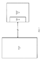
- Fig. 1 is a block diagram illustrating a connection of an external debugger to one embodiment of an IC for accessing internal components thereof.
- Fig. 2 is a block diagram of one embodiment of an IC.
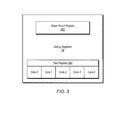
- Fig. 3 is a block diagram of one embodiment of a block of registers used in debugging an IC.
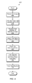
- Fig. 4 is a flow diagram of one embodiment of a method for halting operation of a functional block of an IC when restoring power.
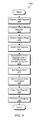
- Fig. 5 is a flow diagram of one embodiment of a method for performing a warm reset of an IC.
- Fig. 6 is a block diagram of one embodiment of an exemplary system.
- circuits, or other components may be described as “configured to” perform a task or tasks.
- “configured to” is a broad recitation of structure generally meaning “having circuitry that" performs the task or tasks during operation.
- the unit/circuit/component can be configured to perform the task even when the unit/circuit/component is not currently on.
- the circuitry that forms the structure corresponding to "configured to” may include hardware circuits.
- various units/circuits/components may be described as performing a task or tasks, for convenience in the description.
- Fig. 1 a block diagram illustrating a connection of an external debugger to one embodiment of an integrated circuit (IC) for accessing internal components thereof is shown.
- IC 10 is coupled to external debugger 5 via debug port 20.
- Debugger 5 may be a computer system or other type of test equipment operable to perform various types of tests of IC 10 and components thereof.
- debugger 5 may be used in debugging the design of IC 10 and software written to execute thereupon. As defined herein, debugging may include determining if any hardware errors are present within IC 10.
- Debugging may also include determining whether or not software correctly executes on IC 10.
- IC 10 may include a number of internal components that may be accessed by debugger 5 through debug port 20. Such components may include cores of a processor (e.g., execution cores), but may include other components as well (e.g., input/output units, etc.).
- Debugger 5 may provide test stimulus data to one or more components of IC 10 through debug port 20 and may initiate testing. Results of the test data may be received by debugger 5 through debug port 20.
- debugger 5 may also provide various control signals and programming information to control certain operations within IC 10 during debugging.
- debugger 5 may insert breakpoints to cause one or more components to stop operation and thus allow the state of such components to be retrieved for further analysis.
- Debugger 5 may also send control signals and programming information to IC 10 to cause certain components to be powered on, powered off, reset, or halted in various situations.
- Fig. 2 is a block diagram illustrating one embodiment of IC 10 in further detail.
- IC 10 includes a plurality of processor cores 25 that are coupled to debug port 20 via debug bus 22.
- IC 10 may be a heterogeneous (or asymmetric) multi-core processor in one embodiment, wherein various ones of the processor cores are different from each other.
- IC 10 may be a multi-core processor designed for use in a mobile platform, such as a smart phone, a laptop computer, or other mobile device, wherein each of the various processor cores 25 are dedicated to particular tasks.
- processor core 25 may be dedicated to performing audio-related tasks, another processor core 25 may be dedicated to graphics/video related tasks, while one or more other ones of the processor cores may be dedicated to executing instructions not explicitly related to audio and/or video tasks.
- IC 10 that implement a homogenous multi-core processor (i.e. where all processor cores are identical) are possible and contemplated.
- Other possible embodiments of IC 10 include application specific integrated circuits (ASICs) and other types of ICs.
- ASICs application specific integrated circuits
- IC 10 also includes a set of debug registers 26 coupled to debug bus 22.
- Debug registers 26 may include a number of different registers that may store information for use during debugging. Some of the registers may be used to trigger certain actions within IC 10 during debugging, while others may store information specifying certain conditions or parameters. Additional details of certain ones of registers 26 will be discussed below.
- Debug Port 20 in the embodiment shown may provide one or more physical connections for an external debugger (e.g., debugger 5 of Fig. 1 ) for performing debugging operations. These connections may include a Joint Test Action Group (JTAG) connection, a Serial Wire Debug (SWD) connection, and/or other types of connections that may be used with an external debugger. Debug Port 20 may also include various types of functional circuitry to support these connections.
- JTAG Joint Test Action Group
- SWD Serial Wire Debug
- debug port 20 includes logic circuitry which may provide certain control functions for controlling operation of itself and other circuitry of IC 10 during debugging. Some of these control functions may be specified by information stored in debug registers 26, and thus debug port 20 is coupled thereto via a bidirectional connection. Debug port 20 may thus write information into various ones of debug registers 26, and may also read information from the same. Furthermore, debug port 20 may also have the capability of clearing certain ones of registers 26.
- debug port 20 is configured to provide halt signals ('Halt') to each of processor cores 25. It is noted here while the signal path of the halt signal is depicted using a single line (for the sake of simplicity), unique instances of the halt signal may be provided to each of processor cores 25. When a halt signal is asserted to a given processor core 25, that core may halt operation prior to execution of a first instruction upon exiting a reset state or restoring power thereto. This may enable the inputting of test stimulus that allows the operation of a core or software executing thereon to be debugged beginning with a first instruction to be executed.
- IC 10 in the embodiment shown includes a power management unit (PMU) 29.
- PMU 29 is coupled to receive a supply voltage ('Vdd'), and may selectively put the processor core or cores 25 to sleep.
- a processor core that is asleep is not executing instructions.
- the core may be clock gated, the clock source (e.g. one or more phase locked loop (PLLs)) may be shut down, or the core may even be powered off in various implementations and/or levels of sleep.
- PLLs phase locked loop
- PMU 29 may put to sleep/power off those processor cores 25 that have been idle for a particular amount of time.
- PMU 29 may also awaken sleeping processors (restoring power to powered off processor cores 25 to enable their re-activation and/or resetting processor cores). In some embodiments, PMU 29 may control the voltage levels for providing power to processor cores 25, providing higher voltages when performance demand is greater and lower voltages when performance demand is lower.
- During debug operations may cause a reset of selected ones or all of processor cores 25 by asserting a reset signal and/or powering up a core to reawaking the core. If the debug registers 26 have been programmed with a deferred halt, the debug port 20 may assert the halt signal for the corresponding processor core(s) during power up/reset.
- Fig. 3 is a block diagram of one embodiment of a block of registers used in debugging an IC. More particularly, Fig. 3 illustrates particular ones of debug registers 26. It is noted however that additional registers not discussed here may also be included in debug registers 26.
- debug registers 26 includes a warm reset register 262.
- warm reset register 262 may cause a warm reset of IC 10 or portions thereof.
- the term 'warm reset' refers to a reset wherein each of processor cores 25, a subset of the processor cores 25, (and possibly other circuitry) is reset, but circuitry within the debug domain is not reset.
- debug port 20, debug registers 26, and other debug circuitry not explicitly discussed here may remain active while processor cores 25 and other non-debug circuitry is reset during the warm reset.
- PMU 29 may also be exempt from a reset during a warm reset operation, as such components may be used to initiate the reset.
- the warm reset may be indicated with as few bits as one. However, embodiments of a warm reset register 262 having a greater number of bits are possible and contemplated. For example, a bit per processor core 25 may be used to individually reset cores.
- halt register 264 is subdivided into a number of different sections, each of which corresponds to a particular one of processor cores 25. Each subsection may include one or more bits.
- the programming may be detected by circuitry within debug port 20. Responsive to initiation of a warm reset, or PMU 29 powering off the particular processor core 25, debug port 20 may assert a corresponding halt signal ('Halt'). Particularly, the halt signal may not be asserted immediately upon programming the register 264, but rather may be asserted during reset or after power down of the corresponding processor core 25.
- the halt signal may be received on a corresponding input of the particular processor core 25. Responsive to detecting the asserted halt signal upon exiting the reset state or otherwise having power restored thereto, the particular processor core 25 will halt operation prior to executing a first instruction. This may enable debugger 5 to begin testing or debugging of the particular processor core 25 from a known state, instead of a state that has been altered by the execution of instructions.
- each of the sections of halt register 264 may be programmed independently of one another. Accordingly, halt signals may be selectively asserted to some processor cores 25 and not asserted to others. This may in turn enable the halting of some processor cores 25 upon exiting a warm reset or having power restored thereto, while other processor cores 25 are allowed to being executing instructions (e.g., per a boot process or for resuming from a sleep state). In general, the ability to cause selected ones of processor cores 25 to halt upon exiting a reset or being powered on may provide an extra level of flexibility in performing debug operations. Furthermore, if desired, all sections of halt register 264 may be programmed in some instances to cause all processor cores 25 to halt upon exiting reset or otherwise having power restored thereto.
- Fig. 4 is a flow diagram of one embodiment of a method for halting operation of a functional block of an IC when restoring power.
- Method 400 will be discussed below with reference to the hardware embodiments discussed above. However, it is noted that method 400 may be used with other hardware embodiments not discussed herein.
- Method 400 begins with the powering off of one or more processor cores 25 (block 405).
- the powering off of the processor core(s) 25 may occur during the performance of debugging operation.
- PMU 29 powers off the processor core(s) 25, it may provide an indication to debug port 20 (block 410).
- the indication received by debug port 20 may be relayed to debugger 5, which may take action responsive thereto, such as programming other registers.
- halt register 264 may be programmed for at least one of the processor core(s) 25 that is powered off (block 415). Alternatively, the halt register 264 may be programmed prior to the power down, and the debug port 20 may delay assertion of the halt signal until the power down occurs.
- halt register 264 may be detected by debug port 201. Responsive to detecting the programming of halt register 264 and the powering down of the processor core 25, debug port 20 may assert and provide halt signals to the processor core(s) 25 corresponding to the programmed sections of halt register 264 (block 420).
- PMU 29 may re-apply power to these core(s) (block 425).
- the processor core(s) 25 receiving a respective halt signal may halt operation prior to execution of a first instruction (block 430). Halting the processor core(s) 25 before any instructions are executed may preserve an initial state present when power is initially applied. This may in turn allow debugger 5 to control or monitor the state of a given processor core 25 from its beginning of operation. This can be useful in different ways, such as when debugging a boot-up sequence.
- the halt register may be cleared.
- Fig. 5 is a flow diagram of one embodiment of a method for performing a warm reset of an IC or a particular processor core 25.
- method 500 is discussed herein with reference to the various hardware embodiments discussed in reference to Figs. 1-3 . However, it is noted that method 500 may be used with other hardware embodiments not explicitly discussed herein.
- Method 500 begins with debugger 5 programming warm reset register 262 and one or more sections of halt register 264 (blocks 504 and 505).
- the halt register 264 may be programmed at any point prior to programming the warm reset register 262.
- Debug port 20 may also provide an indication to PMU 29 of the programming of the warm reset register, thereby causing the performance of a warm reset (block 515).
- Debug port 20 may assert and provide halt signals to the processor core(s) 25 corresponding to the programmed section(s) of halt register 264 responsive to the warm reset (block 515).
- components that are not part of the debug domain may be reset. For example, in IC 10 of Figs.
- each of processor cores 25 may be reset during a warm reset, as well as other components that are not explicitly shown (e.g., input/output circuitry). However, during the warm reset, circuitry of the debug domain, including debug port 20, registers 26, and any other circuitry of the debug domain not explicitly shown or discussed here may be exempt from the reset. PMU 29 may also be exempt from the reset during a warm reset. In some embodiments, PMU 29 may actually initiate the warm reset.
- the reset state may be held for a certain number of cycles of a clock signal of IC 10 subsequent to its initiation. After the certain number of clock cycles has completed, warm reset register 262 may be cleared (block 520). In some embodiments, clearing of warm reset register 262 may be accomplished in one embodiment by debugger 5 writing a value of '0' to the register. In another embodiment, warm reset register 262 may include a self-timer that causes the register to be cleared once the predetermined number of clock cycles has elapsed.
- those components subject to the reset may exit the reset state (block 525).
- the processor core(s) 25 receiving an asserted halt signal may halt operation prior to the execution of a first instruction (block 530).
- the processor cores 25 for which a halt signal was asserted may receive power but may retain a state equivalent to that of being powered on with no instructions having been executed.
- halt register 264 may be cleared (block 535). Thereafter, debugging operations may begin (block 540).
- the system 150 includes at least one instance of an IC 10 (from Fig. 1 ) coupled to one or more peripherals 154 and an external memory 158.
- a power supply 156 is also provided which supplies the supply voltages to the IC 10 as well as one or more supply voltages to the memory 158 and/or the peripherals 154.
- more than one instance of the IC 10 may be included (and more than one external memory 158 may be included as well).
- the peripherals 154 may include any desired circuitry, depending on the type of system 150.
- the system 150 may be a mobile device (e.g. personal digital assistant (PDA), smart phone, etc.) and the peripherals 154 may include devices for various types of wireless communication, such as wifi, Bluetooth, cellular, global positioning system, etc.
- the peripherals 154 may also include additional storage, including RAM storage, solid state storage, or disk storage.
- the peripherals 154 may include user interface devices such as a display screen, including touch display screens or multitouch display screens, keyboard or other input devices, microphones, speakers, etc.
- the system 150 may be any type of computing system (e.g. desktop personal computer, laptop, workstation, net top etc.).
- the external memory 158 may include any type of memory.
- the external memory 158 may be SRAM, dynamic RAM (DRAM) such as synchronous DRAM (SDRAM), double data rate (DDR, DDR2, DDR3, etc.) SDRAM, RAMBUS DRAM, etc.
- DRAM dynamic RAM
- the external memory 158 may include one or more memory modules to which the memory devices are mounted, such as single inline memory modules (SIMMs), dual inline memory modules (DIMMs), etc.
Landscapes
- Engineering & Computer Science (AREA)
- Theoretical Computer Science (AREA)
- General Engineering & Computer Science (AREA)
- Computer Hardware Design (AREA)
- Physics & Mathematics (AREA)
- General Physics & Mathematics (AREA)
- Quality & Reliability (AREA)
- Debugging And Monitoring (AREA)
- Microcomputers (AREA)
Applications Claiming Priority (1)
| Application Number | Priority Date | Filing Date | Title |
|---|---|---|---|
| US12/963,975 US8402314B2 (en) | 2010-12-09 | 2010-12-09 | Debug registers for halting processor cores after reset or power off |
Publications (1)
| Publication Number | Publication Date |
|---|---|
| EP2463780A1 true EP2463780A1 (de) | 2012-06-13 |
Family
ID=45440124
Family Applications (1)
| Application Number | Title | Priority Date | Filing Date |
|---|---|---|---|
| EP11192311A Withdrawn EP2463780A1 (de) | 2010-12-09 | 2011-12-07 | Fehlerbeseitigungsregister zum Halten von Prozessorkernen nach einem Reset oder dem Ausschalten |
Country Status (5)
| Country | Link |
|---|---|
| US (2) | US8402314B2 (de) |
| EP (1) | EP2463780A1 (de) |
| KR (1) | KR101394850B1 (de) |
| TW (1) | TWI450078B (de) |
| WO (1) | WO2012082437A1 (de) |
Cited By (5)
| Publication number | Priority date | Publication date | Assignee | Title |
|---|---|---|---|---|
| GB2503882A (en) * | 2012-07-09 | 2014-01-15 | Ultrasoc Technologies Ltd | Preserving configuration of debug units in a power domain |
| CN105388982A (zh) * | 2015-11-16 | 2016-03-09 | 中国电子科技集团公司第十研究所 | 多处理器上电复位电路 |
| US9703944B2 (en) | 2012-07-09 | 2017-07-11 | Ultrasoc Technologies Ltd. | Debug architecture |
| WO2018026635A1 (en) * | 2016-08-01 | 2018-02-08 | Microsoft Technology Licensing, Llc | Hardware debug host |
| US9927486B2 (en) | 2012-07-09 | 2018-03-27 | Ultrasoc Technologies Ltd. | Debug architecture |
Families Citing this family (22)
| Publication number | Priority date | Publication date | Assignee | Title |
|---|---|---|---|---|
| US10817043B2 (en) * | 2011-07-26 | 2020-10-27 | Nvidia Corporation | System and method for entering and exiting sleep mode in a graphics subsystem |
| US8874965B2 (en) * | 2011-10-26 | 2014-10-28 | Hitachi, Ltd. | Controlling program code execution shared among a plurality of processors |
| US8799715B2 (en) * | 2012-06-26 | 2014-08-05 | Apple Inc. | System on a chip (SOC) debug controllability |
| US9423843B2 (en) * | 2012-09-21 | 2016-08-23 | Atmel Corporation | Processor maintaining reset-state after reset signal is suspended |
| KR20150019457A (ko) * | 2013-08-14 | 2015-02-25 | 삼성전자주식회사 | 시스템 온 칩, 이의 동작 방법, 및 이를 포함하는 시스템 |
| US9329963B2 (en) * | 2013-09-16 | 2016-05-03 | Advanced Micro Devices, Inc. | Debug apparatus and methods for dynamically switching power domains |
| US9262293B2 (en) * | 2013-09-16 | 2016-02-16 | Advanced Micro Devices, Inc. | Debug apparatus and methods for dynamically switching power domains |
| KR102210770B1 (ko) | 2014-09-02 | 2021-02-02 | 삼성전자주식회사 | 반도체 장치, 반도체 시스템 및 그 제어 방법 |
| US9606175B2 (en) * | 2014-12-26 | 2017-03-28 | Intel Corporation | Reprogramming a port controller via its own external port |
| US20160349326A1 (en) * | 2015-05-26 | 2016-12-01 | Analog Devices Global | Debug trigger interface for non-debug domain system reset |
| WO2017072664A1 (en) * | 2015-10-27 | 2017-05-04 | Marvell World Trade Ltd. | System and method for establishing a trusted diagnosis/debugging agent over a closed commodity device |
| KR102415388B1 (ko) * | 2015-11-13 | 2022-07-01 | 삼성전자주식회사 | 시스템 온 칩 및 그것의 보안 디버깅 방법 |
| US10025741B2 (en) | 2016-01-13 | 2018-07-17 | Samsung Electronics Co., Ltd. | System-on-chip, mobile terminal, and method for operating the system-on-chip |
| TWI704560B (zh) * | 2017-04-28 | 2020-09-11 | 慧榮科技股份有限公司 | 記憶裝置、存取系統及存取方法 |
| TWI657447B (zh) * | 2017-04-28 | 2019-04-21 | Silicon Motion, Inc. | 記憶裝置、存取系統及存取方法 |
| US11023342B2 (en) * | 2018-11-30 | 2021-06-01 | Western Digital Technologies, Inc. | Cache diagnostic techniques |
| US11847006B2 (en) | 2020-01-02 | 2023-12-19 | Texas Instruments Incorporated | Integrated circuit with debugger and arbitration interface |
| CN111966195B (zh) * | 2020-07-28 | 2022-09-09 | 武汉光迅科技股份有限公司 | 一种启动控制电路及方法 |
| US20220300403A1 (en) * | 2021-03-16 | 2022-09-22 | Ford Global Technologies, Llc | Isolated software testing in production vehicles |
| US12591467B2 (en) | 2021-08-18 | 2026-03-31 | Samsung Electronics Co., Ltd. | System and method for halting processing cores in a multicore system |
| CN115167651B (zh) * | 2022-09-05 | 2022-11-25 | 北京紫光芯能科技有限公司 | 一种多核soc复位的负载均衡电路及系统 |
| US20240202087A1 (en) * | 2022-12-19 | 2024-06-20 | Qualcomm Incorporated | Routing raw debug data using trace infrastructure in processor-based devices |
Citations (3)
| Publication number | Priority date | Publication date | Assignee | Title |
|---|---|---|---|---|
| EP0869434A2 (de) * | 1997-03-31 | 1998-10-07 | Hewlett-Packard Company | Verfahren zur Ausgabe der Ablaufverfolgungsinformation eines Mikroprozessors |
| US6370660B1 (en) * | 1999-04-21 | 2002-04-09 | Advanced Micro Devices, Inc. | Apparatus and method for providing a wait for status change capability for a host computer system |
| US20020184561A1 (en) * | 2001-05-31 | 2002-12-05 | Fujitsu Limited | Microcomputer with debug supporting function |
Family Cites Families (15)
| Publication number | Priority date | Publication date | Assignee | Title |
|---|---|---|---|---|
| US5970241A (en) | 1997-11-19 | 1999-10-19 | Texas Instruments Incorporated | Maintaining synchronism between a processor pipeline and subsystem pipelines during debugging of a data processing system |
| US6311292B1 (en) | 1998-07-30 | 2001-10-30 | Sandcraft, Inc. | Circuit, architecture and method for analyzing the operation of a digital processing system |
| US20020133794A1 (en) | 2001-02-24 | 2002-09-19 | Ruban Kanapathippillai | Method and apparatus for integrated circuit debugging |
| DE10229129C1 (de) | 2002-06-28 | 2003-12-11 | Advanced Micro Devices Inc | Debug-Schnittstelle für einen Ereigniszeitgeber |
| US7219265B2 (en) | 2003-12-29 | 2007-05-15 | Agere Systems Inc. | System and method for debugging system-on-chips |
| US9038070B2 (en) | 2004-09-14 | 2015-05-19 | Synopsys, Inc. | Debug in a multicore architecture |
| US7552360B2 (en) * | 2005-03-21 | 2009-06-23 | Texas Instruments Incorporated | Debug and test system with format select register circuitry |
| US7809987B2 (en) * | 2004-12-02 | 2010-10-05 | Texas Instruments Incorporated | Accepting link ID upon supplied and sampled bits matching |
| TWI300524B (en) * | 2005-04-13 | 2008-09-01 | Via Tech Inc | System-on-a-chip and test/debug method thereof |
| US20070214389A1 (en) * | 2006-03-08 | 2007-09-13 | Severson Matthew L | JTAG power collapse debug |
| US7761687B2 (en) | 2007-06-26 | 2010-07-20 | International Business Machines Corporation | Ultrascalable petaflop parallel supercomputer |
| US7823019B2 (en) | 2008-05-08 | 2010-10-26 | Arm Limited | Debug circuitry |
| US8555123B2 (en) * | 2008-07-23 | 2013-10-08 | Industrial Technology Research Institute | Test device and method for the SoC test architecture |
| JP5631020B2 (ja) * | 2009-05-01 | 2014-11-26 | 株式会社日本マイクロニクス | 平板状被検査体の試験装置 |
| US8661302B2 (en) * | 2010-11-17 | 2014-02-25 | Advanced Micro Devices, Inc. | Enhanced debug/test capability to a core reset process |
-
2010
- 2010-12-09 US US12/963,975 patent/US8402314B2/en not_active Expired - Fee Related
-
2011
- 2011-12-05 WO PCT/US2011/063311 patent/WO2012082437A1/en not_active Ceased
- 2011-12-07 EP EP11192311A patent/EP2463780A1/de not_active Withdrawn
- 2011-12-09 KR KR1020110131903A patent/KR101394850B1/ko not_active Expired - Fee Related
- 2011-12-09 TW TW100145658A patent/TWI450078B/zh not_active IP Right Cessation
-
2013
- 2013-02-13 US US13/765,920 patent/US8694830B2/en not_active Expired - Fee Related
Patent Citations (3)
| Publication number | Priority date | Publication date | Assignee | Title |
|---|---|---|---|---|
| EP0869434A2 (de) * | 1997-03-31 | 1998-10-07 | Hewlett-Packard Company | Verfahren zur Ausgabe der Ablaufverfolgungsinformation eines Mikroprozessors |
| US6370660B1 (en) * | 1999-04-21 | 2002-04-09 | Advanced Micro Devices, Inc. | Apparatus and method for providing a wait for status change capability for a host computer system |
| US20020184561A1 (en) * | 2001-05-31 | 2002-12-05 | Fujitsu Limited | Microcomputer with debug supporting function |
Non-Patent Citations (1)
| Title |
|---|
| BOHR M: "The new era of scaling in an SoC world", SOLID-STATE CIRCUITS CONFERENCE - DIGEST OF TECHNICAL PAPERS, 2009. ISSCC 2009. IEEE INTERNATIONAL, IEEE, PISCATAWAY, NJ, USA, 8 February 2009 (2009-02-08), pages 23 - 28, XP031742153, ISBN: 978-1-4244-3458-9 * |
Cited By (11)
| Publication number | Priority date | Publication date | Assignee | Title |
|---|---|---|---|---|
| GB2503882A (en) * | 2012-07-09 | 2014-01-15 | Ultrasoc Technologies Ltd | Preserving configuration of debug units in a power domain |
| GB2503882B (en) * | 2012-07-09 | 2014-07-02 | Ultrasoc Technologies Ltd | Debug architecture |
| US9176552B2 (en) | 2012-07-09 | 2015-11-03 | Ultrasoc Technologies Ltd. | Debug architecture |
| US9703944B2 (en) | 2012-07-09 | 2017-07-11 | Ultrasoc Technologies Ltd. | Debug architecture |
| US9928361B2 (en) | 2012-07-09 | 2018-03-27 | Ultrasoc Technologies Ltd. | Debug architecture |
| US9927486B2 (en) | 2012-07-09 | 2018-03-27 | Ultrasoc Technologies Ltd. | Debug architecture |
| US10132863B2 (en) | 2012-07-09 | 2018-11-20 | Ultrasoc Technologies Ltd. | Debug architecture |
| CN105388982A (zh) * | 2015-11-16 | 2016-03-09 | 中国电子科技集团公司第十研究所 | 多处理器上电复位电路 |
| CN105388982B (zh) * | 2015-11-16 | 2019-01-08 | 中国电子科技集团公司第十研究所 | 多处理器上电复位电路 |
| WO2018026635A1 (en) * | 2016-08-01 | 2018-02-08 | Microsoft Technology Licensing, Llc | Hardware debug host |
| US10527673B2 (en) | 2016-08-01 | 2020-01-07 | Microsoft Technology Licensing, Llc | Hardware debug host |
Also Published As
| Publication number | Publication date |
|---|---|
| US8402314B2 (en) | 2013-03-19 |
| TWI450078B (zh) | 2014-08-21 |
| TW201237606A (en) | 2012-09-16 |
| US20130159775A1 (en) | 2013-06-20 |
| KR20120064642A (ko) | 2012-06-19 |
| KR101394850B1 (ko) | 2014-05-13 |
| US20120151264A1 (en) | 2012-06-14 |
| WO2012082437A1 (en) | 2012-06-21 |
| US8694830B2 (en) | 2014-04-08 |
Similar Documents
| Publication | Publication Date | Title |
|---|---|---|
| US8402314B2 (en) | Debug registers for halting processor cores after reset or power off | |
| US8799715B2 (en) | System on a chip (SOC) debug controllability | |
| US9037812B2 (en) | Method, apparatus and system for memory validation | |
| US20130345892A1 (en) | Thermal Control Apparatus and Methodology | |
| US6857084B1 (en) | Multiprocessor system and method for simultaneously placing all processors into debug mode | |
| US9619011B2 (en) | System on chip for debugging a cluster regardless of power state of the cluster, method of operating the same, and system having the same | |
| US20170083079A1 (en) | System and method for power management | |
| TWI570550B (zh) | 序列線偵錯橋 | |
| TWI437424B (zh) | 可自我重置之微處理器及其方法 | |
| US9495239B1 (en) | User-configurable error handling | |
| US10049073B2 (en) | Interface emulator using FIFOs | |
| US11404134B2 (en) | Memory device test circuit and memory device test method | |
| US7269756B2 (en) | Customizable event creation logic for hardware monitoring | |
| US8949756B2 (en) | Debug access with programmable return clock | |
| HK1168437A (en) | Debug registers for halting processor cores after reset or power off | |
| CN100386733C (zh) | 芯片电子硬件上具有中止执行能力的除错支援单元及方法 | |
| US12354674B2 (en) | Non-volatile memory power cycle protection mechanism | |
| US20200349046A1 (en) | General Purpose Input/Output with Hysteresis | |
| US7543185B2 (en) | Debug system with event-based virtual processing agents | |
| TW202433234A (zh) | 上電初始化自我檢查裝置與方法以及使用其之電子設備 | |
| US20070168688A1 (en) | Clock control hierarchy for integrated microprocessors and systems-on-a-chip | |
| CN102073551A (zh) | 可自我重置的微处理器及其方法 | |
| Ramezani | A Better Tool for Functional Verification of Low-Power Designs with IEEE 1801 UPF | |
| US20080072212A1 (en) | Semiconductor integrated circuit including a monitor unit |
Legal Events
| Date | Code | Title | Description |
|---|---|---|---|
| PUAI | Public reference made under article 153(3) epc to a published international application that has entered the european phase |
Free format text: ORIGINAL CODE: 0009012 |
|
| 17P | Request for examination filed |
Effective date: 20111207 |
|
| AK | Designated contracting states |
Kind code of ref document: A1 Designated state(s): AL AT BE BG CH CY CZ DE DK EE ES FI FR GB GR HR HU IE IS IT LI LT LU LV MC MK MT NL NO PL PT RO RS SE SI SK SM TR |
|
| AX | Request for extension of the european patent |
Extension state: BA ME |
|
| REG | Reference to a national code |
Ref country code: HK Ref legal event code: DE Ref document number: 1168437 Country of ref document: HK |
|
| GRAP | Despatch of communication of intention to grant a patent |
Free format text: ORIGINAL CODE: EPIDOSNIGR1 |
|
| INTG | Intention to grant announced |
Effective date: 20170404 |
|
| STAA | Information on the status of an ep patent application or granted ep patent |
Free format text: STATUS: THE APPLICATION IS DEEMED TO BE WITHDRAWN |
|
| 18D | Application deemed to be withdrawn |
Effective date: 20170815 |