EP2464006A1 - Herstellungsverfahren eines Schallwellenresonators, der eine aufgehängte Membran umfasst - Google Patents
Herstellungsverfahren eines Schallwellenresonators, der eine aufgehängte Membran umfasst Download PDFInfo
- Publication number
- EP2464006A1 EP2464006A1 EP11191911A EP11191911A EP2464006A1 EP 2464006 A1 EP2464006 A1 EP 2464006A1 EP 11191911 A EP11191911 A EP 11191911A EP 11191911 A EP11191911 A EP 11191911A EP 2464006 A1 EP2464006 A1 EP 2464006A1
- Authority
- EP
- European Patent Office
- Prior art keywords
- manufacturing
- acoustic wave
- wave resonator
- resonator according
- bonding
- Prior art date
- Legal status (The legal status is an assumption and is not a legal conclusion. Google has not performed a legal analysis and makes no representation as to the accuracy of the status listed.)
- Granted
Links
Images
Classifications
-
- H—ELECTRICITY
- H03—ELECTRONIC CIRCUITRY
- H03H—IMPEDANCE NETWORKS, e.g. RESONANT CIRCUITS; RESONATORS
- H03H3/00—Apparatus or processes specially adapted for the manufacture of impedance networks, resonating circuits, resonators
- H03H3/007—Apparatus or processes specially adapted for the manufacture of impedance networks, resonating circuits, resonators for the manufacture of electromechanical resonators or networks
- H03H3/08—Apparatus or processes specially adapted for the manufacture of impedance networks, resonating circuits, resonators for the manufacture of electromechanical resonators or networks for the manufacture of resonators or networks using surface acoustic waves
-
- H—ELECTRICITY
- H03—ELECTRONIC CIRCUITRY
- H03H—IMPEDANCE NETWORKS, e.g. RESONANT CIRCUITS; RESONATORS
- H03H3/00—Apparatus or processes specially adapted for the manufacture of impedance networks, resonating circuits, resonators
- H03H3/007—Apparatus or processes specially adapted for the manufacture of impedance networks, resonating circuits, resonators for the manufacture of electromechanical resonators or networks
- H03H3/02—Apparatus or processes specially adapted for the manufacture of impedance networks, resonating circuits, resonators for the manufacture of electromechanical resonators or networks for the manufacture of piezoelectric or electrostrictive resonators or networks
-
- B—PERFORMING OPERATIONS; TRANSPORTING
- B32—LAYERED PRODUCTS
- B32B—LAYERED PRODUCTS, i.e. PRODUCTS BUILT-UP OF STRATA OF FLAT OR NON-FLAT, e.g. CELLULAR OR HONEYCOMB, FORM
- B32B37/00—Methods or apparatus for laminating, e.g. by curing or by ultrasonic bonding
- B32B37/30—Partial laminating
-
- H—ELECTRICITY
- H03—ELECTRONIC CIRCUITRY
- H03H—IMPEDANCE NETWORKS, e.g. RESONANT CIRCUITS; RESONATORS
- H03H3/00—Apparatus or processes specially adapted for the manufacture of impedance networks, resonating circuits, resonators
-
- H—ELECTRICITY
- H03—ELECTRONIC CIRCUITRY
- H03H—IMPEDANCE NETWORKS, e.g. RESONANT CIRCUITS; RESONATORS
- H03H9/00—Networks comprising electromechanical or electro-acoustic elements; Electromechanical resonators
- H03H9/15—Constructional features of resonators consisting of piezoelectric or electrostrictive material
-
- H—ELECTRICITY
- H03—ELECTRONIC CIRCUITRY
- H03H—IMPEDANCE NETWORKS, e.g. RESONANT CIRCUITS; RESONATORS
- H03H9/00—Networks comprising electromechanical or electro-acoustic elements; Electromechanical resonators
- H03H9/15—Constructional features of resonators consisting of piezoelectric or electrostrictive material
- H03H9/17—Constructional features of resonators consisting of piezoelectric or electrostrictive material having a single resonator
- H03H9/171—Constructional features of resonators consisting of piezoelectric or electrostrictive material having a single resonator implemented with thin-film techniques, i.e. of the film bulk acoustic resonator [FBAR] type
- H03H9/172—Means for mounting on a substrate, i.e. means constituting the material interface confining the waves to a volume
- H03H9/173—Air-gaps
-
- H—ELECTRICITY
- H03—ELECTRONIC CIRCUITRY
- H03H—IMPEDANCE NETWORKS, e.g. RESONANT CIRCUITS; RESONATORS
- H03H3/00—Apparatus or processes specially adapted for the manufacture of impedance networks, resonating circuits, resonators
- H03H3/007—Apparatus or processes specially adapted for the manufacture of impedance networks, resonating circuits, resonators for the manufacture of electromechanical resonators or networks
- H03H3/02—Apparatus or processes specially adapted for the manufacture of impedance networks, resonating circuits, resonators for the manufacture of electromechanical resonators or networks for the manufacture of piezoelectric or electrostrictive resonators or networks
- H03H2003/021—Apparatus or processes specially adapted for the manufacture of impedance networks, resonating circuits, resonators for the manufacture of electromechanical resonators or networks for the manufacture of piezoelectric or electrostrictive resonators or networks the resonators or networks being of the air-gap type
Definitions
- the field of the invention is that of acoustic wave resonator filters.
- the development of radiofrequency telecommunications over the past decade has resulted in congestion of authorized frequency bands.
- the systems must include band filtering, with a narrow transition band.
- the piezoelectric layers used for these filters are made by deposition (BAW "Bulk Acoustic Wave” filters) or from massive substrates (SAW "Surface Acoustic Wave” filters).
- volume-wave filters have existed for tens of years at frequencies from a few MHz to a few tens of MHz, mainly using impedance elements or coupled structures Lateral on quartz for narrow band applications, but their implementation at radio frequencies dates back only ten years, following the pioneering work of Lakin on the use of piezoelectric layers deposited by cathodic sputtering for such purposes.
- Agilent whose "Bulk Acoustic Resonator” (FBAR) branch gave rise to the AVAGO spin-off, was the first to develop an RF filter based on impedance elements taking advantage of thin films of nitride of aluminum (AIN), polycrystalline material deposited. Following these technical advances, a large number of academic and industrial researchers have embarked on this track, giving rise to a sustained inventive activity during the present decade.
- the thickness of the transferred thin film is directly related to the energy of implantation of the ion beam.
- the thickness of transferred silicon may range from a few tens of nanometers to a few micrometers using a conventional implanter (for which the implantation energy is typically less than 250 keV).
- the document EP0741910 proposes to carry out a thin film transfer on a substrate provided with cavities.
- the cavities are made by photolithography and etching before the bonding step, which therefore adds to the previously described process an expensive step.
- the accessible dimensions for the cavity are limited because of the method.
- the document EP0851465 proposes to take off a membrane locally from its support by implantation at the bonding interface.
- the zone of strong implantation (around the bonding interface) undergoes in this case a significant damage which can lead locally to a modification of the properties of the material.
- the layers of piezoelectric materials are made by PVD-type deposition techniques "Plasma Vapor Deposition” and that the layers to be developed for these components have thicknesses in a range of thicknesses between a few hundred nanometers and the micrometer, mastering the manufacture of single-crystal piezoelectric and electrostrictive layers for this range of thicknesses constitutes an important technological lock.
- direct bonding is meant any type of bonding that does not require the presence of an adhesive substance. It can be advantageously a direct contact bonding but it can also be a bonding by thermocompression or anodic bonding or fusion bonding.
- the invention thus makes it possible to produce membranes hung collectively on a wafer plate with lateral dimensions ranging from 100 microns to millimeters.
- the non-bonding initiator zone may be a protruding nanostructure, that is to say a local protrusion with respect to the surface of submicron dimensions.
- the generated blister then extends on both sides of this nanostructure.
- the step of producing this protruding nanostructure is carried out by lithography and etching.
- the protruding nanostructure having a height of the order of a few tens to a few hundred nanometers
- the blister has a diameter range of the order of a thousand micrometers.
- This preparation may in particular consist of reducing the hydrophilicity and / or increasing the roughness of the surface if it is desired to promote the lateral extension of the blister and vice versa.
- hydrophilicity it is possible to use, for example, a plasma or UV / ozone treatment.
- a chemical etching it is possible to use for example a chemical etching, wet or dry.
- the non-sticking initiator zone is obtained by the localized deposition of hydrocarbons or liquid or solid products that can generate gaseous by-products, for example with the aid of a microscope tip.
- Atomic Force This zone creates a zone of non-sticking or blistering which may be called to increase in size by the effect of pressure in the unglued zone following a heat treatment.
- the first stack may comprise between the layer of first piezoelectric material and the optional bonding layer (or the surface) a metal layer intended to serve as an electrode.
- the first piezoelectric material is monocrystalline.
- Such a layer can be obtained by epitaxy on a suitable substrate or constituted by the superficial portion of the first substrate.
- the first substrate may be a solid substrate of the first piezoelectric material.
- the layer may also be deposited on the first substrate.
- the method further comprises an ion implantation step so as to create in the first stack a buried fragile zone delimiting with the surface of said stack an area comprising at least partly the layer of first piezoelectric material .
- the polishing step is a chemical mechanical polishing step (better known by the acronym CMP (chemical and mechanical polishing)).
- CMP chemical and mechanical polishing
- This polishing is carried out for example using a solution containing an abrasive ("slurry" in English), for example based on colloidal silica.
- the second substrate is silicon or quartz or diamond or sapphire. It can be simple or composite.
- At least one bonding layer is made of dielectric material that can be SiO 2 .
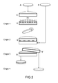
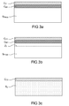
- the substrates are then prepared, for example by chemical mechanical polishing, to be compatible with the subsequent step of direct bonding. This preparation can make it possible to obtain the flatness and the desired roughness for the subsequent direct bonding.
- particles of mastered sizes are deposited / created on one of the two bonding interfaces.
- These particles or ⁇ -pads may, for example, be created by lithography followed by etching or by the deposition of particles of controlled size and in a localized manner.
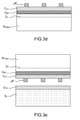
- the figure 3d illustrates a configuration in which ⁇ -plots ⁇ P are made on the surface of the layer C C1 .
- These particles are initiating areas of non-sticking: they prevent the bonding of the two locally substrates at these areas and / or around these areas. Other types of non-bonding initiation zones will be described later.
- the figure 3e illustrates the contacting of the two stacks before the gluing phase.
- the two substrates are then glued by direct bonding as illustrated in the article: Tong & Gösele 1999, Q.-Y. Tong, U. Gösele, Wafer Bonding Semiconductor: Science and Technology, Wiley, New York, 1999, 297 pp .
- This article describes in particular the behavior of a particle at the bonding interface: depending on the size of the particle (especially its height), a blister of a specific radius and of equal height to that of the particle is formed.
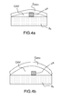
- the Applicant has observed that the height of the gas bubbles is significantly greater than the height of the particles: the diameter and height of the blisters are controlled by the thermal budget applied.
- This thermal budget can also allow two or more contiguous blisters to join together to form a large blister.
- the maximum blister attained is of the order of 1000 ⁇ m in diameter.
- Finishing processes (such as heat treatment and / or polishing to obtain a roughness compatible with the production of components a posteriori) can be performed.
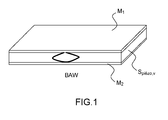
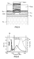
- the final FBAR resonator is produced by depositing an upper metal electrode C M2 at the CAV-formed blister, as illustrated in FIG. figure 5 , furthermore highlighting a zone Z BAW of propagation of acoustic waves of volume.
- the curves of the figure 6 illustrate the electrical response of the suspended membrane obtained according to the method of the invention.
- the curve 6a corresponds to the response of the undissolved piezoelectric layer of the substrate, the curve 6b being relative to said detached diaphragm and thus to the final structure of the FBAR resonator.
- non-bonding initiating zones can be made on the surface of one or both substrates to be assembled to locally prevent the direct bonding of these two substrates and thus to generate at the interface an acoustically decoupling blister. locally these two substrates. It may be in particular hydrocarbon species present on the surface or liquid or solid species. These species can generate gaseous by-products. With a suitable heat treatment, this zone is called to increase in size by the effect of pressure in the unglued zone, so as to generate a suspended membrane zone (side-held). For dimensioning effects we can refer to the articles of Tong and Goesele (book 1999 p.42).
- the bonding energy can be increased during this heat treatment and yet it is not sufficient to prevent the opening of the zone from which the increase of the lateral dimensions r of the unbonded area and its height h.
Landscapes
- Engineering & Computer Science (AREA)
- Manufacturing & Machinery (AREA)
- Physics & Mathematics (AREA)
- Acoustics & Sound (AREA)
- Piezo-Electric Or Mechanical Vibrators, Or Delay Or Filter Circuits (AREA)
- Micromachines (AREA)
- Surface Acoustic Wave Elements And Circuit Networks Thereof (AREA)
Applications Claiming Priority (1)
| Application Number | Priority Date | Filing Date | Title |
|---|---|---|---|
| FR1060358A FR2968861B1 (fr) | 2010-12-10 | 2010-12-10 | Procédé de fabrication d'un résonateur a ondes acoustiques comprenant une membrane suspendue |
Publications (2)
| Publication Number | Publication Date |
|---|---|
| EP2464006A1 true EP2464006A1 (de) | 2012-06-13 |
| EP2464006B1 EP2464006B1 (de) | 2018-05-30 |
Family
ID=45044460
Family Applications (1)
| Application Number | Title | Priority Date | Filing Date |
|---|---|---|---|
| EP11191911.4A Active EP2464006B1 (de) | 2010-12-10 | 2011-12-05 | Herstellungsverfahren eines Schallwellenresonators, der eine aufgehängte Membran umfasst |
Country Status (8)
| Country | Link |
|---|---|
| US (1) | US8715517B2 (de) |
| EP (1) | EP2464006B1 (de) |
| JP (1) | JP6047789B2 (de) |
| KR (1) | KR101910195B1 (de) |
| CN (1) | CN102545814B (de) |
| FR (1) | FR2968861B1 (de) |
| SG (1) | SG184621A1 (de) |
| TW (1) | TWI562412B (de) |
Cited By (1)
| Publication number | Priority date | Publication date | Assignee | Title |
|---|---|---|---|---|
| EP3706180A1 (de) * | 2019-03-05 | 2020-09-09 | Commissariat à l'Energie Atomique et aux Energies Alternatives | Verfahren zur herstellung eines mikroelektromechanischen systems, das aus einer abgeschiedenen piezoelektrischen oder ferroelektrischen schicht hergestellt wird |
Families Citing this family (17)
| Publication number | Priority date | Publication date | Assignee | Title |
|---|---|---|---|---|
| FR2951336B1 (fr) | 2009-10-09 | 2017-02-10 | Commissariat Energie Atomique | Dispositif a ondes acoustiques comprenant un filtre a ondes de surface et un filtre a ondes de volume et procede de fabrication |
| FR2974691B1 (fr) | 2011-04-28 | 2019-08-30 | Commissariat A L'energie Atomique Et Aux Energies Alternatives | Dispositif electromecanique a ondes acoustiques comprenant une zone de transduction et une cavite etendue |
| FR2976126B1 (fr) | 2011-06-01 | 2014-05-09 | Commissariat Energie Atomique | Composant electrique comprenant un materiau de structure perovskite et des electrodes optimisees et procede de fabrication |
| DE102013019434A1 (de) * | 2013-11-20 | 2015-05-21 | Berliner Glas Kgaa Herbert Kubatz Gmbh & Co. | Festkörperfügen eines Trägerkörpers und einer Deckschicht, insbesondere durch anodisches Bonden |
| KR102207928B1 (ko) | 2014-08-13 | 2021-01-26 | 삼성전자주식회사 | 음향 센싱 소자 및 주파수 정보 획득 방법 |
| JP6396854B2 (ja) * | 2015-06-02 | 2018-09-26 | 信越化学工業株式会社 | 酸化物単結晶薄膜を備えた複合ウェーハの製造方法 |
| TWI625446B (zh) * | 2015-06-18 | 2018-06-01 | 德克薩斯大學體系董事會 | 用於抑制來自液體中的源的聲能的共振器、共振器陣列和雜訊消減系統 |
| WO2018182657A1 (en) * | 2017-03-30 | 2018-10-04 | Intel Corporation | Compensation for temperature coefficient of resonant frequency using atomic layer deposition materials |
| CN108365083B (zh) * | 2018-02-07 | 2022-03-08 | 济南晶正电子科技有限公司 | 用于声表面波器件的复合压电衬底的制造方法 |
| US11251769B2 (en) * | 2018-10-18 | 2022-02-15 | Skyworks Solutions, Inc. | Bulk acoustic wave components |
| CN109981069B (zh) * | 2019-03-13 | 2022-03-15 | 电子科技大学 | 具有隔离层的薄膜体声波谐振器制备方法及体声波谐振器 |
| FR3100081B1 (fr) | 2019-08-21 | 2021-09-10 | Commissariat Energie Atomique | Procédé de scellement de cavités par des membranes |
| EP3869575A1 (de) * | 2020-02-21 | 2021-08-25 | Nederlandse Organisatie voor toegepast- natuurwetenschappelijk Onderzoek TNO | Piezoelektrische vorrichtung mit säulenstruktur und herstellungsverfahren |
| FR3108898B1 (fr) * | 2020-04-03 | 2022-08-05 | Univ Paris Saclay | Procede pour generer un ecoulement dans une microgoutte et dispositif pour la mise en œuvre du procede |
| CN111884616B (zh) * | 2020-07-23 | 2021-04-13 | 中国科学院上海微系统与信息技术研究所 | 一种衬底基板/压电材料薄膜结构及其制备方法和应用 |
| FR3132788B1 (fr) * | 2022-02-14 | 2024-01-05 | Soitec Silicon On Insulator | Procede de transfert d’une couche mince sur un substrat support |
| FR3152083B1 (fr) * | 2023-08-07 | 2025-07-11 | Soitec Silicon On Insulator | Procede de transfert d’une couche mince sur un substrat support |
Citations (4)
| Publication number | Priority date | Publication date | Assignee | Title |
|---|---|---|---|---|
| EP0741910A1 (de) | 1994-01-26 | 1996-11-13 | Commissariat A L'energie Atomique | Struktur mit kavitäten und herstellungsverfahren für solch eine struktur |
| EP0851465A1 (de) | 1996-12-09 | 1998-07-01 | Commissariat A L'energie Atomique | Verfahren zum Trennen von mindestens zwei Elementen einer Struktur, die durch Ionenimplantation verbunden sind |
| US20030199105A1 (en) * | 2002-04-22 | 2003-10-23 | Kub Francis J. | Method for making piezoelectric resonator and surface acoustic wave device using hydrogen implant layer splitting |
| US20050255234A1 (en) * | 2004-04-23 | 2005-11-17 | Atsuhiko Kanda | Method for manufacturing resonator |
Family Cites Families (23)
| Publication number | Priority date | Publication date | Assignee | Title |
|---|---|---|---|---|
| JPS506158B1 (de) * | 1970-07-08 | 1975-03-11 | ||
| JPS5226664B2 (de) * | 1972-02-10 | 1977-07-15 | ||
| US5234562A (en) * | 1988-11-07 | 1993-08-10 | Matsushita Electric Industrial Co., Ltd. | Electroplating apparatus for coating a dielectric resonator |
| KR20030039446A (ko) * | 2001-11-13 | 2003-05-22 | 삼성전자주식회사 | Fbar 제조방법 |
| US7830074B2 (en) * | 2006-08-08 | 2010-11-09 | Hrl Laboratories, Llc | Integrated quartz oscillator on an active electronic substrate |
| JP4149416B2 (ja) * | 2004-05-31 | 2008-09-10 | 富士通メディアデバイス株式会社 | 圧電薄膜共振子およびフィルタならびにそれらの製造方法 |
| JP4820609B2 (ja) * | 2004-09-10 | 2011-11-24 | パナソニック株式会社 | 圧電共振器を用いたフィルタモジュール、共用器及び通信機器並びにその製造方法 |
| JP2006101005A (ja) * | 2004-09-28 | 2006-04-13 | Toshiba Corp | 薄膜圧電共振器、高周波回路実装体及び薄膜圧電共振器の製造方法 |
| JP4707503B2 (ja) * | 2005-08-25 | 2011-06-22 | パナソニック株式会社 | 薄膜バルク音響共振器 |
| JP2007213825A (ja) * | 2006-02-07 | 2007-08-23 | Matsushita Electric Ind Co Ltd | 非水電解質二次電池と、その負極活物質および負極、ならびにそれらの製造方法 |
| JP2007221588A (ja) * | 2006-02-17 | 2007-08-30 | Toshiba Corp | 薄膜圧電共振器及び薄膜圧電共振器の製造方法 |
| TW200818691A (en) * | 2006-08-08 | 2008-04-16 | Hrl Lab Llc | An integrated quartz oscillator on an active electronic substrate |
| JP2008252159A (ja) * | 2007-03-29 | 2008-10-16 | Ngk Insulators Ltd | ラダー型圧電フィルタ |
| FR2921192B1 (fr) | 2007-09-17 | 2010-08-20 | Commissariat Energie Atomique | Lentille a immersion solide et procede de realisation associe |
| JP2009124640A (ja) * | 2007-11-19 | 2009-06-04 | Hitachi Media Electoronics Co Ltd | 薄膜圧電バルク波共振器およびその製造方法、並びに薄膜圧電バルク波共振器を用いた薄膜圧電バルク波共振器フィルタ |
| JP5168568B2 (ja) * | 2008-09-01 | 2013-03-21 | Tdk株式会社 | 薄膜バルク波共振器 |
| JP4743258B2 (ja) * | 2008-10-31 | 2011-08-10 | 株式会社村田製作所 | 圧電デバイスの製造方法 |
| US8507860B2 (en) * | 2009-05-20 | 2013-08-13 | Nutech Ventures | Terahertz resonator |
| FR2950197A1 (fr) | 2009-09-15 | 2011-03-18 | Commissariat Energie Atomique | Membrane piezoelectrique a actionnement optimise et procede de fabrication de la membrane |
| FR2951014B1 (fr) | 2009-10-06 | 2011-11-25 | Commissariat Energie Atomique | Structure d'actionnement piezoelectrique comportant une jauge de contrainte piezoresistive integree et son procede de realisation |
| FR2953647B1 (fr) | 2009-12-04 | 2011-11-25 | Commissariat Energie Atomique | Procede de realisation d'un resonateur acoustique a ondes de volumes de type fbar |
| FR2962613B1 (fr) | 2010-07-06 | 2013-08-16 | Commissariat Energie Atomique | Dispositif d'adaptation d'impedance d'un composant comportant un filtre a impedance adaptable a base de materiau de type perovskite |
| FR2964497B1 (fr) | 2010-09-03 | 2013-04-19 | Commissariat Energie Atomique | Capacité intégrée comprenant une couche d'isolation électrique en matériau de type perovskite amorphe et procédé de fabrication |
-
2010
- 2010-12-10 FR FR1060358A patent/FR2968861B1/fr not_active Expired - Fee Related
-
2011
- 2011-12-05 EP EP11191911.4A patent/EP2464006B1/de active Active
- 2011-12-06 SG SG2011090834A patent/SG184621A1/en unknown
- 2011-12-08 US US13/314,844 patent/US8715517B2/en active Active
- 2011-12-09 TW TW100145537A patent/TWI562412B/zh active
- 2011-12-09 CN CN201110462242.9A patent/CN102545814B/zh active Active
- 2011-12-09 KR KR1020110132303A patent/KR101910195B1/ko active Active
- 2011-12-09 JP JP2011270459A patent/JP6047789B2/ja active Active
Patent Citations (4)
| Publication number | Priority date | Publication date | Assignee | Title |
|---|---|---|---|---|
| EP0741910A1 (de) | 1994-01-26 | 1996-11-13 | Commissariat A L'energie Atomique | Struktur mit kavitäten und herstellungsverfahren für solch eine struktur |
| EP0851465A1 (de) | 1996-12-09 | 1998-07-01 | Commissariat A L'energie Atomique | Verfahren zum Trennen von mindestens zwei Elementen einer Struktur, die durch Ionenimplantation verbunden sind |
| US20030199105A1 (en) * | 2002-04-22 | 2003-10-23 | Kub Francis J. | Method for making piezoelectric resonator and surface acoustic wave device using hydrogen implant layer splitting |
| US20050255234A1 (en) * | 2004-04-23 | 2005-11-17 | Atsuhiko Kanda | Method for manufacturing resonator |
Non-Patent Citations (13)
| Title |
|---|
| F. RIEUTORD, ECS, 2010 |
| H. CAMPANELLA; J. ESTEVE; E. MARTINCIC; P. NOUET; A. URANGA; N. BARNIOL, IEEE SENSORS, 2008 |
| J. KAITILA: "Review of wave propagation in BAW thin film devices: progress and prospects", PROCEEDINGS OF THE 2007 IEEE ULTRASONICS SYMPOSIUM, 2007 |
| M. BRUEL: "Silicon on insulator material technology", ELECTRONIC LETTERS, vol. 31, no. 14, 1995, pages 1201 - 1202, XP006003062, DOI: doi:10.1049/el:19950805 |
| M. PIJOLAT; S. LOUBRIAT; S. QUESTE; D. MERCIER; A. REINHARDT; E. DEFAŸ; C. DEGUET; L. CLAVELIER; H. MORICEAU; M. AÏD, APPL. PHYS. LETT, vol. 95, 2009, pages 182106 |
| P. MURALT ET AL.: "Ils there a better material for thin film BAW applications than AIN", PROCEEDINGS OF THE 2005 IEEE ULTRASONICS SYMPOSIUM |
| P. MURALT ET AL.: "Is there a better material for thin film BAW applications than AIN", PROCEEDINGS OF THE 2005 IEEE ULTRASONICS SYMPOSIUM., 2005 |
| PIJOLAT M ET AL: "Large electromechanical coupling factor film bulk acoustic resonator with X-cut LiNbO3 layer transfer", APPLIED PHYSICS LETTERS, AIP, vol. 95, no. 18, 5 November 2009 (2009-11-05), pages 182106 - 182106, XP012126324 * |
| R. AIGNER: "Bringing BAW technology into volume production : the Ten Commandments and the seven deadly sins", PROCEEDINGS OF THE THIRD INTERNATIONAL SYMPOSIUM ON ACOUSTIC WAVE DEVICES FOR FUTURE MOBILE COMMUNICATION SYSTEMS, 2007 |
| R. AIGNER: "Bringing BAW technology into volume production: the Ten Commandments and the seven deadly sins", PROCEEDINGS OF THE THIRD INTERNATIONAL SYMPOSIUM ON ACOUSTIC WAVE DEVICES FOR FUTURE MOBILE COMMUNICATION SYSTEMS, 2007 |
| TONG Q-Y ET AL: "Semiconductor wafer bonding: recent developments", MATERIALS CHEMISTRY AND PHYSICS, ELSEVIER, vol. 37, no. 2, 1 March 1994 (1994-03-01), pages 101 - 127, XP024148341 * |
| TONG; GÔSELE; Q.-Y. TONG; U. GÔSELE: "Semiconductor Wafer Bonding: Science and Technology", 1999, WILEY, pages: 297 |
| W. STEICHEN; S. BALLANDRAS: "Composants acoustiques utilisés pour le filtrage : revues de différentes technologies", EDITIONS DE TECHNIQUES DE L'INGÉNIEUR, 2008, pages E-2000,31 |
Cited By (4)
| Publication number | Priority date | Publication date | Assignee | Title |
|---|---|---|---|---|
| EP3706180A1 (de) * | 2019-03-05 | 2020-09-09 | Commissariat à l'Energie Atomique et aux Energies Alternatives | Verfahren zur herstellung eines mikroelektromechanischen systems, das aus einer abgeschiedenen piezoelektrischen oder ferroelektrischen schicht hergestellt wird |
| FR3093511A1 (fr) * | 2019-03-05 | 2020-09-11 | Commissariat A L'energie Atomique Et Aux Energies Alternatives | Procédé de réalisation d’un système micro-électro-mécanique réalisé à partir d’une couche piézoélectrique ou ferroélectrique reportée |
| EP4075528A1 (de) | 2019-03-05 | 2022-10-19 | Commissariat à l'énergie atomique et aux énergies alternatives | Verfahren zur herstellung eines mikro-elektro-mechanischen systems aus einer übertragenen piezoelektrischen oder ferroelektrischen schicht |
| US11705880B2 (en) | 2019-03-05 | 2023-07-18 | Commissariat A L'energie Atomique Et Aux Energies Alternatives | Process for producing a micro-electro-mechanical system from a transferred piezoelectric or ferroelectric layer |
Also Published As
| Publication number | Publication date |
|---|---|
| TWI562412B (en) | 2016-12-11 |
| EP2464006B1 (de) | 2018-05-30 |
| FR2968861A1 (fr) | 2012-06-15 |
| US20120145667A1 (en) | 2012-06-14 |
| CN102545814B (zh) | 2017-03-01 |
| US8715517B2 (en) | 2014-05-06 |
| FR2968861B1 (fr) | 2013-09-27 |
| KR101910195B1 (ko) | 2018-10-19 |
| SG184621A1 (en) | 2012-10-30 |
| JP2012147423A (ja) | 2012-08-02 |
| KR20120065262A (ko) | 2012-06-20 |
| CN102545814A (zh) | 2012-07-04 |
| TW201244197A (en) | 2012-11-01 |
| JP6047789B2 (ja) | 2016-12-21 |
Similar Documents
| Publication | Publication Date | Title |
|---|---|---|
| EP2464006B1 (de) | Herstellungsverfahren eines Schallwellenresonators, der eine aufgehängte Membran umfasst | |
| EP2486655B1 (de) | Schallwellenvorrichtug mit einem oberflächenwellenfilter und einem volumenwellenfilter sowie herstellungsverfahren dafür | |
| EP2628243B1 (de) | Heterogene akustische struktur aus einem homogenen material | |
| EP3859800B1 (de) | Hybridstruktur für vorrichtung mit oberflächenschallwellen | |
| EP4075528B1 (de) | Verfahren zur herstellung eines mikro-elektro-mechanischen systems aus einer aufgetragenen piezoelektrischen oder ferroelektrischen schicht | |
| EP4006998B1 (de) | Verfahren zur herstellung eines bauteils mit einer schicht aus monokristallinem material, das mit hohen wärmehaushalten kompatibel ist | |
| FR3045677B1 (fr) | Procede de fabrication d'une couche monocristalline, notamment piezoelectrique | |
| EP2642662B1 (de) | HBAR-Resonator, der eine Amplitudenverstärkungsstruktur von mindestens einer Resonanz des entsprechenden Resonators umfasst, und Verfahren zur Herstellung dieses Resonators | |
| EP2764616A1 (de) | Elektroakustischer wandler mit periodischer ferroelektrischer polarisation auf einer mikrogefertigten vertikalern struktur | |
| EP3394323A1 (de) | Verfahren zur herstellung einer monokristallinen piezoelektrischen schicht und mikroelektronische, fotonische oder optische vorrichtung mit solch einer schicht | |
| FR2889887A1 (fr) | Procede de report d'une couche mince sur un support | |
| WO2011076806A1 (fr) | Dispositif electromecanique a base d'electret mineral, et son procede de fabrication | |
| EP3365929B1 (de) | Verfahren zur herstellung einer hybridstruktur | |
| EP3465788B1 (de) | Verfahren zur herstellung einer schicht | |
| WO2019121886A1 (fr) | Procédé de fabrication de composite à couche mince ultra-plane |
Legal Events
| Date | Code | Title | Description |
|---|---|---|---|
| PUAI | Public reference made under article 153(3) epc to a published international application that has entered the european phase |
Free format text: ORIGINAL CODE: 0009012 |
|
| AK | Designated contracting states |
Kind code of ref document: A1 Designated state(s): AL AT BE BG CH CY CZ DE DK EE ES FI FR GB GR HR HU IE IS IT LI LT LU LV MC MK MT NL NO PL PT RO RS SE SI SK SM TR |
|
| AX | Request for extension of the european patent |
Extension state: BA ME |
|
| 17P | Request for examination filed |
Effective date: 20121207 |
|
| 17Q | First examination report despatched |
Effective date: 20140904 |
|
| GRAP | Despatch of communication of intention to grant a patent |
Free format text: ORIGINAL CODE: EPIDOSNIGR1 |
|
| STAA | Information on the status of an ep patent application or granted ep patent |
Free format text: STATUS: GRANT OF PATENT IS INTENDED |
|
| INTG | Intention to grant announced |
Effective date: 20180208 |
|
| GRAS | Grant fee paid |
Free format text: ORIGINAL CODE: EPIDOSNIGR3 |
|
| GRAA | (expected) grant |
Free format text: ORIGINAL CODE: 0009210 |
|
| STAA | Information on the status of an ep patent application or granted ep patent |
Free format text: STATUS: THE PATENT HAS BEEN GRANTED |
|
| AK | Designated contracting states |
Kind code of ref document: B1 Designated state(s): AL AT BE BG CH CY CZ DE DK EE ES FI FR GB GR HR HU IE IS IT LI LT LU LV MC MK MT NL NO PL PT RO RS SE SI SK SM TR |
|
| REG | Reference to a national code |
Ref country code: GB Ref legal event code: FG4D Free format text: NOT ENGLISH |
|
| REG | Reference to a national code |
Ref country code: CH Ref legal event code: EP |
|
| REG | Reference to a national code |
Ref country code: AT Ref legal event code: REF Ref document number: 1004643 Country of ref document: AT Kind code of ref document: T Effective date: 20180615 |
|
| REG | Reference to a national code |
Ref country code: IE Ref legal event code: FG4D Free format text: LANGUAGE OF EP DOCUMENT: FRENCH |
|
| REG | Reference to a national code |
Ref country code: DE Ref legal event code: R096 Ref document number: 602011048739 Country of ref document: DE |
|
| REG | Reference to a national code |
Ref country code: NL Ref legal event code: MP Effective date: 20180530 |
|
| REG | Reference to a national code |
Ref country code: LT Ref legal event code: MG4D |
|
| PG25 | Lapsed in a contracting state [announced via postgrant information from national office to epo] |
Ref country code: ES Free format text: LAPSE BECAUSE OF FAILURE TO SUBMIT A TRANSLATION OF THE DESCRIPTION OR TO PAY THE FEE WITHIN THE PRESCRIBED TIME-LIMIT Effective date: 20180530 Ref country code: BG Free format text: LAPSE BECAUSE OF FAILURE TO SUBMIT A TRANSLATION OF THE DESCRIPTION OR TO PAY THE FEE WITHIN THE PRESCRIBED TIME-LIMIT Effective date: 20180830 Ref country code: LT Free format text: LAPSE BECAUSE OF FAILURE TO SUBMIT A TRANSLATION OF THE DESCRIPTION OR TO PAY THE FEE WITHIN THE PRESCRIBED TIME-LIMIT Effective date: 20180530 Ref country code: CY Free format text: LAPSE BECAUSE OF FAILURE TO SUBMIT A TRANSLATION OF THE DESCRIPTION OR TO PAY THE FEE WITHIN THE PRESCRIBED TIME-LIMIT Effective date: 20180530 Ref country code: FI Free format text: LAPSE BECAUSE OF FAILURE TO SUBMIT A TRANSLATION OF THE DESCRIPTION OR TO PAY THE FEE WITHIN THE PRESCRIBED TIME-LIMIT Effective date: 20180530 Ref country code: NO Free format text: LAPSE BECAUSE OF FAILURE TO SUBMIT A TRANSLATION OF THE DESCRIPTION OR TO PAY THE FEE WITHIN THE PRESCRIBED TIME-LIMIT Effective date: 20180830 Ref country code: SE Free format text: LAPSE BECAUSE OF FAILURE TO SUBMIT A TRANSLATION OF THE DESCRIPTION OR TO PAY THE FEE WITHIN THE PRESCRIBED TIME-LIMIT Effective date: 20180530 |
|
| PG25 | Lapsed in a contracting state [announced via postgrant information from national office to epo] |
Ref country code: RS Free format text: LAPSE BECAUSE OF FAILURE TO SUBMIT A TRANSLATION OF THE DESCRIPTION OR TO PAY THE FEE WITHIN THE PRESCRIBED TIME-LIMIT Effective date: 20180530 Ref country code: LV Free format text: LAPSE BECAUSE OF FAILURE TO SUBMIT A TRANSLATION OF THE DESCRIPTION OR TO PAY THE FEE WITHIN THE PRESCRIBED TIME-LIMIT Effective date: 20180530 Ref country code: HR Free format text: LAPSE BECAUSE OF FAILURE TO SUBMIT A TRANSLATION OF THE DESCRIPTION OR TO PAY THE FEE WITHIN THE PRESCRIBED TIME-LIMIT Effective date: 20180530 Ref country code: GR Free format text: LAPSE BECAUSE OF FAILURE TO SUBMIT A TRANSLATION OF THE DESCRIPTION OR TO PAY THE FEE WITHIN THE PRESCRIBED TIME-LIMIT Effective date: 20180831 |
|
| REG | Reference to a national code |
Ref country code: AT Ref legal event code: MK05 Ref document number: 1004643 Country of ref document: AT Kind code of ref document: T Effective date: 20180530 |
|
| PG25 | Lapsed in a contracting state [announced via postgrant information from national office to epo] |
Ref country code: NL Free format text: LAPSE BECAUSE OF FAILURE TO SUBMIT A TRANSLATION OF THE DESCRIPTION OR TO PAY THE FEE WITHIN THE PRESCRIBED TIME-LIMIT Effective date: 20180530 |
|
| PG25 | Lapsed in a contracting state [announced via postgrant information from national office to epo] |
Ref country code: SK Free format text: LAPSE BECAUSE OF FAILURE TO SUBMIT A TRANSLATION OF THE DESCRIPTION OR TO PAY THE FEE WITHIN THE PRESCRIBED TIME-LIMIT Effective date: 20180530 Ref country code: RO Free format text: LAPSE BECAUSE OF FAILURE TO SUBMIT A TRANSLATION OF THE DESCRIPTION OR TO PAY THE FEE WITHIN THE PRESCRIBED TIME-LIMIT Effective date: 20180530 Ref country code: PL Free format text: LAPSE BECAUSE OF FAILURE TO SUBMIT A TRANSLATION OF THE DESCRIPTION OR TO PAY THE FEE WITHIN THE PRESCRIBED TIME-LIMIT Effective date: 20180530 Ref country code: CZ Free format text: LAPSE BECAUSE OF FAILURE TO SUBMIT A TRANSLATION OF THE DESCRIPTION OR TO PAY THE FEE WITHIN THE PRESCRIBED TIME-LIMIT Effective date: 20180530 Ref country code: AT Free format text: LAPSE BECAUSE OF FAILURE TO SUBMIT A TRANSLATION OF THE DESCRIPTION OR TO PAY THE FEE WITHIN THE PRESCRIBED TIME-LIMIT Effective date: 20180530 Ref country code: EE Free format text: LAPSE BECAUSE OF FAILURE TO SUBMIT A TRANSLATION OF THE DESCRIPTION OR TO PAY THE FEE WITHIN THE PRESCRIBED TIME-LIMIT Effective date: 20180530 Ref country code: DK Free format text: LAPSE BECAUSE OF FAILURE TO SUBMIT A TRANSLATION OF THE DESCRIPTION OR TO PAY THE FEE WITHIN THE PRESCRIBED TIME-LIMIT Effective date: 20180530 |
|
| PG25 | Lapsed in a contracting state [announced via postgrant information from national office to epo] |
Ref country code: SM Free format text: LAPSE BECAUSE OF FAILURE TO SUBMIT A TRANSLATION OF THE DESCRIPTION OR TO PAY THE FEE WITHIN THE PRESCRIBED TIME-LIMIT Effective date: 20180530 |
|
| REG | Reference to a national code |
Ref country code: DE Ref legal event code: R097 Ref document number: 602011048739 Country of ref document: DE |
|
| PLBE | No opposition filed within time limit |
Free format text: ORIGINAL CODE: 0009261 |
|
| STAA | Information on the status of an ep patent application or granted ep patent |
Free format text: STATUS: NO OPPOSITION FILED WITHIN TIME LIMIT |
|
| 26N | No opposition filed |
Effective date: 20190301 |
|
| PG25 | Lapsed in a contracting state [announced via postgrant information from national office to epo] |
Ref country code: SI Free format text: LAPSE BECAUSE OF FAILURE TO SUBMIT A TRANSLATION OF THE DESCRIPTION OR TO PAY THE FEE WITHIN THE PRESCRIBED TIME-LIMIT Effective date: 20180530 |
|
| REG | Reference to a national code |
Ref country code: CH Ref legal event code: PL |
|
| PG25 | Lapsed in a contracting state [announced via postgrant information from national office to epo] |
Ref country code: LU Free format text: LAPSE BECAUSE OF NON-PAYMENT OF DUE FEES Effective date: 20181205 Ref country code: MC Free format text: LAPSE BECAUSE OF FAILURE TO SUBMIT A TRANSLATION OF THE DESCRIPTION OR TO PAY THE FEE WITHIN THE PRESCRIBED TIME-LIMIT Effective date: 20180530 |
|
| REG | Reference to a national code |
Ref country code: IE Ref legal event code: MM4A |
|
| REG | Reference to a national code |
Ref country code: BE Ref legal event code: MM Effective date: 20181231 |
|
| PG25 | Lapsed in a contracting state [announced via postgrant information from national office to epo] |
Ref country code: IE Free format text: LAPSE BECAUSE OF NON-PAYMENT OF DUE FEES Effective date: 20181205 |
|
| PG25 | Lapsed in a contracting state [announced via postgrant information from national office to epo] |
Ref country code: BE Free format text: LAPSE BECAUSE OF NON-PAYMENT OF DUE FEES Effective date: 20181231 Ref country code: AL Free format text: LAPSE BECAUSE OF FAILURE TO SUBMIT A TRANSLATION OF THE DESCRIPTION OR TO PAY THE FEE WITHIN THE PRESCRIBED TIME-LIMIT Effective date: 20180530 |
|
| PG25 | Lapsed in a contracting state [announced via postgrant information from national office to epo] |
Ref country code: CH Free format text: LAPSE BECAUSE OF NON-PAYMENT OF DUE FEES Effective date: 20181231 Ref country code: LI Free format text: LAPSE BECAUSE OF NON-PAYMENT OF DUE FEES Effective date: 20181231 |
|
| PG25 | Lapsed in a contracting state [announced via postgrant information from national office to epo] |
Ref country code: MT Free format text: LAPSE BECAUSE OF FAILURE TO SUBMIT A TRANSLATION OF THE DESCRIPTION OR TO PAY THE FEE WITHIN THE PRESCRIBED TIME-LIMIT Effective date: 20180530 |
|
| PG25 | Lapsed in a contracting state [announced via postgrant information from national office to epo] |
Ref country code: TR Free format text: LAPSE BECAUSE OF FAILURE TO SUBMIT A TRANSLATION OF THE DESCRIPTION OR TO PAY THE FEE WITHIN THE PRESCRIBED TIME-LIMIT Effective date: 20180530 |
|
| PG25 | Lapsed in a contracting state [announced via postgrant information from national office to epo] |
Ref country code: PT Free format text: LAPSE BECAUSE OF FAILURE TO SUBMIT A TRANSLATION OF THE DESCRIPTION OR TO PAY THE FEE WITHIN THE PRESCRIBED TIME-LIMIT Effective date: 20180530 |
|
| PG25 | Lapsed in a contracting state [announced via postgrant information from national office to epo] |
Ref country code: HU Free format text: LAPSE BECAUSE OF FAILURE TO SUBMIT A TRANSLATION OF THE DESCRIPTION OR TO PAY THE FEE WITHIN THE PRESCRIBED TIME-LIMIT; INVALID AB INITIO Effective date: 20111205 Ref country code: MK Free format text: LAPSE BECAUSE OF NON-PAYMENT OF DUE FEES Effective date: 20180530 |
|
| PG25 | Lapsed in a contracting state [announced via postgrant information from national office to epo] |
Ref country code: IS Free format text: LAPSE BECAUSE OF FAILURE TO SUBMIT A TRANSLATION OF THE DESCRIPTION OR TO PAY THE FEE WITHIN THE PRESCRIBED TIME-LIMIT Effective date: 20180930 |
|
| PGFP | Annual fee paid to national office [announced via postgrant information from national office to epo] |
Ref country code: GB Payment date: 20251229 Year of fee payment: 15 |
|
| PGFP | Annual fee paid to national office [announced via postgrant information from national office to epo] |
Ref country code: FR Payment date: 20251222 Year of fee payment: 15 |
|
| PGFP | Annual fee paid to national office [announced via postgrant information from national office to epo] |
Ref country code: DE Payment date: 20251222 Year of fee payment: 15 |
|
| PGFP | Annual fee paid to national office [announced via postgrant information from national office to epo] |
Ref country code: IT Payment date: 20251231 Year of fee payment: 15 |