EP2464023B1 - Dispositif de communication avec plusieurs voies de réception et de transmission et procédés associés - Google Patents
Dispositif de communication avec plusieurs voies de réception et de transmission et procédés associés Download PDFInfo
- Publication number
- EP2464023B1 EP2464023B1 EP11193116.8A EP11193116A EP2464023B1 EP 2464023 B1 EP2464023 B1 EP 2464023B1 EP 11193116 A EP11193116 A EP 11193116A EP 2464023 B1 EP2464023 B1 EP 2464023B1
- Authority
- EP
- European Patent Office
- Prior art keywords
- bandwidth
- frequency band
- pass filter
- band
- receive path
- Prior art date
- Legal status (The legal status is an assumption and is not a legal conclusion. Google has not performed a legal analysis and makes no representation as to the accuracy of the status listed.)
- Active
Links
Images


Classifications
-
- H—ELECTRICITY
- H04—ELECTRIC COMMUNICATION TECHNIQUE
- H04B—TRANSMISSION
- H04B1/00—Details of transmission systems, not covered by a single one of groups H04B3/00 - H04B13/00; Details of transmission systems not characterised by the medium used for transmission
- H04B1/38—Transceivers, i.e. devices in which transmitter and receiver form a structural unit and in which at least one part is used for functions of transmitting and receiving
- H04B1/40—Circuits
- H04B1/403—Circuits using the same oscillator for generating both the transmitter frequency and the receiver local oscillator frequency
- H04B1/406—Circuits using the same oscillator for generating both the transmitter frequency and the receiver local oscillator frequency with more than one transmission mode, e.g. analog and digital modes
-
- H—ELECTRICITY
- H04—ELECTRIC COMMUNICATION TECHNIQUE
- H04B—TRANSMISSION
- H04B1/00—Details of transmission systems, not covered by a single one of groups H04B3/00 - H04B13/00; Details of transmission systems not characterised by the medium used for transmission
- H04B1/005—Details of transmission systems, not covered by a single one of groups H04B3/00 - H04B13/00; Details of transmission systems not characterised by the medium used for transmission adapting radio receivers, transmitters andtransceivers for operation on two or more bands, i.e. frequency ranges
- H04B1/0053—Details of transmission systems, not covered by a single one of groups H04B3/00 - H04B13/00; Details of transmission systems not characterised by the medium used for transmission adapting radio receivers, transmitters andtransceivers for operation on two or more bands, i.e. frequency ranges with common antenna for more than one band
-
- H—ELECTRICITY
- H04—ELECTRIC COMMUNICATION TECHNIQUE
- H04B—TRANSMISSION
- H04B1/00—Details of transmission systems, not covered by a single one of groups H04B3/00 - H04B13/00; Details of transmission systems not characterised by the medium used for transmission
- H04B1/005—Details of transmission systems, not covered by a single one of groups H04B3/00 - H04B13/00; Details of transmission systems not characterised by the medium used for transmission adapting radio receivers, transmitters andtransceivers for operation on two or more bands, i.e. frequency ranges
- H04B1/0053—Details of transmission systems, not covered by a single one of groups H04B3/00 - H04B13/00; Details of transmission systems not characterised by the medium used for transmission adapting radio receivers, transmitters andtransceivers for operation on two or more bands, i.e. frequency ranges with common antenna for more than one band
- H04B1/0057—Details of transmission systems, not covered by a single one of groups H04B3/00 - H04B13/00; Details of transmission systems not characterised by the medium used for transmission adapting radio receivers, transmitters andtransceivers for operation on two or more bands, i.e. frequency ranges with common antenna for more than one band using diplexing or multiplexing filters for selecting the desired band
-
- H—ELECTRICITY
- H04—ELECTRIC COMMUNICATION TECHNIQUE
- H04B—TRANSMISSION
- H04B1/00—Details of transmission systems, not covered by a single one of groups H04B3/00 - H04B13/00; Details of transmission systems not characterised by the medium used for transmission
- H04B1/38—Transceivers, i.e. devices in which transmitter and receiver form a structural unit and in which at least one part is used for functions of transmitting and receiving
- H04B1/40—Circuits
- H04B1/50—Circuits using different frequencies for the two directions of communication
- H04B1/52—Hybrid arrangements, i.e. arrangements for transition from single-path two-direction transmission to single-direction transmission on each of two paths or vice versa
- H04B1/525—Hybrid arrangements, i.e. arrangements for transition from single-path two-direction transmission to single-direction transmission on each of two paths or vice versa with means for reducing leakage of transmitter signal into the receiver
Definitions
- This application relates to the field of communications, and more particularly, to wireless communications systems and related methods.
- PDA Personal Digital Assistant
- US2009/0180403 discloses a multi-band, multi-mode radio frequency front end module capable of operating in widely different frequency bands.
- a communications device may include a first transmit path comprising a first band pass filter operating at a first frequency band having a first bandwidth, and a second transmit path comprising a second band pass filter operating at a second frequency band having a second bandwidth.
- the second frequency band may be adjacent the first frequency band, and the second bandwidth may be less than the first bandwidth.
- the communications device may also include a third receive path operating at a third frequency band having a third bandwidth, and a fourth receive path operating at a fourth frequency band having a fourth bandwidth, the fourth frequency band being adjacent the third frequency band and the fourth bandwidth being less than the third bandwidth.
- the communications device may also include an antenna, and a first duplex band pass filter coupling the first transmit path and the third receive path to the antenna.
- the first duplex band pass filter may be configured to selectively pass the first frequency band for the first transmit path and the third frequency band for the third receive path.
- the communications device may further comprise a switch configured to selectively couple the first and second duplex band pass filters to the antenna.
- the communications device may further comprise a second antenna, and a fifth receive path coupled to the second antenna.
- the fifth receive path may comprise a band pass filter configured to pass a combined bandwidth of the third and fourth frequency bands.
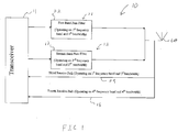
- the communications device 10 illustratively includes a first transmit path 21 , a second transmit path 12 , a third receive path 29 , a fourth receive path 16 , and a transceiver 11 coupled to each of these paths.
- the first transmit path 21 illustratively includes a first band pass filter 22 operating at a first frequency band 51 having a first bandwidth.
- the second transmit path 12 illustratively includes a second band pass filter 13 operating at a second frequency band 52 having a second bandwidth.
- the transceiver 11 is illustratively shown as a QTR8600 chipset, as available from the Qualcomm Corporation of San Diego, CA, but may comprise any capable transceiver chipset. Moreover, the communications device 10 may further comprise a digital signal processor (not shown) upstream of the transceiver 11 .
- the first transmit path 21 further illustratively includes a first power amplifier 23 coupled upstream of the first band pass filter 22 .
- the second transmit path 12 illustratively includes a second power amplifier 14 coupled upstream of the second band pass filter 13 .
- the second frequency band 52 is illustratively adjacent the first frequency band 51 , and the second bandwidth may be less than the first bandwidth.
- the third receive path 29 illustratively operates at a third frequency band 53 having a third bandwidth
- the fourth receive path 16 illustratively operates at a fourth frequency band 54 having a fourth bandwidth
- the fourth frequency band 54 is illustratively adjacent the third frequency band 53 , and the fourth bandwidth is less than the third bandwidth.
- the first and third frequency bands 51 , 53 respectively comprise the 1850-1910 MHz band and the 1930-1990 MHz band
- the second and fourth frequency bands 52 , 54 respectively comprise the 1910-1915 MHz band and the 1990-1995 MHz band.
- the communications device 10 illustratively includes a second duplex band pass filter 15 coupling the second transmit path 12 and the fourth receive path 16 to the switch 61 and the antenna 60 .
- the second duplex band pass filter 15 may be configured to selectively pass the second frequency band 52 for the second transmit path 12 and the fourth frequency band 54 for the fourth receive path 16 .
- the communications device 10 also illustratively includes a sixth transmit path 30 comprising a band pass filter 31 and a power amplifier 32 coupled upstream thereto, a seventh receive path 26 , and a third duplex band pass filter 24 .
- the sixth and seventh paths 30 , 26 illustratively operate at cellular frequencies to provide voice services, and are coupled to the switch 61 via the third duplex band pass filter 24 , which is configured to pass a sixth frequency band for the sixth transmit path 30 and a seventh frequency band for the seventh receive path 26 .
- the switch 61 configured to selectively couple the first, second, and third duplex band pass filters 15 , 24-25 to the antenna 60 depending on the type of communication signals being received and transmitted.
- the communications device also illustratively includes an eighth cellular receive path 36 comprising a band pass filter 35 and for providing diversity to the seventh receive path 26 .
- the communications device 10 also illustratively includes a band pass filter 34 coupling the diversity fifth receive path 37 and the eighth cellular receive path 36 to the second antenna 27 .
- the communications device 10 also illustratively includes a global positioning system (GPS) antenna 28 , and a ninth receive path 40 comprising two band pass filters 41-42 , and a power amplifier 43 coupled thereto for providing GPS receiver input to the transceiver 11 .
- GPS global positioning system
- the breaking up of the PCS transmit and receive paths into four paths 12 , 21 , 16 , 29 may provide for easier design.
- the associated band pass filters 13 , 22 and the duplex band pass filters 15 , 25 are provided with larger guard bands and more roll off space.
- the communications device 10 provides high isolation of the desired frequencies for each transmit/receive path, thereby providing excellent radio frequency (RF) performance.
- the Block G frequency band of the PCS is separated into its own transmit and receive paths, thereby allowing the communications device 10 to use typical filter (e.g. SAW filter) and amplifier components for the typical PCS band paths, thereby reducing the complexity and cost of the communications device.
- typical filter e.g. SAW filter
- amplifier components for the typical PCS band paths
- the housing 1200 may be elongated vertically, or may take on other sizes and shapes (including clamshell housing structures).
- the keypad may include a mode selection key, or other hardware or software for switching between text entry and telephony entry.
- Operating system software executed by the processing device 1800 is stored in a persistent store, such as the flash memory 1160 , but may be stored in other types of memory devices, such as a read only memory (ROM) or similar storage element.
- system software, specific device applications, or parts thereof may be temporarily loaded into a volatile store, such as the random access memory (RAM) 1180 .
- Communications signals received by the mobile device may also be stored in the RAM 1180 .
- the processing device 1800 in addition to its operating system functions, enables execution of software applications 1300A-1300N on the device 1000 .
- a personal information manager (PIM) application may be installed during manufacture.
- the PIM may be capable of organizing and managing data items, such as e-mail, calendar events, voice mails, appointments, and task items.
- the PIM application may also be capable of sending and receiving data items via a wireless network 1401 .
- the PIM data items may be seamlessly integrated, synchronized and updated via the wireless network 1401 with corresponding data items stored or associated with a host computer system.
- the communications subsystem 1001 includes a receiver 1500 , a transmitter 1520 , and one or more antennas 1540 and 1560 .
- the communications subsystem 1001 also includes a processing module, such as a digital signal processor (DSP) 1580 , and local oscillators (LOs) 1601 .
- DSP digital signal processor
- LOs local oscillators
- a mobile device 1000 may include a communications subsystem 1001 designed to operate with the MobitexTM, Data TACTM or General Packet Radio Service (GPRS) mobile data communications networks, and also designed to operate with any of a variety of voice communications networks, such as Advanced Mobile Phone System (AMPS), time division multiple access (TDMA), code division multiple access (CDMA), Wideband code division multiple access (W-CDMA), personal communications service (PCS), GSM (Global System for Mobile Communications), enhanced data rates for GSM evolution (EDGE), etc.
- AMPS Advanced Mobile Phone System
- TDMA time division multiple access
- CDMA code division multiple access
- W-CDMA Wideband code division multiple access
- PCS personal communications service
- GSM Global System for Mobile Communications
- EDGE enhanced data rates for GSM evolution
- Other types of data and voice networks, both separate and integrated, may also be utilized with the mobile device 1000 .
- the mobile device 1000 may also be compliant with other communications standards such as 3GSM, 3rd Generation Partnership Project (3GPP), Universal Mobile Telecommunication
- Network access requirements vary depending upon the type of communication system. For example, in the Mobitex and DataTAC networks, mobile devices are registered on the network using a unique personal identification number or PIN associated with each device. In GPRS networks, however, network access is associated with a subscriber or user of a device. A GPRS device therefore typically involves use of a subscriber identity module, commonly referred to as a SIM card, in order to operate on a GPRS network.
- SIM card subscriber identity module
- the mobile device 1000 may send and receive communications signals over the communication network 1401 .
- Signals received from the communications network 1401 by the antenna 1540 are routed to the receiver 1500 , which provides for signal amplification, frequency down conversion, filtering, channel selection, etc., and may also provide analog to digital conversion. Analog-to-digital conversion of the received signal allows the DSP 1580 to perform more complex communications functions, such as demodulation and decoding.
- signals to be transmitted to the network 1401 are processed (e.g. modulated and encoded) by the DSP 1580 and are then provided to the transmitter 1520 for digital to analog conversion, frequency up conversion, filtering, amplification and transmission to the communication network 1401 (or networks) via the antenna 1560 .
- the DSP 1580 provides for control of the receiver 1500 and the transmitter 1520 .
- gains applied to communications signals in the receiver 1500 and transmitter 1520 may be adaptively controlled through automatic gain control algorithms implemented in the DSP 1580 .
- a received signal such as a text message or web page download
- the communications subsystem 1001 is input to the processing device 1800 .
- the received signal is then further processed by the processing device 1800 for an output to the display 1600 , or alternatively to some other auxiliary I/O device 1060 .
- a device may also be used to compose data items, such as e-mail messages, using the keypad 1400 and/or some other auxiliary I/O device 1060 , such as a touchpad, a rocker switch, a thumb-wheel, or some other type of input device.
- the composed data items may then be transmitted over the communications network 1401 via the communications subsystem 1001 .
- the short-range communications subsystem enables communication between the mobile device 1000 and other proximate systems or devices, which need not necessarily be similar devices.
- the short-range communications subsystem may include an infrared device and associated circuits and components, a BluetoothTM communications module to provide for communication with similarly-enabled systems and devices, or a NFC sensor for communicating with a NFC device or NFC tag via NFC communications.
Landscapes
- Engineering & Computer Science (AREA)
- Computer Networks & Wireless Communication (AREA)
- Signal Processing (AREA)
- Transceivers (AREA)
Claims (10)
- Dispositif de communication (10) conçu pour fonctionner avec un réseau de services de communication personnelle, PCS pour « Personal Communication Service », sur la bande PCS, comprenant :une antenne (60) ;un premier trajet d'émission (21) comprenant un premier filtre passe-bande (22) fonctionnant sur une première bande de fréquences associée aux bandes PCS BC1 et ayant une première largeur de bande ;un deuxième trajet d'émission (12) comprenant un deuxième filtre passe-bande (13) fonctionnant sur une deuxième bande de fréquences associée au « bloc G » (BC14) du PCS et ayant une deuxième largeur de bande, adjacente à la première bande de fréquences, la deuxième largeur de bande étant inférieure à la première largeur de bande ;un premier trajet de réception (29) fonctionnant sur une troisième bande de fréquences associée aux bandes PCS BC1 et ayant une troisième largeur de bande ;un deuxième trajet de réception (16) fonctionnant sur une quatrième bande de fréquences associée au « bloc G » (BC14) du PCS et ayant une quatrième largeur de bande, adjacente à la troisième bande de fréquence, la quatrième largeur de bande étant inférieure à la troisième largeur de bande ;un premier filtre passe-bande duplex (25) couplant ledit premier trajet d'émission et ledit premier trajet de réception à ladite antenne, ledit premier filtre passe-bande duplex étant configuré pour laisser sélectivement passer la première bande de fréquences pour ledit premier trajet d'émission et la troisième bande de fréquences pour ledit premier trajet de réception ; etun deuxième filtre passe-bande duplex (15) couplant ledit deuxième trajet d'émission et ledit deuxième trajet de réception à ladite antenne, ledit deuxième filtre passe-bande duplex étant configuré pour laisser sélectivement passer la deuxième bande de fréquences pour ledit deuxième trajet d'émission et la quatrième bande de fréquences pour ledit deuxième trajet de réception.
- Dispositif de communication selon la revendication 1, comprenant en outre un commutateur (61) configuré pour coupler sélectivement ledit premier et ledit deuxième filtre passe-bande duplex à ladite antenne.
- Dispositif de communication selon la revendication 1, comprenant en outre une deuxième antenne (27) et un troisième trajet de réception (37) couplé à ladite deuxième antenne ; et dans lequel ledit troisième trajet de réception comprend un filtre passe-bande (33) configuré pour laisser passer une largeur de bande combinée de la troisième et de la quatrième bande de fréquence.
- Dispositif de communication selon la revendication 1, dans lequel la première et la troisième largeur de bande sont identiques et dans lequel la deuxième et la quatrième largeur de bande sont identiques.
- Dispositif de communication selon la revendication 4, dans lequel la première et la troisième bande de fréquences sont respectivement de 1850 à 1910 MHz et de 1930 à 1990 MHz.
- Dispositif de communication selon la revendication 4, dans lequel la deuxième et la quatrième bande de fréquences sont respectivement de 1910 à 1915 MHz et de 1990 à 1995 MHz.
- Procédé de fonctionnement d'un dispositif de communication conçu pour fonctionner avec un réseau de services de communication personnelle, PCS pour « Personal Communication Service », (10) sur la bande PCS, comprenant les étapes consistant à :utiliser un premier trajet d'émission (21), le premier trajet d'émission comprenant un premier filtre passe-bande (22) fonctionnant sur une première bande de fréquences associée aux bandes PCS BC1 et ayant une première largeur de bande ;utiliser un deuxième trajet d'émission (12), le deuxième trajet d'émission comprenant un deuxième filtre passe-bande (13) fonctionnant sur une deuxième bande de fréquences associée au « bloc G » (BC14) du PCS et ayant une deuxième largeur de bande, adjacente à la première bande de fréquences, la deuxième largeur de bande étant inférieure à la première largeur de bande ;utiliser un premier trajet de réception (29), le premier trajet de réception fonctionnant sur une troisième bande de fréquences associée aux bandes PCS BC1 et ayant une troisième largeur de bande ; etutiliser un deuxième trajet de réception (16), le deuxième trajet de réception fonctionnant sur une quatrième bande de fréquences associée au « bloc G » (BC14) du PCS et ayant une quatrième largeur de bande, adjacente à la troisième bande de fréquence, la quatrième largeur de bande étant inférieure à la troisième largeur de bande ;utiliser un premier filtre passe-bande duplex (25) pour coupler le premier trajet d'émission et le premier trajet de réception à une antenne, le premier filtre passe-bande duplex laissant sélectivement passer la première bande de fréquences pour ledit premier trajet d'émission et la troisième bande de fréquences pour ledit premier trajet de réception ; etutiliser un deuxième filtre passe-bande duplex (15) pour coupler ledit deuxième trajet d'émission et ledit deuxième trajet de réception à l'antenne, le deuxième filtre passe-bande duplex laissant sélectivement passer la deuxième bande de fréquences pour ledit deuxième trajet d'émission et la quatrième bande de fréquences pour ledit deuxième trajet de réception.
- Procédé selon la revendication 7, comprenant en outre l'étape consistant à utiliser un commutateur (61) configuré pour coupler sélectivement le premier et le deuxième filtre passe-bande duplex à l'antenne.
- Procédé selon la revendication 7, dans lequel un troisième trajet de réception (37) comprend un filtre passe-bande (33) destiné à laisser passer une largeur de bande combinée de la troisième et de la quatrième bande de fréquence.
- Procédé selon la revendication 7, dans lequel la première et la troisième largeur de bande sont identiques et dans lequel la deuxième et la quatrième largeur de bande sont identiques.
Applications Claiming Priority (1)
| Application Number | Priority Date | Filing Date | Title |
|---|---|---|---|
| US42199110P | 2010-12-10 | 2010-12-10 |
Publications (2)
| Publication Number | Publication Date |
|---|---|
| EP2464023A1 EP2464023A1 (fr) | 2012-06-13 |
| EP2464023B1 true EP2464023B1 (fr) | 2017-03-22 |
Family
ID=45093632
Family Applications (1)
| Application Number | Title | Priority Date | Filing Date |
|---|---|---|---|
| EP11193116.8A Active EP2464023B1 (fr) | 2010-12-10 | 2011-12-12 | Dispositif de communication avec plusieurs voies de réception et de transmission et procédés associés |
Country Status (3)
| Country | Link |
|---|---|
| US (1) | US9252830B2 (fr) |
| EP (1) | EP2464023B1 (fr) |
| CA (1) | CA2751937C (fr) |
Families Citing this family (1)
| Publication number | Priority date | Publication date | Assignee | Title |
|---|---|---|---|---|
| US9692392B2 (en) | 2012-09-11 | 2017-06-27 | Qualcomm Incorporated | Filters for multi-band wireless device |
Citations (1)
| Publication number | Priority date | Publication date | Assignee | Title |
|---|---|---|---|---|
| EP1492244A1 (fr) * | 2003-06-26 | 2004-12-29 | Samsung Electronics Co., Ltd. | Module commutateur de filtrage pour la sélection dynamique multicanaux |
Family Cites Families (15)
| Publication number | Priority date | Publication date | Assignee | Title |
|---|---|---|---|---|
| JP3255054B2 (ja) | 1996-12-10 | 2002-02-12 | 富士通株式会社 | デジタル携帯電話機 |
| FI106661B (fi) | 1997-12-09 | 2001-03-15 | Nokia Mobile Phones Ltd | Menetelmä taajuusalueen valitsemiseksi usealla taajuusalueella toimivissa radioviestimissä ja matkaviestin |
| US6298224B1 (en) | 1999-02-22 | 2001-10-02 | Motorola, Inc. | Multiple frequency band receiver |
| JP4336931B2 (ja) | 1999-12-28 | 2009-09-30 | 日立金属株式会社 | 高周波スイッチモジュール |
| US7899180B2 (en) | 2000-01-13 | 2011-03-01 | Verint Systems Inc. | System and method for analysing communications streams |
| SE0003520L (sv) | 2000-09-29 | 2002-03-30 | Spirea Ab | Flerstandardmottagare |
| JP2002135157A (ja) | 2000-10-20 | 2002-05-10 | Sony Corp | マルチバンド携帯無線端末 |
| JP3873671B2 (ja) | 2001-06-12 | 2007-01-24 | ソニー株式会社 | 通信装置 |
| KR100442833B1 (ko) | 2002-07-12 | 2004-08-02 | 삼성전자주식회사 | 이동통신시스템에 있어서 다중대역 무선주파수 수신방법및 장치 |
| DE10316719B4 (de) * | 2003-04-11 | 2018-08-02 | Snaptrack, Inc. | Frontendschaltung für drahtlose Übertragungssysteme |
| US6903606B1 (en) | 2003-08-25 | 2005-06-07 | Rf Micro Devices, Inc. | DC offset correction using unused LNA |
| US20070161358A1 (en) | 2006-01-12 | 2007-07-12 | Sony Ericsson Mobile Communications Ab | Multiband radio module |
| EP2250735A1 (fr) * | 2008-01-03 | 2010-11-17 | Nxp B.V. | Système pour mettre en uvre une télévision mobile dans un terminal sans fil |
| US20090180403A1 (en) | 2008-01-11 | 2009-07-16 | Bogdan Tudosoiu | Multi-band and multi-mode radio frequency front-end module architecture |
| CN102036430B (zh) * | 2009-09-29 | 2014-05-14 | 国际商业机器公司 | 无线通信收发器及其模式开关装置 |
-
2011
- 2011-09-08 US US13/227,659 patent/US9252830B2/en active Active
- 2011-09-08 CA CA2751937A patent/CA2751937C/fr active Active
- 2011-12-12 EP EP11193116.8A patent/EP2464023B1/fr active Active
Patent Citations (1)
| Publication number | Priority date | Publication date | Assignee | Title |
|---|---|---|---|---|
| EP1492244A1 (fr) * | 2003-06-26 | 2004-12-29 | Samsung Electronics Co., Ltd. | Module commutateur de filtrage pour la sélection dynamique multicanaux |
Also Published As
| Publication number | Publication date |
|---|---|
| CA2751937A1 (fr) | 2012-06-10 |
| US20120147789A1 (en) | 2012-06-14 |
| EP2464023A1 (fr) | 2012-06-13 |
| US9252830B2 (en) | 2016-02-02 |
| CA2751937C (fr) | 2018-06-05 |
Similar Documents
| Publication | Publication Date | Title |
|---|---|---|
| US8798670B2 (en) | Mobile wireless communications device with DDPDT RF switch and related methods | |
| US8954019B2 (en) | Mobile wireless communications device with LNA front end circuit and related methods | |
| CA2784551C (fr) | Appareil de communication mobile sans fil muni d'une antenne reglable et d'un interrupteur de filtre, et methodes connexes | |
| US20140038667A1 (en) | Mobile wireless communications device with rf lte switches and related methods | |
| US8989060B2 (en) | Mobile wireless communications device including a power divider connecting an LNA to multiple receive signal chains | |
| EP2448131B1 (fr) | Dispositif mobile de communications sans fil doté d'une seule antenne de réseau local sans fil/Bluetooth et procédés connexes | |
| EP2464023B1 (fr) | Dispositif de communication avec plusieurs voies de réception et de transmission et procédés associés | |
| US8855024B2 (en) | Mobile wireless communications device including a differential output LNA connected to multiple receive signal chains | |
| EP2693644B1 (fr) | Dispositif mobile de communications sans fil doté d'un circuit frontal LNA et procédés apparentés | |
| US9014646B2 (en) | Electronic device with multiple antenna diversity and related methods | |
| EP2693643B1 (fr) | Dispositif mobile de communications sans fil doté d'un commutateur RF DPDT et procédés apparentés | |
| EP2224600A1 (fr) | Dispositif de communication sans fil mobile incluant un LNA de sortie différentielle connecté à plusieurs chaînes de réception | |
| EP2693648A1 (fr) | Dispositif mobile de communications sans fil doté de commutateurs RF LTE et procédés apparentés | |
| US20140024410A1 (en) | Mobile device with selective wlan receive gain levels and related methods | |
| EP2688205B1 (fr) | Dispositif mobile avec niveaux de gain de réception WLAN sélectifs et procédés associés | |
| EP2618492B1 (fr) | Dispositif de communications sans fil mobiles doté d'une correspondance d'impédance et procédés correspondants | |
| EP2621105B1 (fr) | Dispositif électronique multi-antenne de diversité et procédé associé | |
| EP2224601A1 (fr) | Dispositif de communication sans fil mobile incluant un LNA de sortie différentielle connecté à plusieurs chaînes de réception | |
| CA2695572A1 (fr) | Dispositif de communication mobile sans fil a repartiteur de puissance reliant un amplificateur a faible bruit a des canaux de signalisation multiples et methodes connexes |
Legal Events
| Date | Code | Title | Description |
|---|---|---|---|
| PUAI | Public reference made under article 153(3) epc to a published international application that has entered the european phase |
Free format text: ORIGINAL CODE: 0009012 |
|
| 17P | Request for examination filed |
Effective date: 20111212 |
|
| AK | Designated contracting states |
Kind code of ref document: A1 Designated state(s): AL AT BE BG CH CY CZ DE DK EE ES FI FR GB GR HR HU IE IS IT LI LT LU LV MC MK MT NL NO PL PT RO RS SE SI SK SM TR |
|
| AX | Request for extension of the european patent |
Extension state: BA ME |
|
| RAP1 | Party data changed (applicant data changed or rights of an application transferred) |
Owner name: BLACKBERRY LIMITED |
|
| RAP1 | Party data changed (applicant data changed or rights of an application transferred) |
Owner name: BLACKBERRY LIMITED |
|
| 17Q | First examination report despatched |
Effective date: 20140114 |
|
| GRAP | Despatch of communication of intention to grant a patent |
Free format text: ORIGINAL CODE: EPIDOSNIGR1 |
|
| INTG | Intention to grant announced |
Effective date: 20161007 |
|
| GRAS | Grant fee paid |
Free format text: ORIGINAL CODE: EPIDOSNIGR3 |
|
| GRAA | (expected) grant |
Free format text: ORIGINAL CODE: 0009210 |
|
| AK | Designated contracting states |
Kind code of ref document: B1 Designated state(s): AL AT BE BG CH CY CZ DE DK EE ES FI FR GB GR HR HU IE IS IT LI LT LU LV MC MK MT NL NO PL PT RO RS SE SI SK SM TR |
|
| REG | Reference to a national code |
Ref country code: GB Ref legal event code: FG4D |
|
| REG | Reference to a national code |
Ref country code: CH Ref legal event code: EP |
|
| REG | Reference to a national code |
Ref country code: AT Ref legal event code: REF Ref document number: 878663 Country of ref document: AT Kind code of ref document: T Effective date: 20170415 |
|
| REG | Reference to a national code |
Ref country code: IE Ref legal event code: FG4D |
|
| REG | Reference to a national code |
Ref country code: DE Ref legal event code: R096 Ref document number: 602011036162 Country of ref document: DE |
|
| REG | Reference to a national code |
Ref country code: NL Ref legal event code: MP Effective date: 20170322 |
|
| PG25 | Lapsed in a contracting state [announced via postgrant information from national office to epo] |
Ref country code: NO Free format text: LAPSE BECAUSE OF FAILURE TO SUBMIT A TRANSLATION OF THE DESCRIPTION OR TO PAY THE FEE WITHIN THE PRESCRIBED TIME-LIMIT Effective date: 20170622 Ref country code: FI Free format text: LAPSE BECAUSE OF FAILURE TO SUBMIT A TRANSLATION OF THE DESCRIPTION OR TO PAY THE FEE WITHIN THE PRESCRIBED TIME-LIMIT Effective date: 20170322 Ref country code: GR Free format text: LAPSE BECAUSE OF FAILURE TO SUBMIT A TRANSLATION OF THE DESCRIPTION OR TO PAY THE FEE WITHIN THE PRESCRIBED TIME-LIMIT Effective date: 20170623 Ref country code: LT Free format text: LAPSE BECAUSE OF FAILURE TO SUBMIT A TRANSLATION OF THE DESCRIPTION OR TO PAY THE FEE WITHIN THE PRESCRIBED TIME-LIMIT Effective date: 20170322 Ref country code: HR Free format text: LAPSE BECAUSE OF FAILURE TO SUBMIT A TRANSLATION OF THE DESCRIPTION OR TO PAY THE FEE WITHIN THE PRESCRIBED TIME-LIMIT Effective date: 20170322 |
|
| REG | Reference to a national code |
Ref country code: LT Ref legal event code: MG4D |
|
| REG | Reference to a national code |
Ref country code: AT Ref legal event code: MK05 Ref document number: 878663 Country of ref document: AT Kind code of ref document: T Effective date: 20170322 |
|
| PG25 | Lapsed in a contracting state [announced via postgrant information from national office to epo] |
Ref country code: RS Free format text: LAPSE BECAUSE OF FAILURE TO SUBMIT A TRANSLATION OF THE DESCRIPTION OR TO PAY THE FEE WITHIN THE PRESCRIBED TIME-LIMIT Effective date: 20170322 Ref country code: BG Free format text: LAPSE BECAUSE OF FAILURE TO SUBMIT A TRANSLATION OF THE DESCRIPTION OR TO PAY THE FEE WITHIN THE PRESCRIBED TIME-LIMIT Effective date: 20170622 Ref country code: LV Free format text: LAPSE BECAUSE OF FAILURE TO SUBMIT A TRANSLATION OF THE DESCRIPTION OR TO PAY THE FEE WITHIN THE PRESCRIBED TIME-LIMIT Effective date: 20170322 Ref country code: SE Free format text: LAPSE BECAUSE OF FAILURE TO SUBMIT A TRANSLATION OF THE DESCRIPTION OR TO PAY THE FEE WITHIN THE PRESCRIBED TIME-LIMIT Effective date: 20170322 |
|
| PG25 | Lapsed in a contracting state [announced via postgrant information from national office to epo] |
Ref country code: NL Free format text: LAPSE BECAUSE OF FAILURE TO SUBMIT A TRANSLATION OF THE DESCRIPTION OR TO PAY THE FEE WITHIN THE PRESCRIBED TIME-LIMIT Effective date: 20170322 |
|
| PG25 | Lapsed in a contracting state [announced via postgrant information from national office to epo] |
Ref country code: ES Free format text: LAPSE BECAUSE OF FAILURE TO SUBMIT A TRANSLATION OF THE DESCRIPTION OR TO PAY THE FEE WITHIN THE PRESCRIBED TIME-LIMIT Effective date: 20170322 Ref country code: IT Free format text: LAPSE BECAUSE OF FAILURE TO SUBMIT A TRANSLATION OF THE DESCRIPTION OR TO PAY THE FEE WITHIN THE PRESCRIBED TIME-LIMIT Effective date: 20170322 Ref country code: EE Free format text: LAPSE BECAUSE OF FAILURE TO SUBMIT A TRANSLATION OF THE DESCRIPTION OR TO PAY THE FEE WITHIN THE PRESCRIBED TIME-LIMIT Effective date: 20170322 Ref country code: AT Free format text: LAPSE BECAUSE OF FAILURE TO SUBMIT A TRANSLATION OF THE DESCRIPTION OR TO PAY THE FEE WITHIN THE PRESCRIBED TIME-LIMIT Effective date: 20170322 Ref country code: RO Free format text: LAPSE BECAUSE OF FAILURE TO SUBMIT A TRANSLATION OF THE DESCRIPTION OR TO PAY THE FEE WITHIN THE PRESCRIBED TIME-LIMIT Effective date: 20170322 Ref country code: SK Free format text: LAPSE BECAUSE OF FAILURE TO SUBMIT A TRANSLATION OF THE DESCRIPTION OR TO PAY THE FEE WITHIN THE PRESCRIBED TIME-LIMIT Effective date: 20170322 Ref country code: CZ Free format text: LAPSE BECAUSE OF FAILURE TO SUBMIT A TRANSLATION OF THE DESCRIPTION OR TO PAY THE FEE WITHIN THE PRESCRIBED TIME-LIMIT Effective date: 20170322 |
|
| PG25 | Lapsed in a contracting state [announced via postgrant information from national office to epo] |
Ref country code: IS Free format text: LAPSE BECAUSE OF FAILURE TO SUBMIT A TRANSLATION OF THE DESCRIPTION OR TO PAY THE FEE WITHIN THE PRESCRIBED TIME-LIMIT Effective date: 20170722 Ref country code: PL Free format text: LAPSE BECAUSE OF FAILURE TO SUBMIT A TRANSLATION OF THE DESCRIPTION OR TO PAY THE FEE WITHIN THE PRESCRIBED TIME-LIMIT Effective date: 20170322 Ref country code: SM Free format text: LAPSE BECAUSE OF FAILURE TO SUBMIT A TRANSLATION OF THE DESCRIPTION OR TO PAY THE FEE WITHIN THE PRESCRIBED TIME-LIMIT Effective date: 20170322 Ref country code: PT Free format text: LAPSE BECAUSE OF FAILURE TO SUBMIT A TRANSLATION OF THE DESCRIPTION OR TO PAY THE FEE WITHIN THE PRESCRIBED TIME-LIMIT Effective date: 20170724 |
|
| REG | Reference to a national code |
Ref country code: FR Ref legal event code: PLFP Year of fee payment: 7 |
|
| REG | Reference to a national code |
Ref country code: DE Ref legal event code: R097 Ref document number: 602011036162 Country of ref document: DE |
|
| PLBE | No opposition filed within time limit |
Free format text: ORIGINAL CODE: 0009261 |
|
| STAA | Information on the status of an ep patent application or granted ep patent |
Free format text: STATUS: NO OPPOSITION FILED WITHIN TIME LIMIT |
|
| PG25 | Lapsed in a contracting state [announced via postgrant information from national office to epo] |
Ref country code: DK Free format text: LAPSE BECAUSE OF FAILURE TO SUBMIT A TRANSLATION OF THE DESCRIPTION OR TO PAY THE FEE WITHIN THE PRESCRIBED TIME-LIMIT Effective date: 20170322 |
|
| 26N | No opposition filed |
Effective date: 20180102 |
|
| PG25 | Lapsed in a contracting state [announced via postgrant information from national office to epo] |
Ref country code: SI Free format text: LAPSE BECAUSE OF FAILURE TO SUBMIT A TRANSLATION OF THE DESCRIPTION OR TO PAY THE FEE WITHIN THE PRESCRIBED TIME-LIMIT Effective date: 20170322 |
|
| REG | Reference to a national code |
Ref country code: CH Ref legal event code: PL |
|
| REG | Reference to a national code |
Ref country code: IE Ref legal event code: MM4A |
|
| PG25 | Lapsed in a contracting state [announced via postgrant information from national office to epo] |
Ref country code: MT Free format text: LAPSE BECAUSE OF NON-PAYMENT OF DUE FEES Effective date: 20171212 Ref country code: LU Free format text: LAPSE BECAUSE OF NON-PAYMENT OF DUE FEES Effective date: 20171212 |
|
| REG | Reference to a national code |
Ref country code: BE Ref legal event code: MM Effective date: 20171231 |
|
| PG25 | Lapsed in a contracting state [announced via postgrant information from national office to epo] |
Ref country code: IE Free format text: LAPSE BECAUSE OF NON-PAYMENT OF DUE FEES Effective date: 20171212 |
|
| PG25 | Lapsed in a contracting state [announced via postgrant information from national office to epo] |
Ref country code: LI Free format text: LAPSE BECAUSE OF NON-PAYMENT OF DUE FEES Effective date: 20171231 Ref country code: CH Free format text: LAPSE BECAUSE OF NON-PAYMENT OF DUE FEES Effective date: 20171231 Ref country code: BE Free format text: LAPSE BECAUSE OF NON-PAYMENT OF DUE FEES Effective date: 20171231 |
|
| PG25 | Lapsed in a contracting state [announced via postgrant information from national office to epo] |
Ref country code: HU Free format text: LAPSE BECAUSE OF FAILURE TO SUBMIT A TRANSLATION OF THE DESCRIPTION OR TO PAY THE FEE WITHIN THE PRESCRIBED TIME-LIMIT; INVALID AB INITIO Effective date: 20111212 Ref country code: MC Free format text: LAPSE BECAUSE OF FAILURE TO SUBMIT A TRANSLATION OF THE DESCRIPTION OR TO PAY THE FEE WITHIN THE PRESCRIBED TIME-LIMIT Effective date: 20170322 |
|
| PG25 | Lapsed in a contracting state [announced via postgrant information from national office to epo] |
Ref country code: CY Free format text: LAPSE BECAUSE OF NON-PAYMENT OF DUE FEES Effective date: 20170322 |
|
| PG25 | Lapsed in a contracting state [announced via postgrant information from national office to epo] |
Ref country code: MK Free format text: LAPSE BECAUSE OF FAILURE TO SUBMIT A TRANSLATION OF THE DESCRIPTION OR TO PAY THE FEE WITHIN THE PRESCRIBED TIME-LIMIT Effective date: 20170322 |
|
| PG25 | Lapsed in a contracting state [announced via postgrant information from national office to epo] |
Ref country code: TR Free format text: LAPSE BECAUSE OF FAILURE TO SUBMIT A TRANSLATION OF THE DESCRIPTION OR TO PAY THE FEE WITHIN THE PRESCRIBED TIME-LIMIT Effective date: 20170322 |
|
| PG25 | Lapsed in a contracting state [announced via postgrant information from national office to epo] |
Ref country code: AL Free format text: LAPSE BECAUSE OF FAILURE TO SUBMIT A TRANSLATION OF THE DESCRIPTION OR TO PAY THE FEE WITHIN THE PRESCRIBED TIME-LIMIT Effective date: 20170322 |
|
| REG | Reference to a national code |
Ref country code: DE Ref legal event code: R082 Ref document number: 602011036162 Country of ref document: DE Ref country code: DE Ref legal event code: R081 Ref document number: 602011036162 Country of ref document: DE Owner name: MALIKIE INNOVATIONS LTD., IE Free format text: FORMER OWNER: BLACKBERRY LIMITED, WATERLOO, ONTARIO, CA |
|
| PGFP | Annual fee paid to national office [announced via postgrant information from national office to epo] |
Ref country code: GB Payment date: 20251223 Year of fee payment: 15 |
|
| PGFP | Annual fee paid to national office [announced via postgrant information from national office to epo] |
Ref country code: FR Payment date: 20251230 Year of fee payment: 15 |
|
| PGFP | Annual fee paid to national office [announced via postgrant information from national office to epo] |
Ref country code: DE Payment date: 20251229 Year of fee payment: 15 |