EP2465980A2 - Vorrichtung und Verfahren zur Herstellung eines Siliciumcarbid-Einkristalls - Google Patents
Vorrichtung und Verfahren zur Herstellung eines Siliciumcarbid-Einkristalls Download PDFInfo
- Publication number
- EP2465980A2 EP2465980A2 EP11192942A EP11192942A EP2465980A2 EP 2465980 A2 EP2465980 A2 EP 2465980A2 EP 11192942 A EP11192942 A EP 11192942A EP 11192942 A EP11192942 A EP 11192942A EP 2465980 A2 EP2465980 A2 EP 2465980A2
- Authority
- EP
- European Patent Office
- Prior art keywords
- base
- single crystal
- seed crystal
- purge gas
- silicon carbide
- Prior art date
- Legal status (The legal status is an assumption and is not a legal conclusion. Google has not performed a legal analysis and makes no representation as to the accuracy of the status listed.)
- Granted
Links
Images


Classifications
-
- C—CHEMISTRY; METALLURGY
- C30—CRYSTAL GROWTH
- C30B—SINGLE-CRYSTAL GROWTH; UNIDIRECTIONAL SOLIDIFICATION OF EUTECTIC MATERIAL OR UNIDIRECTIONAL DEMIXING OF EUTECTOID MATERIAL; REFINING BY ZONE-MELTING OF MATERIAL; PRODUCTION OF A HOMOGENEOUS POLYCRYSTALLINE MATERIAL WITH DEFINED STRUCTURE; SINGLE CRYSTALS OR HOMOGENEOUS POLYCRYSTALLINE MATERIAL WITH DEFINED STRUCTURE; AFTER-TREATMENT OF SINGLE CRYSTALS OR A HOMOGENEOUS POLYCRYSTALLINE MATERIAL WITH DEFINED STRUCTURE; APPARATUS THEREFOR
- C30B23/00—Single-crystal growth by condensing evaporated or sublimed materials
- C30B23/02—Epitaxial-layer growth
-
- C—CHEMISTRY; METALLURGY
- C30—CRYSTAL GROWTH
- C30B—SINGLE-CRYSTAL GROWTH; UNIDIRECTIONAL SOLIDIFICATION OF EUTECTIC MATERIAL OR UNIDIRECTIONAL DEMIXING OF EUTECTOID MATERIAL; REFINING BY ZONE-MELTING OF MATERIAL; PRODUCTION OF A HOMOGENEOUS POLYCRYSTALLINE MATERIAL WITH DEFINED STRUCTURE; SINGLE CRYSTALS OR HOMOGENEOUS POLYCRYSTALLINE MATERIAL WITH DEFINED STRUCTURE; AFTER-TREATMENT OF SINGLE CRYSTALS OR A HOMOGENEOUS POLYCRYSTALLINE MATERIAL WITH DEFINED STRUCTURE; APPARATUS THEREFOR
- C30B25/00—Single-crystal growth by chemical reaction of reactive gases, e.g. chemical vapour-deposition growth
- C30B25/02—Epitaxial-layer growth
- C30B25/16—Controlling or regulating
- C30B25/165—Controlling or regulating the flow of the reactive gases
-
- C—CHEMISTRY; METALLURGY
- C30—CRYSTAL GROWTH
- C30B—SINGLE-CRYSTAL GROWTH; UNIDIRECTIONAL SOLIDIFICATION OF EUTECTIC MATERIAL OR UNIDIRECTIONAL DEMIXING OF EUTECTOID MATERIAL; REFINING BY ZONE-MELTING OF MATERIAL; PRODUCTION OF A HOMOGENEOUS POLYCRYSTALLINE MATERIAL WITH DEFINED STRUCTURE; SINGLE CRYSTALS OR HOMOGENEOUS POLYCRYSTALLINE MATERIAL WITH DEFINED STRUCTURE; AFTER-TREATMENT OF SINGLE CRYSTALS OR A HOMOGENEOUS POLYCRYSTALLINE MATERIAL WITH DEFINED STRUCTURE; APPARATUS THEREFOR
- C30B25/00—Single-crystal growth by chemical reaction of reactive gases, e.g. chemical vapour-deposition growth
- C30B25/02—Epitaxial-layer growth
- C30B25/025—Continuous growth
-
- C—CHEMISTRY; METALLURGY
- C30—CRYSTAL GROWTH
- C30B—SINGLE-CRYSTAL GROWTH; UNIDIRECTIONAL SOLIDIFICATION OF EUTECTIC MATERIAL OR UNIDIRECTIONAL DEMIXING OF EUTECTOID MATERIAL; REFINING BY ZONE-MELTING OF MATERIAL; PRODUCTION OF A HOMOGENEOUS POLYCRYSTALLINE MATERIAL WITH DEFINED STRUCTURE; SINGLE CRYSTALS OR HOMOGENEOUS POLYCRYSTALLINE MATERIAL WITH DEFINED STRUCTURE; AFTER-TREATMENT OF SINGLE CRYSTALS OR A HOMOGENEOUS POLYCRYSTALLINE MATERIAL WITH DEFINED STRUCTURE; APPARATUS THEREFOR
- C30B25/00—Single-crystal growth by chemical reaction of reactive gases, e.g. chemical vapour-deposition growth
- C30B25/02—Epitaxial-layer growth
- C30B25/10—Heating of the reaction chamber or the substrate
-
- C—CHEMISTRY; METALLURGY
- C30—CRYSTAL GROWTH
- C30B—SINGLE-CRYSTAL GROWTH; UNIDIRECTIONAL SOLIDIFICATION OF EUTECTIC MATERIAL OR UNIDIRECTIONAL DEMIXING OF EUTECTOID MATERIAL; REFINING BY ZONE-MELTING OF MATERIAL; PRODUCTION OF A HOMOGENEOUS POLYCRYSTALLINE MATERIAL WITH DEFINED STRUCTURE; SINGLE CRYSTALS OR HOMOGENEOUS POLYCRYSTALLINE MATERIAL WITH DEFINED STRUCTURE; AFTER-TREATMENT OF SINGLE CRYSTALS OR A HOMOGENEOUS POLYCRYSTALLINE MATERIAL WITH DEFINED STRUCTURE; APPARATUS THEREFOR
- C30B25/00—Single-crystal growth by chemical reaction of reactive gases, e.g. chemical vapour-deposition growth
- C30B25/02—Epitaxial-layer growth
- C30B25/12—Substrate holders or susceptors
-
- C—CHEMISTRY; METALLURGY
- C30—CRYSTAL GROWTH
- C30B—SINGLE-CRYSTAL GROWTH; UNIDIRECTIONAL SOLIDIFICATION OF EUTECTIC MATERIAL OR UNIDIRECTIONAL DEMIXING OF EUTECTOID MATERIAL; REFINING BY ZONE-MELTING OF MATERIAL; PRODUCTION OF A HOMOGENEOUS POLYCRYSTALLINE MATERIAL WITH DEFINED STRUCTURE; SINGLE CRYSTALS OR HOMOGENEOUS POLYCRYSTALLINE MATERIAL WITH DEFINED STRUCTURE; AFTER-TREATMENT OF SINGLE CRYSTALS OR A HOMOGENEOUS POLYCRYSTALLINE MATERIAL WITH DEFINED STRUCTURE; APPARATUS THEREFOR
- C30B25/00—Single-crystal growth by chemical reaction of reactive gases, e.g. chemical vapour-deposition growth
- C30B25/02—Epitaxial-layer growth
- C30B25/14—Feed and outlet means for the gases; Modifying the flow of the reactive gases
-
- C—CHEMISTRY; METALLURGY
- C30—CRYSTAL GROWTH
- C30B—SINGLE-CRYSTAL GROWTH; UNIDIRECTIONAL SOLIDIFICATION OF EUTECTIC MATERIAL OR UNIDIRECTIONAL DEMIXING OF EUTECTOID MATERIAL; REFINING BY ZONE-MELTING OF MATERIAL; PRODUCTION OF A HOMOGENEOUS POLYCRYSTALLINE MATERIAL WITH DEFINED STRUCTURE; SINGLE CRYSTALS OR HOMOGENEOUS POLYCRYSTALLINE MATERIAL WITH DEFINED STRUCTURE; AFTER-TREATMENT OF SINGLE CRYSTALS OR A HOMOGENEOUS POLYCRYSTALLINE MATERIAL WITH DEFINED STRUCTURE; APPARATUS THEREFOR
- C30B25/00—Single-crystal growth by chemical reaction of reactive gases, e.g. chemical vapour-deposition growth
- C30B25/02—Epitaxial-layer growth
- C30B25/16—Controlling or regulating
-
- C—CHEMISTRY; METALLURGY
- C30—CRYSTAL GROWTH
- C30B—SINGLE-CRYSTAL GROWTH; UNIDIRECTIONAL SOLIDIFICATION OF EUTECTIC MATERIAL OR UNIDIRECTIONAL DEMIXING OF EUTECTOID MATERIAL; REFINING BY ZONE-MELTING OF MATERIAL; PRODUCTION OF A HOMOGENEOUS POLYCRYSTALLINE MATERIAL WITH DEFINED STRUCTURE; SINGLE CRYSTALS OR HOMOGENEOUS POLYCRYSTALLINE MATERIAL WITH DEFINED STRUCTURE; AFTER-TREATMENT OF SINGLE CRYSTALS OR A HOMOGENEOUS POLYCRYSTALLINE MATERIAL WITH DEFINED STRUCTURE; APPARATUS THEREFOR
- C30B29/00—Single crystals or homogeneous polycrystalline material with defined structure characterised by the material or by their shape
- C30B29/10—Inorganic compounds or compositions
- C30B29/36—Carbides
-
- H—ELECTRICITY
- H10—SEMICONDUCTOR DEVICES; ELECTRIC SOLID-STATE DEVICES NOT OTHERWISE PROVIDED FOR
- H10P—GENERIC PROCESSES OR APPARATUS FOR THE MANUFACTURE OR TREATMENT OF DEVICES COVERED BY CLASS H10
- H10P14/00—Formation of materials, e.g. in the shape of layers or pillars
- H10P14/20—Formation of materials, e.g. in the shape of layers or pillars of semiconductor materials
Definitions
- the present invention relates to an apparatus and a method for manufacturing a silicon carbide (SiC) single crystal.
- a SiC single crystal manufacturing apparatus has been proposed, for example, in JP-A-2007-176718 .
- the diameter of the seed crystal is reduced by sublimation etching of the side surface and the outer edge of the seed crystal, where a lot of defects and distortions are likely to exist. Then, the diameter of the seed crystal is increased to a predetermined level by growing a SiC single crystal on the seed crystal.
- the conventional apparatus includes a guide having an inner wall located facing the outer edge of the seed crystal. The inner diameter of the guide is smaller than the diameter of the seed crystal and increases with the distance from the seed crystal so that the diameter of the seed crystal can be increased.
- the conventional apparatus may reduce or prevent defects and distortions on the outer edge of the seed crystal. Accordingly, the SiC single crystal manufactured by the conventional apparatus may have high quality.
- the temperature difference between the SiC single crystal and the guide decreases with the growth of the SiC single crystal.
- the clearance between the SiC single crystal and the guide increases with the growth of the SiC single crystal. Accordingly, the SiC material gas becomes difficult to flow so that a polycrystal can be grown between the SiC single crystal and the guide. As a result, the polycrystal is adhered to the SiC single crystal so that the quality of the outer edge of the SiC single crystal can be degraded.
- Using a SiC single crystal manufacturing apparatus shown in FIGS. 6A and 6B may prevent the polycrystal from being adhered to the SiC single crystal.
- the seed crystal where the SiC single crystal is grown is misaligned with a portion where the polycrystal is grown.
- a seed crystal J2 is placed on a projection J1a of a base J1.
- a SiC single crystal J3 that is grown on the seed crystal J2 can be misaligned with a polycrystal J4 that is grown around the projection J1a.
- the polycrystal J4 is grown around the projection J1a. Therefore, the polycrystal J4 may be adhered to the single crystal J3.
- the projection J1a is surrounded by a canopy member J1b to prevent the polycrystal J4 from being grown around the projection J1a.
- the polycrystal J4 may be adhered to and grown on the canopy member J1b.
- the polycrystal J4 on the canopy member J1b may be adhered to the single crystal J3.
- an apparatus for manufacturing a silicon carbide single crystal grows the silicon carbide single crystal on a surface of a seed crystal made from a silicon carbide single crystal substrate by supplying a material gas for silicon carbide from below the seed crystal.
- the apparatus includes a base having a first side and a second side opposite to the first side. The seed crystal is mounded on the first side of the base.
- the apparatus further includes a purge gas introduction mechanism for supporting the base and for supplying a purge gas to the base from the second side of the base.
- the base has a purge gas introduction path for discharging the supplied purge gas from the base toward an outer edge of the seed crystal.
- a method for manufacturing a silicon carbide single crystal grows the silicon carbide single crystal on a surface of a seed crystal made from a silicon carbide single crystal substrate.
- the method includes mounting the seed crystal on a first side of a base, supplying a material gas for silicon carbide from below the seed crystal mounted on the first side of the base, supplying a purge gas to the base from a second side of the base opposite to the first side, and discharging the supplied purge gas from the base toward an outer edge of the seed crystal.
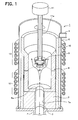
- a SiC single crystal manufacturing apparatus 1 according to a first embodiment of the present invention is described below with reference to FIG. 1 .
- the manufacturing apparatus 1 has an material gas inlet port 2 and an material gas outlet port 4.
- the material gas inlet port 2 is located at a bottom of the manufacturing apparatus 1, and the material gas outlet port 4 is located at an upper part of the manufacturing apparatus 1.
- a seed crystal 5, which is made from a SiC single crystal substrate, is placed in the manufacturing apparatus 1.
- a carrier gas and a material gas 3 for SiC are introduced into the manufacturing apparatus 1 through the material gas inlet port 2 and discharged from the manufacturing apparatus 1 through the material gas outlet port 4 so that a SiC single crystal 20 can be grown on the seed crystal 5.
- the material gas 3 contains both Si and C.
- the material gas 3 can be a gas mixture of a silane-based gas (e.g., silane) and a hydrocarbon-based gas (e.g., propane).
- the manufacturing apparatus 1 includes a vacuum container 6, a first heat insulator 7, a heating container 8, a base 9, a second heat insulator 10, a purge gas introduction mechanism 11, a first heating device 12, and a second heating device 13.
- the vacuum container 6 can be made of quartz glass.
- the vacuum container 6 has a cylindrical tube shape.
- the material gas inlet port 2 is located at a bottom of the vacuum container 6, and the material gas outlet port 4 is located at an upper part (e.g., upper part of a side wall) of the vacuum container 6.
- the carrier gas and the material gas 3 are introduced into an inner space of the vacuum container 6 through the material gas inlet port 2 and discharged from the inner space of the vacuum container 6 through the material gas outlet port 4.
- the vacuum container 6 is configured such that pressure in the inner space can be reduced by vacuuming the inner space.
- the first heat insulator 7 has a cylindrical tube shape and defines a material gas introduction pipe 7a communicating with the material gas inlet port 2.
- the first heat insulator 7 is coaxially arranged with the vacuum container 6.
- the first heat insulator 7 can be made of graphite.
- a surface of the first heat insulator 7 can be coated with a refractory (i.e., high-melting point) metal carbide such as tantalum carbide (TaC).
- the heating container 8 has a reaction chamber in which the SiC single crystal 20 is grown on a surface of the seed crystal 5.
- the heating container 8 can be made of graphite.
- a surface of the heating container 8 can be coated with a refractory metal carbide such as tantalum carbide (TaC).
- TaC tantalum carbide
- the heating container 8 is located on the upstream side of the base 9 in a flow direction of the material gas 3.
- the heating container 8 removes particles contained in the material gas 3 introduced from the material gas inlet port 2 and decomposes the material gas 3, before the material gas 3 reaches the seed crystal 5.
- the heating container 8 has a cylindrical tube shape. According to the first embodiment, the heating container 8 has a bottom with a gas introduction port 8a.
- the gas introduction port 8a communicates with the gas introduction pipe 7a of the first heat insulator 7 so that the material gas 3 flowing through the gas introduction pipe 7a can be introduced into the heating container 8 through the gas introduction port 8a.
- the base 9 is coaxially arranged with the heating container 8.
- the base 9 can be made of graphite.
- a surface of the base 9 can be coated with a refractory metal carbide such as tantalum carbide (TaC).
- TaC tantalum carbide
- the seed crystal 5 is mounted on the base 9, and the SiC single crystal 20 is grown on the surface of the seed crystal 5.
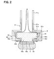
- the base 9 is described in detail below with reference to FIG. 2 .
- the base 9 includes a coupling portion 91 coupled to the purge gas introduction mechanism 11, a mounting portion 92 where the seed crystal 5 is mounted, and a holding portion 93 for holding the mounting portion 92.
- the coupling portion 91 has a first cylindrical tube 91a, a flange 91b, and a second cylindrical tube 91c.
- the first cylindrical tube 91a is coupled to a tip of a pipe member 11a of the purge gas introduction mechanism 11.
- the flange 91b extends in a radial outward direction of the first cylindrical tube 91a from an end of the first cylindrical tube 91a, opposite to an end coupled to the pipe member 11a.
- the second cylindrical tube 91c is formed on an outer region of a surface of the flange 91b, opposite to a surface where the first cylindrical tube 91a is formed.
- the first cylindrical tube 91a is coaxially arranged with the second cylindrical tube 91c.
- An inner diameter of the second cylindrical tube 91c is larger than an inner diameter of the first cylindrical tube 91a.
- the mounting portion 92 has a solid cylindrical shape with different diameters along its center axis.
- the mounting portion 92 includes a large diameter portion 92a and a small diameter portion 92b.
- a diameter of the small diameter portion 92b is smaller than a diameter of the large diameter portion 92a.
- the small diameter portion 92b is coaxially arranged with the large diameter portion 92a.
- Each of the diameters of the large diameter portion 92a and the small diameter portion 92b is smaller than the inner diameter of the second cylindrical tube 91c and an inner diameter of the holding portion 93 so that a clearance can be formed between the mounting portion 92 and each of the second cylindrical tube 91c and the holding portion 93.
- the clearance serves as a purge gas introduction path 94.
- the small diameter portion 92b is located under the large diameter portion 92a. A tip of the small diameter portion 92b extends beyond a lower edge of the holding portion 93.
- a mounting plate 92c is attached to the tip of the small diameter portion 92b and located outside the holding portion 93.
- a diameter of the mounting plate 92c is larger than the diameter of the small diameter portion 92b.
- the seed crystal 5 is mounted on the mounting plate 92c.
- Multiple supporting members 92d are arranged on a lower surface of the large diameter portion 92a at a regular interval around the small diameter portion 92b.
- the supporting members 92d are located between the large diameter portion 92a and the holding portion 93 to support the mounting portion 92 on the holding portion 93.
- Each of the supporting members 92d has a predetermined length.
- the mounting portion 92 is spaced from the holding portion 93 by the supporting members 92d so that the purge gas introduction path 94 can be formed.
- the holding portion 93 has a cylindrical tube portion 93a.
- the second cylindrical tube 91c of the coupling portion 91 is fitted into a first end of the cylindrical tube portion 93a.
- An adhesive is applied between the first end of the cylindrical tube portion 93a and the second cylindrical tube 91c so that the coupling portion 91 and the holding portion 93 can be fixed together.
- a second end of the cylindrical tube portion 93a is provided with a narrowed portion 93b that extends in a radial inward direction of the cylindrical tube portion 93a.
- An inner diameter of the narrowed portion 93b is smaller than an inner diameter of the cylindrical tube portion 93a.
- the supporting members 92d stand on the narrowed portion 93b to support the mounting portion 92 on the holding portion 93 in such a manner that the large diameter portion 92a is spaced from the narrowed portion 93b.
- the second heat insulator 10 surrounds the heating container 8 and the base 9 to lead the remainder of the material gas 3 introduced to the base 9 toward the material gas outlet port 4.
- the second heat insulator 10 is configured so that the remainder of the material gas 3 supplied to the seed crystal 5 can flow toward the material gas outlet port 4 through a clearance between the base 9 and the second heat insulator 10.
- the purge gas introduction mechanism 11 is configured to rotate and lift the pipe member 11a. Specifically, a first end of the pipe member 11a is connected to a surface of the base 9, opposite to the surface where the seed crystal 5 is mounted. A second end of the pipe member 11a is connected to the purge gas introduction mechanism 11. Thus, the purge gas introduction mechanism 11 can rotate and lift the pipe member 11a along with the base 9, the seed crystal 5, and the SiC single crystal 20.
- the purge gas introduction mechanism 11 keeps a growth face of the SiC single crystal 20 at a temperature suitable for growth of the SiC single crystal 20 by rotating and lifting the pipe member 11a according to the growth of the SiC single crystal 20.
- the purge gas introduction mechanism 11 introduces a purge gas into the pipe member 11a to supply the purge gas to the base 9, which is connected to the pipe member 11a.
- the purge gas can be an inert gas (e.g., Ar, He), an etching gas (e.g., H 2 , HC1), or a mixture gas of the inert gas and the etching gas.
- the purge gas that is supplied from the purge gas introduction mechanism 11 to the base 9 is discharged from an outer edge of the seed crystal 5 in a radial outward direction with respect to the center axis of the base 9.
- Each of the first heating device 12 and the second heating device 13 surrounds the vacuum container 6.
- each of the first heating device 12 and the second heating device 13 can include a heat-generating induction coil, a heater, or the like.
- the first heating device 12 is located at a position corresponding to a lower part of the heating container 8, and the second heating device 13 is located at a position corresponding to the base 9.
- the first heating device 12 and the second heating device 13 are independently controlled so that the growth face of the SiC single crystal 20 can be adjusted to the temperature suitable for the growth of the SiC single crystal 20.
- the seed crystal 5 is mounted on the base 9. Then, the first heating device 12 and the second heating device 13 are controlled to generate a predetermined temperature distribution in the heating container 8.
- the predetermined temperature distribution is set so that the material gas 3 can be recrystallized at the surface of the seed crystal 5 to grow the SiC single crystal 20 on the surface of the seed crystal 5. Further, the predetermined temperature distribution is set so that the recrystallization rate can be less than a sublimation rate in the heating container 8.
- the vacuum container 6 is kept at a predetermined pressure, and the material gas 3 is introduced into the vacuum container 6 through the gas introduction pipe 7a.
- a carrier gas e.g., inert gas such as Ar, He
- an etching gas e.g., H 2 , HC1
- the material gas 3 is supplied to the seed crystal 5 so that the SiC single crystal 20 can be grown on the seed crystal 5.
- the purge gas introduction mechanism 11 introduces the purge gas into the pipe member 11a.
- the purge gas is supplied to the seed crystal 5 from the back side of the seed crystal 5 through the purge gas introduction path 94 and then discharged from the outer edge of the seed crystal 5 in the radial outward direction with respect to the center axis of the base 9.
- Such a flow of the purge gas reduces or prevents formation of a polycrystal on a portion of the base 9 around the seed crystal 5, for example, the lower surface of the holding portion 93 and the lower surface of the large diameter portion 92a.
- the SiC single crystal 20 can be grown long without loss of quality of the outer edge of the SiC single crystal 20.
- the lower surface of the holding portion 93 is parallel to the horizontal plane.
- the small diameter portion 92b of the mounting portion 92 extends downward beyond the narrowed portion 93b, and the mounting plate 92c having the larger diameter than the small diameter portion 92b is attached to the tip of the small diameter portion 92b.
- an outlet (i.e., exit) of the purge gas introduction path 94 faces in the radial outward direction with respect to the center axis of the base 9 so that the purge gas can be discharged from the base 9 in the radial outward direction. Accordingly, the discharged purge gas flows along the lower surface of the holding portion 93 so that the formation of the polycrystal on the lower surface of the holding portion 93 can be reduced or prevented.
- the purge gas is supplied to the seed crystal 5 from the back side of the seed crystal 5 and discharged from the outer edge of the seed crystal 5 in the radial outward direction with respect to the center axis of the base 9.
- the flow of the purge gas reduces or prevents formation of the polycrystal on the portion of the base 9 around the seed crystal 5, for example, the lower surface of the holding portion 93 and the lower surface of the large diameter portion 92a.
- the SiC single crystal 20 can be grown long without loss of quality of the outer edge of the SiC single crystal 20.
- a second embodiment of the present invention is described below with reference to FIG. 3 .
- the second embodiment differs from the first embodiment in the shape of the base 9.
- FIG. 3 is a diagram illustrating a partial enlarged cross-sectional view of a base 9 of a SiC single crystal manufacturing apparatus 1 according to the second embodiment.
- the lower surface of the holding portion 93 of the base 9 is tapered so that the diameter of the narrowed portion 93b with respect to the center axis of the base 9 can be increased in the direction of growth of the SiC single crystal 20.
- the lower surface of the holding portion 93 is tapered.
- the SiC single crystal 20 is grown along the tapered lower surface of the holding portion 93 so that the diameter of the SiC single crystal 20 can be increased.
- the purge gas flows along the tapered lower surface of the holding portion 93, the formation of the polycrystal on the tapered lower surface of the holding portion 93 can be prevented or reduced.
- a third embodiment of the present invention is described below with reference to FIG. 4 .
- the third embodiment differs from the first embodiment in the shape of the base 9.
- FIG. 4 is a diagram illustrating a partial enlarged cross-sectional view of a base 9 of a SiC single crystal manufacturing apparatus 1 according to the third embodiment.
- the base 9 has a cylindrical shape with different diameters along its center axis.
- the base 9 includes a large diameter portion 95a and a small diameter portion 95b.
- a diameter of the small diameter portion 95b is smaller than a diameter of the large diameter portion 95a.
- the small diameter portion 95b is coaxially arranged with the large diameter portion 95a and located under the large diameter portion 95a.
- the seed crystal 5 is mounted on a tip of the small diameter portion 95b. That is, the tip of the small diameter portion 95b serves as the mounting plate 92c.
- the base 9 has a purge gas introduction path 95c.
- the purge gas introduction path 95c extends from the back side of the large diameter portion 95a to the small diameter portion 95b and then extends through the small diameter portion 95b in the radial outward direction with respect to the center axis of the base 9. Through the purge gas introduction path 95c, the purge gas is supplied to the seed crystal 5 from the back side of the seed crystal 5 and then discharged from the outer edge of the seed crystal 5 in the radial outward direction.
- the base 9 has the purge gas introduction path 95c that extends from the back side of the large diameter portion 95a to the small diameter portion 95b and then extends through the small diameter portion 95b in the radial outward direction.
- the flow of the purge gas reduces or prevents formation of the polycrystal on the portion of the base 9 around the seed crystal 5, for example, the lower surface of the large diameter portion 95a.
- the SiC single crystal 20 can be grown long without loss of quality of the outer edge of the SiC single crystal 20.
- a fourth embodiment of the present invention is described below with reference to FIG. 5 .
- the fourth embodiment is similar to the third embodiment.
- a difference between the third embodiment and the fourth embodiment is as follows.
- FIG. 5 is a diagram illustrating a partial enlarged cross-sectional view of a base 9 of a SiC single crystal manufacturing apparatus 1 according to the fourth embodiment.
- the base 9 further has a canopy portion 95d in addition to the large diameter portion 95a, the small diameter portion 95b, and the purge gas introduction path 95c.
- the canopy portion 95d covers the lower surface of the large diameter portion 95a and the side surface of the small diameter portion 95b. Specifically, the canopy portion 95d extends from the lower surface of the large diameter portion 95a and is bent toward the side surface of the small diameter portion 95b.
- a first end of the canopy portion 95d is joined to the large diameter portion 95a, and a second end of the canopy portion 95d is spaced from the small diameter portion 95b.
- the purge gas flowing through the purge gas introduction path 95c is discharged from the base 9 through a clearance between the canopy portion 95d and the small diameter portion 95b so that the discharged purge gas can flow to the outer edge of the seed crystal 5.
- the base 9 further has the canopy portion 95d that covers the lower surface of the large diameter portion 95a and the side surface of the small diameter portion 95b.
- the flow of the purge gas reduces or prevents formation of the polycrystal on the portion of the base 9 around the seed crystal 5, for example, the lower surface of the large diameter portion 95a and the lower surface of the canopy portion 95d.
- the surface of the base 9 be coated with a refractory metal carbide such as tantalum carbide (TaC).
- a refractory metal carbide such as tantalum carbide (TaC).
- TaC tantalum carbide
- the surface of the base 9 is protected from thermal etching and the etching gas so that formation of the polycrystal on the surface of the base 9 can be reduced or prevented.
- the lower surface of the narrowed portion 93b of the holding portion 93 be coated with a refractory metal carbide.
- the purge gas can be an inert gas, an etching gas, a dopant gas for silicon carbide, or a mixture gas of at least two of the inert gas, the etching gas, and the dopant gas.
- the dopant gas can be a nitrogen (N 2 ) gas.
Landscapes
- Chemical & Material Sciences (AREA)
- Engineering & Computer Science (AREA)
- Crystallography & Structural Chemistry (AREA)
- Materials Engineering (AREA)
- Metallurgy (AREA)
- Organic Chemistry (AREA)
- Chemical Kinetics & Catalysis (AREA)
- General Chemical & Material Sciences (AREA)
- Inorganic Chemistry (AREA)
- Crystals, And After-Treatments Of Crystals (AREA)
Applications Claiming Priority (1)
| Application Number | Priority Date | Filing Date | Title |
|---|---|---|---|
| JP2010280309A JP5287840B2 (ja) | 2010-12-16 | 2010-12-16 | 炭化珪素単結晶の製造装置 |
Publications (3)
| Publication Number | Publication Date |
|---|---|
| EP2465980A2 true EP2465980A2 (de) | 2012-06-20 |
| EP2465980A3 EP2465980A3 (de) | 2013-11-27 |
| EP2465980B1 EP2465980B1 (de) | 2017-04-26 |
Family
ID=45318955
Family Applications (1)
| Application Number | Title | Priority Date | Filing Date |
|---|---|---|---|
| EP11192942.8A Active EP2465980B1 (de) | 2010-12-16 | 2011-12-12 | Vorrichtung und Verfahren zur Herstellung eines Siliciumcarbid-Einkristalls |
Country Status (5)
| Country | Link |
|---|---|
| US (1) | US9328431B2 (de) |
| EP (1) | EP2465980B1 (de) |
| JP (1) | JP5287840B2 (de) |
| KR (1) | KR101437378B1 (de) |
| CN (2) | CN106948007A (de) |
Families Citing this family (6)
| Publication number | Priority date | Publication date | Assignee | Title |
|---|---|---|---|---|
| JP6052051B2 (ja) * | 2013-05-16 | 2016-12-27 | 株式会社デンソー | 炭化珪素単結晶の製造装置 |
| US9580837B2 (en) | 2014-09-03 | 2017-02-28 | Ii-Vi Incorporated | Method for silicon carbide crystal growth by reacting elemental silicon vapor with a porous carbon solid source material |
| KR102762144B1 (ko) * | 2020-09-18 | 2025-02-03 | 주식회사 엘지화학 | 탄화규소 단결정의 제조 장치 |
| AT524251B1 (de) * | 2020-09-28 | 2023-04-15 | Ebner Ind Ofenbau | Vorrichtung zum Züchten von Einkristallen |
| JP7639335B2 (ja) * | 2020-12-28 | 2025-03-05 | 株式会社レゾナック | 炭化珪素単結晶製造装置および炭化珪素単結晶の製造方法 |
| TWI789915B (zh) | 2021-09-15 | 2023-01-11 | 國家中山科學研究院 | 提升碳化矽單晶成長良率之方法 |
Citations (1)
| Publication number | Priority date | Publication date | Assignee | Title |
|---|---|---|---|---|
| JP2007176718A (ja) | 2005-12-27 | 2007-07-12 | Matsushita Electric Ind Co Ltd | 炭化珪素単結晶の製造方法及び製造装置 |
Family Cites Families (10)
| Publication number | Priority date | Publication date | Assignee | Title |
|---|---|---|---|---|
| EP0933450B1 (de) * | 1998-01-19 | 2002-04-17 | Sumitomo Electric Industries, Ltd. | Verfahren und Vorrichtung zur Herstellung eines SiC-Einkristalles |
| JP4742448B2 (ja) * | 2001-06-06 | 2011-08-10 | 株式会社デンソー | 炭化珪素単結晶の製造方法及び製造装置 |
| DE602004001802T3 (de) * | 2003-04-24 | 2012-01-26 | Norstel Ab | Vorrichtung und Verfahren zur Herstellung von Einkristallen durch Dampfphasenabscheidung |
| ITMI20031196A1 (it) * | 2003-06-13 | 2004-12-14 | Lpe Spa | Sistema per crescere cristalli di carburo di silicio |
| JP4150642B2 (ja) * | 2003-08-04 | 2008-09-17 | 株式会社デンソー | 単結晶の成長方法および成長装置 |
| JP4225296B2 (ja) * | 2005-06-20 | 2009-02-18 | トヨタ自動車株式会社 | 炭化珪素単結晶の製造方法 |
| WO2008014434A2 (en) * | 2006-07-28 | 2008-01-31 | Caracal, Inc. | Crystal growth method and reactor design |
| WO2008088838A1 (en) * | 2007-01-17 | 2008-07-24 | Crystal Is, Inc. | Defect reduction in seeded aluminum nitride crystal growth |
| JP4277926B1 (ja) * | 2007-11-27 | 2009-06-10 | トヨタ自動車株式会社 | 炭化珪素単結晶の成長法 |
| JP5212455B2 (ja) | 2010-12-16 | 2013-06-19 | 株式会社デンソー | 炭化珪素単結晶の製造装置 |
-
2010
- 2010-12-16 JP JP2010280309A patent/JP5287840B2/ja active Active
-
2011
- 2011-12-12 EP EP11192942.8A patent/EP2465980B1/de active Active
- 2011-12-14 KR KR1020110134710A patent/KR101437378B1/ko active Active
- 2011-12-14 US US13/325,233 patent/US9328431B2/en active Active
- 2011-12-16 CN CN201610862561.1A patent/CN106948007A/zh active Pending
- 2011-12-16 CN CN2011104317479A patent/CN102534795A/zh active Pending
Patent Citations (1)
| Publication number | Priority date | Publication date | Assignee | Title |
|---|---|---|---|---|
| JP2007176718A (ja) | 2005-12-27 | 2007-07-12 | Matsushita Electric Ind Co Ltd | 炭化珪素単結晶の製造方法及び製造装置 |
Also Published As
| Publication number | Publication date |
|---|---|
| KR101437378B1 (ko) | 2014-09-05 |
| CN106948007A (zh) | 2017-07-14 |
| JP5287840B2 (ja) | 2013-09-11 |
| EP2465980B1 (de) | 2017-04-26 |
| US9328431B2 (en) | 2016-05-03 |
| KR20120067943A (ko) | 2012-06-26 |
| JP2012126613A (ja) | 2012-07-05 |
| CN102534795A (zh) | 2012-07-04 |
| US20120152165A1 (en) | 2012-06-21 |
| EP2465980A3 (de) | 2013-11-27 |
Similar Documents
| Publication | Publication Date | Title |
|---|---|---|
| EP2465979B1 (de) | Verfahren zur Herstellung eines Siliziumcarbid-Einkristalls | |
| EP2465980A2 (de) | Vorrichtung und Verfahren zur Herstellung eines Siliciumcarbid-Einkristalls | |
| US9017483B2 (en) | Susceptor for vapor phase epitaxial growth device | |
| US20110155048A1 (en) | Manufacturing apparatus and manufacturing method of silicon carbide single crystal | |
| CN112334607B (zh) | 碳化硅单晶及其制造方法 | |
| CN111033692B (zh) | 气相生长方法 | |
| JP2023121839A (ja) | SiCエピタキシャルウェハ | |
| US20210040645A1 (en) | Silicon carbide single crystal manufacturing apparatus, and manufacturing method of silicon carbide single crystal | |
| JP2015198213A (ja) | エピタキシャル炭化珪素ウェハの製造方法及びそれに用いる炭化珪素単結晶基板のホルダー | |
| JP5648604B2 (ja) | 炭化珪素単結晶製造装置 | |
| JP6052051B2 (ja) | 炭化珪素単結晶の製造装置 | |
| JP5831339B2 (ja) | 炭化珪素単結晶の製造方法 | |
| JP5811012B2 (ja) | 炭化珪素単結晶の製造装置および製造方法 | |
| JP5482669B2 (ja) | 炭化珪素単結晶の製造装置 | |
| JP6187372B2 (ja) | 炭化珪素単結晶製造装置 | |
| JP2002134425A (ja) | 気相成長方法 |
Legal Events
| Date | Code | Title | Description |
|---|---|---|---|
| PUAI | Public reference made under article 153(3) epc to a published international application that has entered the european phase |
Free format text: ORIGINAL CODE: 0009012 |
|
| AK | Designated contracting states |
Kind code of ref document: A2 Designated state(s): AL AT BE BG CH CY CZ DE DK EE ES FI FR GB GR HR HU IE IS IT LI LT LU LV MC MK MT NL NO PL PT RO RS SE SI SK SM TR |
|
| AX | Request for extension of the european patent |
Extension state: BA ME |
|
| PUAL | Search report despatched |
Free format text: ORIGINAL CODE: 0009013 |
|
| AK | Designated contracting states |
Kind code of ref document: A3 Designated state(s): AL AT BE BG CH CY CZ DE DK EE ES FI FR GB GR HR HU IE IS IT LI LT LU LV MC MK MT NL NO PL PT RO RS SE SI SK SM TR |
|
| AX | Request for extension of the european patent |
Extension state: BA ME |
|
| RIC1 | Information provided on ipc code assigned before grant |
Ipc: C30B 25/12 20060101ALI20131021BHEP Ipc: C30B 25/16 20060101ALI20131021BHEP Ipc: C30B 29/36 20060101ALI20131021BHEP Ipc: C30B 25/14 20060101AFI20131021BHEP |
|
| 17P | Request for examination filed |
Effective date: 20140403 |
|
| RBV | Designated contracting states (corrected) |
Designated state(s): AL AT BE BG CH CY CZ DE DK EE ES FI FR GB GR HR HU IE IS IT LI LT LU LV MC MK MT NL NO PL PT RO RS SE SI SK SM TR |
|
| 17Q | First examination report despatched |
Effective date: 20160504 |
|
| GRAP | Despatch of communication of intention to grant a patent |
Free format text: ORIGINAL CODE: EPIDOSNIGR1 |
|
| STAA | Information on the status of an ep patent application or granted ep patent |
Free format text: STATUS: GRANT OF PATENT IS INTENDED |
|
| INTG | Intention to grant announced |
Effective date: 20161102 |
|
| GRAS | Grant fee paid |
Free format text: ORIGINAL CODE: EPIDOSNIGR3 |
|
| GRAA | (expected) grant |
Free format text: ORIGINAL CODE: 0009210 |
|
| STAA | Information on the status of an ep patent application or granted ep patent |
Free format text: STATUS: THE PATENT HAS BEEN GRANTED |
|
| AK | Designated contracting states |
Kind code of ref document: B1 Designated state(s): AL AT BE BG CH CY CZ DE DK EE ES FI FR GB GR HR HU IE IS IT LI LT LU LV MC MK MT NL NO PL PT RO RS SE SI SK SM TR |
|
| REG | Reference to a national code |
Ref country code: GB Ref legal event code: FG4D |
|
| REG | Reference to a national code |
Ref country code: CH Ref legal event code: EP |
|
| REG | Reference to a national code |
Ref country code: AT Ref legal event code: REF Ref document number: 887965 Country of ref document: AT Kind code of ref document: T Effective date: 20170515 |
|
| REG | Reference to a national code |
Ref country code: IE Ref legal event code: FG4D |
|
| REG | Reference to a national code |
Ref country code: DE Ref legal event code: R096 Ref document number: 602011037302 Country of ref document: DE |
|
| REG | Reference to a national code |
Ref country code: SE Ref legal event code: TRGR |
|
| REG | Reference to a national code |
Ref country code: NL Ref legal event code: MP Effective date: 20170426 |
|
| REG | Reference to a national code |
Ref country code: LT Ref legal event code: MG4D |
|
| REG | Reference to a national code |
Ref country code: AT Ref legal event code: MK05 Ref document number: 887965 Country of ref document: AT Kind code of ref document: T Effective date: 20170426 |
|
| PG25 | Lapsed in a contracting state [announced via postgrant information from national office to epo] |
Ref country code: NL Free format text: LAPSE BECAUSE OF FAILURE TO SUBMIT A TRANSLATION OF THE DESCRIPTION OR TO PAY THE FEE WITHIN THE PRESCRIBED TIME-LIMIT Effective date: 20170426 |
|
| PG25 | Lapsed in a contracting state [announced via postgrant information from national office to epo] |
Ref country code: LT Free format text: LAPSE BECAUSE OF FAILURE TO SUBMIT A TRANSLATION OF THE DESCRIPTION OR TO PAY THE FEE WITHIN THE PRESCRIBED TIME-LIMIT Effective date: 20170426 Ref country code: FI Free format text: LAPSE BECAUSE OF FAILURE TO SUBMIT A TRANSLATION OF THE DESCRIPTION OR TO PAY THE FEE WITHIN THE PRESCRIBED TIME-LIMIT Effective date: 20170426 Ref country code: HR Free format text: LAPSE BECAUSE OF FAILURE TO SUBMIT A TRANSLATION OF THE DESCRIPTION OR TO PAY THE FEE WITHIN THE PRESCRIBED TIME-LIMIT Effective date: 20170426 Ref country code: GR Free format text: LAPSE BECAUSE OF FAILURE TO SUBMIT A TRANSLATION OF THE DESCRIPTION OR TO PAY THE FEE WITHIN THE PRESCRIBED TIME-LIMIT Effective date: 20170727 Ref country code: AT Free format text: LAPSE BECAUSE OF FAILURE TO SUBMIT A TRANSLATION OF THE DESCRIPTION OR TO PAY THE FEE WITHIN THE PRESCRIBED TIME-LIMIT Effective date: 20170426 Ref country code: ES Free format text: LAPSE BECAUSE OF FAILURE TO SUBMIT A TRANSLATION OF THE DESCRIPTION OR TO PAY THE FEE WITHIN THE PRESCRIBED TIME-LIMIT Effective date: 20170426 Ref country code: NO Free format text: LAPSE BECAUSE OF FAILURE TO SUBMIT A TRANSLATION OF THE DESCRIPTION OR TO PAY THE FEE WITHIN THE PRESCRIBED TIME-LIMIT Effective date: 20170726 |
|
| PG25 | Lapsed in a contracting state [announced via postgrant information from national office to epo] |
Ref country code: IS Free format text: LAPSE BECAUSE OF FAILURE TO SUBMIT A TRANSLATION OF THE DESCRIPTION OR TO PAY THE FEE WITHIN THE PRESCRIBED TIME-LIMIT Effective date: 20170826 Ref country code: PL Free format text: LAPSE BECAUSE OF FAILURE TO SUBMIT A TRANSLATION OF THE DESCRIPTION OR TO PAY THE FEE WITHIN THE PRESCRIBED TIME-LIMIT Effective date: 20170426 Ref country code: BG Free format text: LAPSE BECAUSE OF FAILURE TO SUBMIT A TRANSLATION OF THE DESCRIPTION OR TO PAY THE FEE WITHIN THE PRESCRIBED TIME-LIMIT Effective date: 20170726 Ref country code: LV Free format text: LAPSE BECAUSE OF FAILURE TO SUBMIT A TRANSLATION OF THE DESCRIPTION OR TO PAY THE FEE WITHIN THE PRESCRIBED TIME-LIMIT Effective date: 20170426 Ref country code: RS Free format text: LAPSE BECAUSE OF FAILURE TO SUBMIT A TRANSLATION OF THE DESCRIPTION OR TO PAY THE FEE WITHIN THE PRESCRIBED TIME-LIMIT Effective date: 20170426 |
|
| REG | Reference to a national code |
Ref country code: DE Ref legal event code: R097 Ref document number: 602011037302 Country of ref document: DE |
|
| PG25 | Lapsed in a contracting state [announced via postgrant information from national office to epo] |
Ref country code: EE Free format text: LAPSE BECAUSE OF FAILURE TO SUBMIT A TRANSLATION OF THE DESCRIPTION OR TO PAY THE FEE WITHIN THE PRESCRIBED TIME-LIMIT Effective date: 20170426 Ref country code: SK Free format text: LAPSE BECAUSE OF FAILURE TO SUBMIT A TRANSLATION OF THE DESCRIPTION OR TO PAY THE FEE WITHIN THE PRESCRIBED TIME-LIMIT Effective date: 20170426 Ref country code: RO Free format text: LAPSE BECAUSE OF FAILURE TO SUBMIT A TRANSLATION OF THE DESCRIPTION OR TO PAY THE FEE WITHIN THE PRESCRIBED TIME-LIMIT Effective date: 20170426 Ref country code: DK Free format text: LAPSE BECAUSE OF FAILURE TO SUBMIT A TRANSLATION OF THE DESCRIPTION OR TO PAY THE FEE WITHIN THE PRESCRIBED TIME-LIMIT Effective date: 20170426 Ref country code: CZ Free format text: LAPSE BECAUSE OF FAILURE TO SUBMIT A TRANSLATION OF THE DESCRIPTION OR TO PAY THE FEE WITHIN THE PRESCRIBED TIME-LIMIT Effective date: 20170426 |
|
| PG25 | Lapsed in a contracting state [announced via postgrant information from national office to epo] |
Ref country code: SM Free format text: LAPSE BECAUSE OF FAILURE TO SUBMIT A TRANSLATION OF THE DESCRIPTION OR TO PAY THE FEE WITHIN THE PRESCRIBED TIME-LIMIT Effective date: 20170426 |
|
| PLBE | No opposition filed within time limit |
Free format text: ORIGINAL CODE: 0009261 |
|
| STAA | Information on the status of an ep patent application or granted ep patent |
Free format text: STATUS: NO OPPOSITION FILED WITHIN TIME LIMIT |
|
| 26N | No opposition filed |
Effective date: 20180129 |
|
| PG25 | Lapsed in a contracting state [announced via postgrant information from national office to epo] |
Ref country code: SI Free format text: LAPSE BECAUSE OF FAILURE TO SUBMIT A TRANSLATION OF THE DESCRIPTION OR TO PAY THE FEE WITHIN THE PRESCRIBED TIME-LIMIT Effective date: 20170426 |
|
| REG | Reference to a national code |
Ref country code: CH Ref legal event code: PL |
|
| GBPC | Gb: european patent ceased through non-payment of renewal fee |
Effective date: 20171212 |
|
| REG | Reference to a national code |
Ref country code: IE Ref legal event code: MM4A |
|
| PG25 | Lapsed in a contracting state [announced via postgrant information from national office to epo] |
Ref country code: LU Free format text: LAPSE BECAUSE OF NON-PAYMENT OF DUE FEES Effective date: 20171212 Ref country code: MT Free format text: LAPSE BECAUSE OF NON-PAYMENT OF DUE FEES Effective date: 20171212 |
|
| REG | Reference to a national code |
Ref country code: FR Ref legal event code: ST Effective date: 20180831 |
|
| REG | Reference to a national code |
Ref country code: BE Ref legal event code: MM Effective date: 20171231 |
|
| PG25 | Lapsed in a contracting state [announced via postgrant information from national office to epo] |
Ref country code: IE Free format text: LAPSE BECAUSE OF NON-PAYMENT OF DUE FEES Effective date: 20171212 Ref country code: FR Free format text: LAPSE BECAUSE OF NON-PAYMENT OF DUE FEES Effective date: 20180102 |
|
| PG25 | Lapsed in a contracting state [announced via postgrant information from national office to epo] |
Ref country code: CH Free format text: LAPSE BECAUSE OF NON-PAYMENT OF DUE FEES Effective date: 20171231 Ref country code: GB Free format text: LAPSE BECAUSE OF NON-PAYMENT OF DUE FEES Effective date: 20171212 Ref country code: LI Free format text: LAPSE BECAUSE OF NON-PAYMENT OF DUE FEES Effective date: 20171231 Ref country code: BE Free format text: LAPSE BECAUSE OF NON-PAYMENT OF DUE FEES Effective date: 20171231 |
|
| PG25 | Lapsed in a contracting state [announced via postgrant information from national office to epo] |
Ref country code: MC Free format text: LAPSE BECAUSE OF FAILURE TO SUBMIT A TRANSLATION OF THE DESCRIPTION OR TO PAY THE FEE WITHIN THE PRESCRIBED TIME-LIMIT Effective date: 20170426 Ref country code: HU Free format text: LAPSE BECAUSE OF FAILURE TO SUBMIT A TRANSLATION OF THE DESCRIPTION OR TO PAY THE FEE WITHIN THE PRESCRIBED TIME-LIMIT; INVALID AB INITIO Effective date: 20111212 |
|
| PG25 | Lapsed in a contracting state [announced via postgrant information from national office to epo] |
Ref country code: CY Free format text: LAPSE BECAUSE OF NON-PAYMENT OF DUE FEES Effective date: 20170426 |
|
| PG25 | Lapsed in a contracting state [announced via postgrant information from national office to epo] |
Ref country code: MK Free format text: LAPSE BECAUSE OF FAILURE TO SUBMIT A TRANSLATION OF THE DESCRIPTION OR TO PAY THE FEE WITHIN THE PRESCRIBED TIME-LIMIT Effective date: 20170426 |
|
| PG25 | Lapsed in a contracting state [announced via postgrant information from national office to epo] |
Ref country code: TR Free format text: LAPSE BECAUSE OF FAILURE TO SUBMIT A TRANSLATION OF THE DESCRIPTION OR TO PAY THE FEE WITHIN THE PRESCRIBED TIME-LIMIT Effective date: 20170426 |
|
| PG25 | Lapsed in a contracting state [announced via postgrant information from national office to epo] |
Ref country code: PT Free format text: LAPSE BECAUSE OF FAILURE TO SUBMIT A TRANSLATION OF THE DESCRIPTION OR TO PAY THE FEE WITHIN THE PRESCRIBED TIME-LIMIT Effective date: 20170426 |
|
| PG25 | Lapsed in a contracting state [announced via postgrant information from national office to epo] |
Ref country code: AL Free format text: LAPSE BECAUSE OF FAILURE TO SUBMIT A TRANSLATION OF THE DESCRIPTION OR TO PAY THE FEE WITHIN THE PRESCRIBED TIME-LIMIT Effective date: 20170426 |
|
| PGFP | Annual fee paid to national office [announced via postgrant information from national office to epo] |
Ref country code: DE Payment date: 20251211 Year of fee payment: 15 |
|
| PGFP | Annual fee paid to national office [announced via postgrant information from national office to epo] |
Ref country code: IT Payment date: 20251223 Year of fee payment: 15 |
|
| PGFP | Annual fee paid to national office [announced via postgrant information from national office to epo] |
Ref country code: SE Payment date: 20251219 Year of fee payment: 15 |