EP2467976B1 - Synchronisationsverteilung in mikrowellen-backhaul-netzwerken - Google Patents
Synchronisationsverteilung in mikrowellen-backhaul-netzwerken Download PDFInfo
- Publication number
- EP2467976B1 EP2467976B1 EP10810727.7A EP10810727A EP2467976B1 EP 2467976 B1 EP2467976 B1 EP 2467976B1 EP 10810727 A EP10810727 A EP 10810727A EP 2467976 B1 EP2467976 B1 EP 2467976B1
- Authority
- EP
- European Patent Office
- Prior art keywords
- synchronization
- frame
- clock
- child node
- clock signal
- Prior art date
- Legal status (The legal status is an assumption and is not a legal conclusion. Google has not performed a legal analysis and makes no representation as to the accuracy of the status listed.)
- Active
Links
Images




Classifications
-
- H—ELECTRICITY
- H04—ELECTRIC COMMUNICATION TECHNIQUE
- H04W—WIRELESS COMMUNICATION NETWORKS
- H04W56/00—Synchronisation arrangements
- H04W56/001—Synchronization between nodes
- H04W56/0015—Synchronization between nodes one node acting as a reference for the others
-
- H—ELECTRICITY
- H03—ELECTRONIC CIRCUITRY
- H03L—AUTOMATIC CONTROL, STARTING, SYNCHRONISATION OR STABILISATION OF GENERATORS OF ELECTRONIC OSCILLATIONS OR PULSES
- H03L7/00—Automatic control of frequency or phase; Synchronisation
- H03L7/06—Automatic control of frequency or phase; Synchronisation using a reference signal applied to a frequency- or phase-locked loop
- H03L7/08—Details of the phase-locked loop
-
- H—ELECTRICITY
- H03—ELECTRONIC CIRCUITRY
- H03L—AUTOMATIC CONTROL, STARTING, SYNCHRONISATION OR STABILISATION OF GENERATORS OF ELECTRONIC OSCILLATIONS OR PULSES
- H03L7/00—Automatic control of frequency or phase; Synchronisation
- H03L7/06—Automatic control of frequency or phase; Synchronisation using a reference signal applied to a frequency- or phase-locked loop
- H03L7/16—Indirect frequency synthesis, i.e. generating a desired one of a number of predetermined frequencies using a frequency- or phase-locked loop
- H03L7/18—Indirect frequency synthesis, i.e. generating a desired one of a number of predetermined frequencies using a frequency- or phase-locked loop using a frequency divider or counter in the loop
-
- H—ELECTRICITY
- H04—ELECTRIC COMMUNICATION TECHNIQUE
- H04J—MULTIPLEX COMMUNICATION
- H04J3/00—Time-division multiplex systems
- H04J3/02—Details
- H04J3/06—Synchronising arrangements
- H04J3/0602—Systems characterised by the synchronising information used
-
- H—ELECTRICITY
- H04—ELECTRIC COMMUNICATION TECHNIQUE
- H04J—MULTIPLEX COMMUNICATION
- H04J3/00—Time-division multiplex systems
- H04J3/02—Details
- H04J3/06—Synchronising arrangements
- H04J3/0602—Systems characterised by the synchronising information used
- H04J3/0617—Systems characterised by the synchronising information used the synchronising signal being characterised by the frequency or phase
-
- H—ELECTRICITY
- H04—ELECTRIC COMMUNICATION TECHNIQUE
- H04J—MULTIPLEX COMMUNICATION
- H04J3/00—Time-division multiplex systems
- H04J3/02—Details
- H04J3/06—Synchronising arrangements
- H04J3/0635—Clock or time synchronisation in a network
- H04J3/0638—Clock or time synchronisation among nodes; Internode synchronisation
-
- H—ELECTRICITY
- H04—ELECTRIC COMMUNICATION TECHNIQUE
- H04J—MULTIPLEX COMMUNICATION
- H04J3/00—Time-division multiplex systems
- H04J3/02—Details
- H04J3/06—Synchronising arrangements
- H04J3/0635—Clock or time synchronisation in a network
- H04J3/0638—Clock or time synchronisation among nodes; Internode synchronisation
- H04J3/0647—Synchronisation among TDM nodes
-
- H—ELECTRICITY
- H04—ELECTRIC COMMUNICATION TECHNIQUE
- H04J—MULTIPLEX COMMUNICATION
- H04J3/00—Time-division multiplex systems
- H04J3/02—Details
- H04J3/06—Synchronising arrangements
- H04J3/0635—Clock or time synchronisation in a network
- H04J3/0638—Clock or time synchronisation among nodes; Internode synchronisation
- H04J3/0647—Synchronisation among TDM nodes
- H04J3/065—Synchronisation among TDM nodes using timestamps
-
- H—ELECTRICITY
- H04—ELECTRIC COMMUNICATION TECHNIQUE
- H04J—MULTIPLEX COMMUNICATION
- H04J3/00—Time-division multiplex systems
- H04J3/02—Details
- H04J3/06—Synchronising arrangements
- H04J3/0635—Clock or time synchronisation in a network
- H04J3/0638—Clock or time synchronisation among nodes; Internode synchronisation
- H04J3/0658—Clock or time synchronisation among packet nodes
-
- H—ELECTRICITY
- H04—ELECTRIC COMMUNICATION TECHNIQUE
- H04J—MULTIPLEX COMMUNICATION
- H04J3/00—Time-division multiplex systems
- H04J3/02—Details
- H04J3/06—Synchronising arrangements
- H04J3/0635—Clock or time synchronisation in a network
- H04J3/0679—Clock or time synchronisation in a network by determining clock distribution path in a network
-
- H—ELECTRICITY
- H03—ELECTRONIC CIRCUITRY
- H03L—AUTOMATIC CONTROL, STARTING, SYNCHRONISATION OR STABILISATION OF GENERATORS OF ELECTRONIC OSCILLATIONS OR PULSES
- H03L2207/00—Indexing scheme relating to automatic control of frequency or phase and to synchronisation
- H03L2207/50—All digital phase-locked loop
-
- H—ELECTRICITY
- H04—ELECTRIC COMMUNICATION TECHNIQUE
- H04J—MULTIPLEX COMMUNICATION
- H04J3/00—Time-division multiplex systems
- H04J3/02—Details
- H04J3/06—Synchronising arrangements
- H04J3/0635—Clock or time synchronisation in a network
- H04J3/0638—Clock or time synchronisation among nodes; Internode synchronisation
- H04J3/0641—Change of the master or reference, e.g. take-over or failure of the master
-
- H—ELECTRICITY
- H04—ELECTRIC COMMUNICATION TECHNIQUE
- H04J—MULTIPLEX COMMUNICATION
- H04J3/00—Time-division multiplex systems
- H04J3/02—Details
- H04J3/06—Synchronising arrangements
- H04J3/0635—Clock or time synchronisation in a network
- H04J3/0685—Clock or time synchronisation in a node; Intranode synchronisation
- H04J3/0688—Change of the master or reference, e.g. take-over or failure of the master
Definitions
- the present invention generally relates to data synchronization. More particularly, the invention relates to data synchronization across a network.
- Ethernet is regarded as the unifying transport layer of choice for network convergence. Ethernet backhaul will become universal over time and may replace traditional TDM backhaul.
- Ethernet will be introduced on the back of existing TDM network connections given the huge investment in TDM network infrastructure. This will typically involve gradual migration using data overlay, with a decision at some future point to change to an all packet-based network.
- PDH Plesiochronous Digital Hierarchy
- SDH Synchronous Digital Hierarchy
- Prior art methods to achieve clock sync transport over an all-IP network requires expensive new technology (e.g., in the form of packet delivery conforming to the IEEE1588 PTP standard).
- the prior art suffers from packet delay variation and/or asymmetric delays that present a problem for the PTP protocol especially with high user traffic loading conditions. Additionally, carrying PTP clock information along with user payload consumes valuable bandwidth.
- Synchronous Ethernet uses the physical Ethernet layer to transport clock synchronization. Its operation is similar to that used in TDM networks, where a clock signal is injected into the bit stream to lock the physical layer clock. Each device in the network recovers, cleans, and then distributes the clock to its downstream neighbor. For end-end clock delivery, every intervening node (switch/router) within the network must support Synchronous Ethernet which requires expensive upgrades. Further, IEEE standardized Synchronous Ethernet cannot distribute phase alignment or time of day.
- Packet-based IEEE 1588v2 performs frequency and phase synchronization, but, unfortunately, has traffic loading issues.
- IEEE 1588v2 is a Precision Timing Protocol (PTP) which provides a packet-based timing mechanism for phase and frequency synchronization.
- Dedicated timing packets are transmitted within the data packet stream to maintain a Master- Slave synchronization relationship.
- Time-stamped PTP packets are sent from the master clock to the slave clocks and from the slave clocks back to the master.
- a timing recovery algorithm uses these packets to calculate and offset the delays and differences in delay (packet delay variation or PDV) across a network.
- US 2005/0169233 A1 discloses a method of synchronizing clocks in the stations of ad hoc and infrastructure networks that includes providing a time stamp field in a header; reading the header by all stations in a network; extracting the time stamp information from the header by each station in the network as time information; sending extracted time information to a station clock; and adjusting the station clock as a function of the extracted time information.
- US 2005/0169233 A1 also discloses a system for synchronizing clocks in the stations of ad hoc and infrastructure networks that includes a DLL having a comparator for receiving the time stamp information and a low-pass filter having a long time-constant for adjusting the station clock in a gradual manner; a time stamp field in a header; and time information extracted from the time stamp information of the header by each station in the network.
- US 2008/298398 A1 discloses a timing bridge device is used to gain boundary and transparent clock functionality using conventional network components on those network links that require good timing distribution. This timing path is invisible to the network component.
- a system comprises a clock, a root node, a radio channel network, and first and second child nodes.
- the clock may be configured to generate a clock signal.
- the root node may be configured to generate a first frame including a first payload and a first overhead and generate a second frame including a second payload and a second overhead.
- the first and second overheads may comprise a synchronization value based on the clock signal.
- the radio channel network may be in communication with the root node for transmitting the first and second frames.
- Each first and second child nodes may be configured to perform clock recovery including frequency synchronization using the synchronization value and a respective phase-lock loop.
- the radio channel network includes a microwave network.
- the first child node may be configured to attenuate jitter of the first frame.
- the root node may be configured to generate a first series of frames for the first child node and to generate a first series of synchronization values for the first series of frames. Further, the root node may be configured to generate a second series of frames for the second child node and to use the first series of synchronization values for the second series of frames.
- the synchronization value includes a pseudorandom sequence.
- the overhead may further comprise a clock quality message.
- each of the first series of synchronization values it he same value.
- the system may further comprise an MPLS node configured to provide data to the root node.
- the system may further comprise an intermediate child node configured to receive the first frame from the root node before the first child node receives the first frame.
- the intermediate child node may be configured to attenuate jitter of the first frame.
- the overhead further comprises a clock quality message.
- the first child node may be configured to select between the synchronization value and a second clock signal based, at least in part, on the clock quality message.
- An exemplary method may comprise generating a clock signal, generating, by a root node, a first frame including a first payload and a first overhead wherein the first overhead comprises a synchronization value based on the clock signal, generating, by the root node, a second frame including a second payload and a second overhead wherein the second overhead also comprises the synchronization value, transmitting the first frame and second frame over a radio channel network, receiving, by a first child node, the first frame, performing, by the first child node, clock recovery including frequency synchronization using the synchronization value and a first phase-lock loop, receiving, by a second child node, the second frame, and performing, by the second child node, clock recovery including frequency synchronization using the synchronization value and a second phase-lock loop.
- an exemplary system comprises a clock, first and second child nodes, and a radio channel network.
- the clock may be configured to generate a clock signal.
- the system may further comprise a means for receiving the clock signal, for generating a first frame including a first payload and a first overhead, and for generating a second frame including a second payload and a second overhead, the first overhead comprising a synchronization value based on the clock signal, and the second overhead also comprising the synchronization value.
- the radio channel network may be in communication with the root node for transmitting the first frame and the second frame.
- the first child node may include a first phase lock loop, and may be configured to receive the first frame and to perform clock recovery including frequency synchronization using the synchronization value and the first phase lock loop.
- the second child node may include a second phase lock loop, and may be configured to receive the second frame and to perform clock recovery including frequency synchronization using the synchronization value and the second phase lock loop.
- IP/Ethernet packet data is asynchronous by design (e.g., packets are sent and received without reference to frequency or time).
- a mobile backhaul network may provide frequency and/or phase synchronization with specified accuracies to support 3G and 4G/LTE services. Some embodiments described herein may provide for frequency and/or phase synchronization and do not impact radio link payload.
- embodiments described herein may provide TDM-quality clock synchronization independent of network loading.
- embodiments described herein may distribute a synchronous signal in the radio overhead to align 2.048 or 1.544 MHz PLL oscillators at remote sites.
- two or more nodes of a network may be upgraded to utilize some embodiments described herein using a plug-in card called a Network Synchronization Module (NSM).
- NSM Network Synchronization Module
- operators with microwave links may retain carrier-class TDM clock synchronization and reduce or minimize IP migration risk.
- FIG. 1 is a mixed-mode network 100 deployment with a mixture TDM E1's (122, 124a-b, 126a-d, 128a-d, and 130a-d) servicing co-located Intelligent Node Units (INUs) 108, 110a-b, 112a-d, 114a-d, and 116a-d and Ethernet 120 for a NodeB in the prior art.
- An Intelligent Node Unit is a network node able to support multiple radio paths.
- each INU is a part of or comprises a Global System for Mobile Communication (GSM) base transceiver station (BTS).
- GSM Global System for Mobile Communication
- BTS Global System for Mobile Communication
- Each INU may comprise or be a part of, for example, a microwave node.
- the NodeB may also be a BTS.
- a master clock signal 118 is provided by a primary reference clock source 102.
- the Synchronous Digital Hierarchy (SDH) core node 104 receives the master clock signal 118 and provides the master clock signal 118 to the INUs.
- SDH Synchronous Digital Hierarchy
- the GSM BTS traffic may be converted to use Abis optimization and Pseudowire to combine the traffic with NodeB.
- a minimum of a full E1 of bandwidth is required per site, aggregating to 15xE1's in this example.
- mixed-mode synchronization becomes inefficient, blocking valuable over-the-air bandwidth.
- this form of synchronization does not support phase synchronization which is required for 3G and 4G/LTE TDD.
- this form of clock synchronization requires that at least one E1 line be reserved for every INU supported. Since there are 15 INU depicted in FIG. 1 , 15 E1 channels are reserved. Similarly, since INU 110a supports 6 INUs, seven E1 channels 124a are reserved between the INU 110a and the INU 108 (i.e., six for the supported INUs and one for INU 110a).
- INU 108 also receives data from the multiprotocol label switching (MPLS) core node 106 over Ethernet 120.
- the INU 108 provides the data as well as seven of the E1 channels to INU 110a.
- the INU 108 also provides data as well as seven other E1 channels to INU 110b.
- MPLS multiprotocol label switching
- each INU utilizes one E1 channel and passes the rest of the E1 channels to supported nodes.
- INU 110a provides three E1 channels 126a to INU 112a and three E1 channels 126b to INU 112b.
- INU 112a provides two E1 channels 128a to INU 114a which provides a single E1 channel 130a to INU 116a.
- INU 112b provides two E1 channels 128b to INU 114b which provides a single E1 channel 130b to INU 116b.
- INU 110b provides three E1 channels 126c to INU 112c and three E1 channels 126d to INU 112d.
- INU 112c provides two E1 channels 128c to INU 114c which provides a single E1 channel 130c to INU 116c.
- INU 112d provides two E1 channels 128d to INU 114d which provides a single E1 channel 130d to INU 116d.
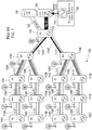
- FIG. 2 is depicts a distributed synchronization between INUs using a radio overhead channel in some embodiments.
- a distributed synchronization is provided between INUs using the radio overhead channel.
- this solution may scale to large IP backhaul access networks while maintaining an IP packet transport scheme over the microwave links.
- a master clock signal 118 is provided by a primary reference clock source 102 to the clock node 202.
- the clock node 202 receives the master clock signal 1 18 and provides the master clock signal 118 to the intelligent node units (INUs).
- INUs intelligent node units
- the clock node 202 and/or the INU 108 may generate a frame that includes a payload for data as well as overhead.
- a root node comprises the clock node 202 and/or the INU 108.
- the overhead may be used to store a synchronization value.
- the synchronization value may be the clock signal, a value associated with the clock signal, and/or a random value (e.g., a pseudorandom binary sequence) that is generated by the clock node 202 and/or the INU 108.
- the synchronization value may be used by one or more other INUs for frequency and phase synchronization. In one example, the synchronization value may be used to align PLL oscillators at remote sites.
- the clock node 202 may provide a synchronization value in a frame that is delivered to INU 108 which may then dedicate seven E1 channels to provide a clock signal or synchronization value to the INU 110a.
- the INU 108 may provide a synchronization value in the frame to INU 110a which may then dedicate three E1 channels 126a to provide a clock signal or the synchronization value to INU 112a.
- operators may transition from the use of E1 channels (i.e., tributaries) in stages and maintain operation of the network rather than being required to convert to an entirely packet-based network.
- INU 108 receives data from the MPLS core node 106 over Ethernet 120.
- the INU 108 when generating the frame, may store the synchronization value in the overhead of the frame while storing the data received from the MPLS core node 106 in the payload of the frame.
- the frame may be provided to one or more other INUs (e.g., INUS 110a-110b).
- the frame may be a traditional frame, a packet, datagram, or any other form of data transmission unit.
- INU 108 may comprise a card (e.g., a NSM) that is configured to receive the clock signal from the clock node 202 and generate the frame.
- the NSM may generate the synchronization value associated with the clock signal.
- the synchronization value may then be stored in the frame (see FIG. 3 ).
- frequency synchronization and/or clock recovery is performed by another NSM.
- Those skilled in the art will appreciate that not all INUs require an NSM.
- only the INU that receives the clock signal (e.., INU 108) and a terminal INU (i.e., an INU that communicates directly with customer equipment rather than to another INU) comprise an NSM.
- the INU 108 with an NSM generates a plurality of frames with a synchronization values. The frames may be received by INU 1 16a with NSM.
- the INU 116a utilizes the synchronization value for frequency synchronization and/or clock recovery.
- the INUs in between INU 108 and INU 116a may not comprise an NSM and may relay the frame and/or synchronization value.
- the INUs in between the INU 108 and the INU 116a will correct for jitter and wander of the frame, contents of the frame, and/or the synchronization value.
- each INU may be upgraded and/or configured to perform jitter attenuation and/or wander attenuation of one or more frames and/or synchronization values.
- many or all INUs may not perform jitter attenuation and my not be upgraded or altered.
- the NSM may comprise an E1/DS1/Clock interface.
- the E1/DS1/Clock interface may provide an electrical translation between the user's external E1 / DS1 or Clock Synchronization Interface formatted signals to TTL level signals processed by the radio system.
- the interface may physically attach to 3x RJ45 connectors (E1/DS 1) and one pair of mini-BNCs (clock interface).
- E1/DS 1 3x RJ45 connectors
- mini-BNCs clock interface
- a line interface of the E1/DS1/Clock interface may be implemented using a Cirrus Logic 61884 octal LIU or similar device. Pulse shapes may conform to relevant G.703 specs for E1, DS1 and Clock interface.
- the NSM may be capable of operating in an E1 and DS1 mode, whereby a line build out and line codes may be software configurable, per tributary.
- the NSM may support Y cables for protection. Support for this function may be obtained by switching out input termination resistors on the offline card.
- frequency synchronization may be required for 2G and 3G FDD base stations, and frequency and phase (relative time) synchronization may be required for 3G and 4G/LTE TDD base stations. Further, in some embodiments, synchronization may be needed for pseudowires used to transport legacy TDM traffic over Ethernet network connections.
- frequency synchronization comprises ensuring master and slave clocks are aligned in frequency.
- Phase synchronization may comprise ensuring that clocks are aligned in phase and to thereby have the same relative time.
- Clocks synchronized in phase may also be synchronized in frequency.
- Universal Mobile Telecommunications System Frequency-Division Duplexing (UMTS-FDD) base stations require synchronization in frequency only, with a synchronization accuracy to 50ppb.
- Base station synchronization may be needed to support optimum handoff between cells, and to ensure frequencies on the air- interfaces have the accuracy and stability needed to minimize channel interference.
- This 50ppb accuracy may be supported over existing TDM network connections via a clock embedded in SDH or PDH frames.
- Systems and methods described herein may provide equivalent accuracy over a packet-switched Ethernet backbone. Examples of FDD cellular technologies include GSM, GPRS, EDGE, CDMA, and WCDMA.
- Various embodiments described herein provide an option for base station synchronization when data services are overlaid on existing TDM networks. Further, various embodiments described herein may provide solutions applicable to IP/Ethernet backhaul over microwave radio.
- UMTS- Time-division duplexing (UMTS-TDD) base stations require both frequency and phase synchronization.
- Base stations may be phase aligned to ensure frames transmitted by neighboring stations are aligned in time (relative time) for channel handover and minimization of cross-channel interference.
- the phase accuracy required may be in the order of 1us to 10us, depending on the system.
- GPS may be required for this level of accuracy.
- TDD technologies include WiMAX-TDD, TD-CDMA and TD-SCDMA. There is no standardized solution for network delivery of real time to the required level of accuracy in the prior art.
- FIG. 3 is a diagram of an exemplary frame 300 in some embodiments.
- an INU constructs a frame that comprises a payload 302, overhead 304 for network management communication and small bit rate Aux channels, and forward error protection (FEC) 306.
- the overhead channels may be a small proportion (e.g., 256kbits) of the payload channel (e.g., 8Mbits upwards to 300Mbits).
- the INU comprises a radio access card configured to construct the frame 300.
- a microwave radio link comprises outdoor units (ODUs) which perform frequency translation to and from microwave radio channels.
- OFDUs outdoor units
- data e.g., voice data
- a synchronization value is stored in the overhead 304.
- the synchronization value may comprise 64kbits.
- the synchronization value may comprise any bit rate.
- when packets are generated all or part of the overhead is unused. By transferring the synchronization value via the overhead, synchronization may be accomplished without reducing valuable payload space.
- the overhead of the frame 300 may comprise a message (e.g., an SSM message) in this channel.
- the SSM message may comprise status or control information.
- the status or control information comprises a message describing the quality of the synchronization value.
- the quality of the clock signal from the master clock and/or synchronization value based on the clock signal from the master clock may be very high. As the number of INUs increase, however, jitter or wander may reduce the quality of the clock signal and/or synchronization value.
- the message in the overhead may be updated accordingly to provide information regarding the quality of the clock signal and/or synchronization value to other INUs.
- a first INU may receive one or more clock signal(s) and/or synchronization value(s) from another INU.
- the first INU may also receive a second clock signal from another source such as a GPS. If, based on the message in the overhead, the first INU determines that the second clock signal may be more accurate, then the first INU may utilize the new clock signal from the GPS. Similarly, the first INU may provide the new clock signal and/or synchronization value associated with the new clock signal to other INUs or customers.
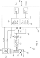
- FIG. 4 is a diagram of a network synchronization module (NSM) 400 in some embodiments.
- the NSM 400 provides connectivity between the E1/DS1 or 2.048/1.544MHz clocks and the INU TDM buses' 64kbit/s Auxiliary channels for the purpose of carrying clock timing information across a network using the overhead channels in the radio section.
- the NSM 400 may provide a rate conversion from 2.048/1.544MHz to 64kHz and reduce or minimize jitter and wander accumulation.
- the NSM 400 comprises an optional programmable clock generator 402, a 3 port RJ 45 connector 404, a sync in port 406, a sync out port 408, quad magnetics 410, a ckt side prot. 412, a line-in unit (LIU) 414, and an FPGA 416.
- the FPGA 416 may comprise a DPLL 420 for providing a synchronization value to an auxiliary channel and a DPLL 418 for providing a synchronization value to a bus.
- the programmable clock generator 402 may provide a master clock signal to the LIU 414 and an AIS_Clk signal to the FPGA 416.
- the clock signal may be received from any clock generator that may or may not be a part of the NSM 400.
- the quad magnetics 410 may be configured to send or receive information via the 3 port RJ-45 connector 404. Further, the quad magnetics 410 may be configured to provide information via the sync out port 408 or receive information via the sync in port 406.
- the ckt side pro 412 is configured to provide information between the quad magnetics 410 and the LIU 414.
- the LIU 414 may provide the information to the FPGA 416.
- the DPLL 418 may receive a synchronization value from a frame.
- the DPLL 420 may attenuate jitter and convert the synchronization value from 64kHz to 2.048/1.544 mHz.
- the DPLL 418 may attenuate jitter and convert the synchronization value from 2.048/1.544 mHz to 64kHz.
- a synchronization value may be received via the sync in port 406 and/or the 3 port RJ-45 connector 404.
- a clock signal and/or synchronization value may be provided by the the sync out port 408 and/or the 3 port RJ-45 connector 404.
- the FPGA/DPLL 416 may provide connectivity between the LIU 414 and the INU TDM backplane bus 422.
- the FPGA/DPLL 416 functions may include clock rate conversion from (in conjunction with a programmable DPLL) to 64 kHz, and TDM bus write / read to Auxiliary channels.
- the FPGA 416 function comprise off- the-shelf devices such as the Xilinx Spartan 3 1000 series FPGA.
- the FPGA 416 may contain a programmable block to select one auxiliary channel on the TDM bus for the purposes of carrying 2.048 or 1.544 MHz clocks. Bit stuffing and de-stuffing may be used on the dedicated backplane timeslot.
- the FPGA 416 and DPLL (418 and/or 420) may provide rate adaptation to convert one or more of the three designated E1 or DS1 inputs or the clock input from the user to the auxiliary channel.
- the FPGA 416 and DPLL (418 and/or 420) may provide rate adaptation to convert one auxiliary channel to 2.048 or 1.544 MHz to be commonly fed to one or more LIU 414 output ports towards the user.
- the FPGA 416 may allow a user input (E1/DS 1 or clock) to be optionally fanned out to all output ports (i.e. not taking timing from the backplane). In this way the NSM 400 may acts to source timing to the backplane and replicate timing elsewhere (e.g., to another INU).
- E1/DS 1 or clock a user input
- the NSM 400 may acts to source timing to the backplane and replicate timing elsewhere (e.g., to another INU).
- the FPGA 416 and DPLL (418 and/or 420) may remove jitter on the auxiliary channel from the TDM bus such that single and multiple radio hops meet system wide (G.823) jitter and wander specifications.
- the FPGA 416 may provide a pseudorandom pattern generator towards the user for those LIU ports carrying E1s or DSIs.
- the pseudorandom pattern generated may be user configurable to include, for example, 2 15 -1 and 2 20 -1.
- the FPGA 416 may carry an AIS (all ones) signal to the user (E1/DS1s) when the timing signal is lost (e.g. radio path down). Further, the FPGA 416 may enable tributary input impedances to change depending on whether the card is operating in protected 'Y' cable mode or not.
- AIS all ones
- FIG. 5 is a diagram of an exemplary field-programmable gate array (FPGA) 416 in some embodiments.
- the FPGA 416 performs the clock conversion function while minimizing jitter and/or wander that accumulates as the clock transitions from NSM 400 to the TDM backplane 522 to radio path and onwards through potentially many radio paths before exiting at another NSM.
- Each hop whether between NSMs via the backplane or between cards via microwave links has the potential to introduce jitter and wander especially where a bit stuffing technique is used to carry signals across clock boundaries.
- the NSM 400 performs jitter attenuation of the 64 kHz auxiliary channel at the NSM backplane interface and potentially other interfaces depending on the performance requirements.
- a radio access card may combine the auxiliary data with other backplane traffic (e.g., IP traffic) prior to transmission through a modem over a microwave radio network.
- the 64 kHz Aux channel may carry a random data pattern (i.e., a synchronization value) across the microwave network, in order, in some embodiments, to convey data at an average rate, but ignoring the actual data itself.
- the average rate of data arriving at the NSM 400 from the TDM backplane 522 may be used to regenerate a smoothed clock multiplied up to the user ports which may be the function of the PLL described herewith.
- the FPGA 416 may comprise mux 502 and loss of signal (LOS) alarm mux 504 which receive information from the LIU 414.
- a source select signal may control the mux 502 and/or the LOS alarm mux 504.
- a clock signal may be provided to the FPGA 416 from the LIU 414.
- a PLL 506 may receive the clock signal via the mux 502.
- the clock signal may be at 1.544 or 2.048 MHz.
- the PLL 506 may downconvert the clock signal from the LIU 414 from 1.544/2.048 MHz to 64 KHz.
- the downconverted signal may be provided to a pseudorandom binary sequence (PRBS) generator 508 which generates a PRBS.
- PRBS pseudorandom binary sequence
- a second clock signal may also be received by the AIS 510.
- a mux 514 may select between the clock signal of the AIS 510 or the PRBS from the PRBS generator 508.
- the mux 514 may be controlled by a signal indicating a loss of signal from the LIU 414 or a failure of the PLL 506 to lock. If there is a loss of signal or failure of the PLL 506 to lock, the mux 514 may select the signal from the AIS 510.
- the Aux Mux 516 receives the output of the mux 514.
- the frame config. RAM 520 may be configured to control mux 518 to control placement of the synchronization value on the TDM backplane 522.
- the frame config. RAM 526 may control mux 524 for retrieving a synchronization value from the TDM backplane 522.
- An Aux demux may receive the synchronization value from the mux 524.
- the Aux demux comprises a jitter attenuator 532, a PRBS monitor 528, and a PRBS lock detector 530.
- the PRBS monitor 528 may receive the synchronization value and the PRBS lock detector 530 may receive a signal from the PRBS monitor 528.
- the jitter attenuator 532 attenuates jitter (if any) of the synchronization value from the mux 524.
- the PLL 534 may upconvert the synchronization value from the jitter attenuator 532 (e.g., from 64 kHz to 1.544/2.048 MHz).
- a mux 538 may select between a 1.544/2.048 MHz reference signal and the signal from the output from the PLL 534.
- the mux 538 may select the 1.544/2.048 MHz signal if the PLL 534 lock fails or the PRBS lock detector 530 indicates a lock fail.
- the AIS 540, the PRBS generator 542, and the mux 546 may receive the output from the mux 538.
- the mux 544 selects between the signal received from the AIS 540 and the PRBS from the PRBS generator 542.
- the mux 544 may be controlled by the lock fail signal from the PRBS lock detector 530 and/or the PLL 534 lock failure signal.
- the output of the mux 544 is provided to the LIU 414.
- the mux 546 is controlled by a master reference loopback to select between a 1.544/2.048 MHz signal and the output of mux 538.
- the output of mux 546 is provided to LIU 414.
- the PLL 506 and/or the PLL 534 may be digital PLLs.
- FIG. 6 is a diagram of a PLL 600 with a jitter attenuator in some embodiments.
- a PLL on the FPGA 416 may be used to change frequencies and/or smooth phase variations of a clock.
- the PLL 600 depicts a model of a PLL whereby the incoming clock frequency may be divided (e.g., by divider 602) down to a common comparison frequency at the input to a phase detector 604.
- the phase detector output may feed a loop filter 608 which drives a VCO 610. This may be an output clock, a sample of which may be fed back to the phase detector 604 to close the loop.
- the dividers 602 and 612 may convert input to output frequencies. For instance, 2.048MHz may be divided by 256 to give a comparison frequency of 8 kHz and the VCO 610 output of 64 kHz may be divided by 8 to match this comparison frequency.
- This is one possible configuration of the NSM input to backplane PLL direction. Similar ratios can be used in the reverse direction.
- Pure jitter attenuation may be achieved by setting the dividers to equal values, and using the divider counters to address FIFO 614 write and read pointers.
- a suitable phase detector for example the commonly known JK flipflop
- the PLL 600 may align the read and write to be maximally apart, thus allowing for system induced phase variation to be absorbed and data to be passed without or with little error.
- loop filter 608 may set the order of the PLL 600.
- a proportional and integral loop filter 608 may be used to give a second order loop with independently settable loop bandwidth and damping factors. These two factors may determine the level of jitter and wander presented at the output and considerable opportunity is available to optimizing these for a given system.
- FIG. 7 shows propagation of a clock signal in ring- or mesh-like networks 700 in some embodiments.
- a PRBS random pattern is transported over the Aux channel.
- Clock quality information or other status information may be stored in the channel so as to allow switching to alternative clock sources in the case of failure.
- the network 700 comprises of a ring backbone with four routers 702, 704, 706, and 708 and spurs with base stations 710, 712, 714, 716, 718, 720, 722, 724, 726, 728, and 730. All nodes may be interconnected by radio. There may be two GPS clock sources 732 and 734. In some embodiments, all nodes receive a clock from a Master GPS as shown below by arrows.
- a switch may select different input as a clock source. Selection may be done based on SSM messages (e.g., indicating clock quality information or other status information), which indicates quality of a clock received at each input.
- SSM messages e.g., indicating clock quality information or other status information
- the following diagram depicts clock propagation when link between two routers failed (i.e., at the x between routers 702 and 704).
- the Aux channel may carry messages (e.g., SSM messages) in addition to a synchronization value.
- SSM e.g., SSM messages
- the SSM may be carried in the E1/DS1 overhead.
- the NSM may also be able to carry the SSM messages through 64 Kbps auxiliary channel. SSM messages may be extracted at NSM inputs (e.g., both E1/DS1 and 64 Kbps) and inserted at outputs.
- the NSM architecture comprises a 64 Kbps auxiliary channel which, when used to carry a synchronization value, may provide a way to carry clock traceability information (SSM information).
- SSM information clock traceability information
- Frame format SF (D4) or ESF may be configured for DS1 inputs. This configuration may be on per port basis. Further, Sa-bit used for SSM information may be selected for E1 inputs. This configuration may also be on per port basis.
- the NSM card may extract SSM information from E1/DS1 inputs (when available) and map it into 64 Kbps auxiliary channel.
- E1/DS1 input does not have SSM information
- the NSM card may include a SSM indicating "traceability unknown” in the 64 Kbps channel.
- a SSM indicating "equipment internal clock” may be inserted into 64 Kbps channel.
- the NSM when the NSM recovers a clock from a 64 Kbps channel, the NSM may use SSM information from the 64 Kbps channel and include the SSM information in the generated E1 or DS1 output.
- an SSM indicating "equipment internal clock" may be used.
- An E1/DS1 port may be configured as an independent input and output or as a "pair.”
- the "pair" mode may indicate that the port provides bi-directional communication with another device and that direction of clock propagation could reverse depending on overall network status.
- the SSM indicating "Do not use for synchronization" may be used for this output. This may limit or prevent clock loops. In some embodiments, all other ports output may include actual SSM information.
- FIG. 8 is an exemplary NSM 800 configured to retrieve and input SSM in some embodiments.
- FIG. 8 comprises components of FIG. 5 as well a deframer 802 configured to retrieve SSM from the TDM bus over the Aux. channel.
- the SSM may be provided over E1/DS1 #1-3 by framers 804.
- framers 804 may be a part of the LIU 414 or the FPGA 416.
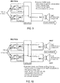
- FIG. 9 depicts NSM redundancy in some embodiments.
- two NSMs NSM 1 and 2 may be operably coupled to an RAC. If one of the NSMs fails, the other may provide a synchronization value to the RAC. Further, if PRC is inaccurate or there is a loss of signal, either NSM 1 or NSM 2 may provide a synchronization value via E1/DS1.
- the two NSMs share inputs from the PRC and the E1/DS1. As a result, redundancy is provided if one of the two NSMs fail or if only part of one NSM fails (e.g., PRC input to the NSM 1 failed but the PRC input may be provided to the RAC by NSM 2).
- the PRC signal may be received only by the NSM 1 and the E1/DS1 clock signal may be received by NSM 2. If the PRC signal fails or is otherwise found inaccurate, the NSM 2 may provide a synchronization value to the RAC based on the E1/DS1 clock signal.
- a single NSM may support both receiving a PRC signal in at least one port and an E1/DS1 clock signal in at least one other port. If a port or a PRC signal fails or is otherwise inaccurate, the NSM may provide the synchronization value associated with the E1/DS1 clock signal to the RAC.
- FIG. 10 depicts NSM and RAC redundancy in some embodiments.
- two NSMs, NSM 1 and 2 may be operably coupled to two RACs (i.e., RAC 1 and RAC 2).
- this circuit provides the advantages of the circuit depicted in FIG. 9 but may also provide redundancy if one of the RACs fail.
- the components depicted in FIG. 10 may be used in conjunction with clocks received from a ring network.
- the two NSMs share inputs from the PRC and the E1/DS1. As a result, redundancy is provided if one of the two NSMs fail or if only part of one NSM fails (e.g., PRC input to the NSM 1 failed but the PRC input may be provided to the RAC by NSM 2).
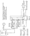
- FIG. 11 depicts NSM redundancy in a ring network in some embodiments.
- PRC 1 may be supported by a clock (sub-master PRC2) at a different point in the network.
- FIG. 11 illustrates the node supporting the remote PRC2 clock.
- Clock sourcing for PRC1 or PRC2 at the local eNode B may be an eNode B function.
- NSM clocking may be transported in AUX1 and AUX2.
- PRC 1 and 2 are not provided and the NSM synchronizes the eNode B.
- the above-described functions and components can be comprised of instructions that are stored on a storage medium such as a computer readable medium.
- the instructions can be retrieved and executed by a processor.
- Some examples of instructions are software, program code, and firmware.
- Some examples of storage medium are memory devices, tape, disks, integrated circuits, and servers.
- the instructions are operational when executed by the processor to direct the processor to operate in accord with embodiments of the present invention. Those skilled in the art are familiar with instructions, processor(s), and storage medium.
Landscapes
- Engineering & Computer Science (AREA)
- Computer Networks & Wireless Communication (AREA)
- Signal Processing (AREA)
- Synchronisation In Digital Transmission Systems (AREA)
- Mobile Radio Communication Systems (AREA)
Claims (20)
- System, Folgendes beinhaltend:eine Uhr (102), welche konfiguriert ist, um ein erstes Uhrsignal (118) zu erzeugen;einen Wurzelknoten (202), welcher konfiguriert ist, um das erste Uhrsignal zu empfangen, um einen ersten Rahmen zu erzeugen, welcher erste Nutzdaten und erste Zusatzdaten enthält, und um einen zweiten Rahmen zu erzeugen, welcher zweite Nutzdaten und zweite Zusatzdaten enthält, wobei die ersten Zusatzdaten einen Synchronisationswert basierend auf dem ersten Uhrsignal beinhalten, und die zweiten Zusatzdaten ebenfalls den Synchronisationswert beinhalten;ein Funkkanalnetzwerk in Kommunikation mit dem Wurzelknoten zum Übertragen des ersten Rahmens und des zweiten Rahmens;einen ersten untergeordneten Knoten (INU 108), welcher einen ersten Phasenregelkreis enthält und konfiguriert ist, um den ersten Rahmen zu empfangen und um Taktrückgewinnung einschließlich einer Frequenzsynchronisation unter Verwendung des Synchronisationswertes und des ersten Phasenregelkreises zu bewerkstelligen;einen zweiten untergeordneten Knoten (INU 116a), welcher einen zweiten Phasenregelkreis enthält und konfiguriert ist, um den zweiten Rahmen zu empfangen und um Taktrückgewinnung einschließlich einer Frequenzsynchronisation unter Verwendung des Synchronisationswertes und des zweiten Phasenregelkreises zu bewerkstelligen; und gekennzeichnet durcheinen untergeordneten Zwischenknoten (NSM 400), welcher einen dritten Phasenregelkreis enthält und konfiguriert ist, um den ersten Rahmen vom Wurzelknoten zu empfangen, bevor der erste untergeordnete Knoten den ersten Rahmen empfängt, um eine mittlere Datenrate unter Verwendung des Synchronisationswertes aus dem ersten Rahmen zu bestimmen, um die mittlere Datenrate zu verwenden, um ein zweites Uhrsignal zu glätten, welches durch den dritten Phasenregelkreis verwendet wird, und um den dritten Phasenregelkreis mit dem geglätteten zweiten Uhrsignal zu verwenden, um Jitter des ersten Rahmens, welcher den Synchronisationswert enthält, abzuschwächen.
- System nach Anspruch 1, bei welchem das Funkkanalnetzwerk ein Mikrowellen-Netzwerk enthält.
- System nach Anspruch 1, bei welchem der erste untergeordnete Knoten konfiguriert ist, um Jitter des ersten Rahmens abzuschwächen.
- System nach Anspruch 1, bei welchem der Wurzelknoten konfiguriert ist, um eine erste Serie von Rahmen für den ersten untergeordneten Knoten zu erzeugen, und um eine erste Serie von Synchronisationswerten für die erste Serie von Rahmen zu erzeugen.
- System nach Anspruch 4, bei welchem der Wurzelknoten konfiguriert ist, um eine zweite Serie von Rahmen für den zweiten untergeordneten Knoten zu erzeugen, und um die erste Serie von Synchronisationswerten für die zweite Serie von Rahmen zu verwenden.
- System nach Anspruch 1, bei welchem der Synchronisationswert eine pseudozufällige Sequenz enthält.
- System nach Anspruch 4, bei welchem ein jeder der ersten Serie von Synchronisationswerten derselbe Wert ist.
- System nach Anspruch 1, zudem beinhaltend einen Knoten mit Multiprotocol Label Switching (MPLS), welcher konfiguriert ist, um dem Wurzelknoten Daten bereitzustellen.
- System nach Anspruch 1, bei welchem die Zusatzdaten zudem eine Uhrzeit-Qualitätsmeldung beinhalten.
- System nach Anspruch 9, bei welchem der erste untergeordnete Knoten konfiguriert ist, um zwischen dem Synchronisationswert und einem zweiten Urzeitsignal zumindest teilweise basierend auf der Uhrzeit-Qualitätsmeldung zu wählen.
- Verfahren, folgende Schritte beinhaltend:Erzeugen eines ersten Urzeitsignals;Erzeugen, durch einen Wurzelknoten, eines ersten Rahmens, welcher erste Nutzdaten und erste Zusatzdaten enthält, wobei die ersten Zusatzdaten einen Synchronisationswert basierend auf dem ersten Urzeitsignal beinhalten;Erzeugen, durch den Wurzelknoten, eines zweiten Rahmens, welcher zweite Nutzdaten und zweite Zusatzdaten enthält, wobei die zweiten Zusatzdaten ebenfalls den Synchronisationswert beinhalten;Übertragen des ersten Rahmens und des zweiten Rahmens über ein Funkkanalnetzwerk;gekennzeichnet durch:Empfangen des ersten Rahmens vom Wurzelknoten durch einen untergeordneten Zwischenknoten, bevor ein erster untergeordneter Knoten den ersten Rahmen empfängt;Bestimmen einer mittleren Datenrate unter Verwendung des Synchronisationswertes aus dem ersten Rahmen;Glätten, unter Verwendung der mittleren Datenrate, eines zweiten Urzeitsignals, welches durch einen dritten Phasenregelkreis des untergeordneten Zwischenknotens verwendet wird;Abschwächen, durch den dritten Phasenregelkreis mit dem geglätteten zweiten Uhrzeitsignal, von Jitter des ersten Rahmens, welcher den Synchronisationswert enthält;Empfangen des ersten Rahmens durch den ersten untergeordneten Knoten;Bewerkstelligen, durch den ersten untergeordneten Knoten, von Taktrückgewinnung einschließlich einer Frequenzsynchronisation unter Verwendung des Synchronisationswertes und eines ersten Phasenregelkreises;Empfangen des zweiten Rahmens durch einen zweiten untergeordneten Knoten; undBewerkstelligen, durch den zweiten untergeordneten Knoten, von Taktrückgewinnung einschließlich einer Frequenzsynchronisation unter Verwendung des Synchronisationswertes und eines zweiten Phasenregelkreises.
- Verfahren nach Anspruch 11, bei welchem das Funkkanalnetzwerk ein Mikrowellen-Netzwerk enthält.
- Verfahren nach Anspruch 11, zudem beinhaltend das Abschwächen von Jitter des ersten Rahmens durch den ersten untergeordneten Knoten.
- Verfahren nach Anspruch 11, zudem beinhaltend das Erzeugen einer ersten Serie von Rahmen für den ersten untergeordneten Knoten durch den Wurzelknoten und das Erzeugen einer ersten Serie von Synchronisationswerten für die erste Serie von Rahmen.
- Verfahren nach Anspruch 14, zudem beinhaltend das Erzeugen einer zweiten Serie von Rahmen für den zweiten untergeordneten Knoten durch den Wurzelknoten und das Verwenden der ersten Serie von Synchronisationswerten für die zweite Serie von Rahmen.
- Verfahren nach Anspruch 11, bei welchem der Synchronisationswert eine pseudozufällige Sequenz enthält.
- Verfahren nach Anspruch 14, bei welchem ein jeder der ersten Serie von Synchronisationswerten derselbe Wert ist.
- Verfahren nach Anspruch 11, zudem beinhaltend das Bereitstellen von Daten von einem Knoten mit Multiprotocol Label Switching (MPLS) an den Wurzelknoten.
- Verfahren nach Anspruch 11, bei welchem die Zusatzdaten zudem eine Uhrzeit-Qualitätsmeldung beinhalten.
- Verfahren nach Anspruch 19, zudem beinhaltend das Auswählen zwischen dem Synchronisationswert und einem zweiten Urzeitsignal, welches zumindest teilweise auf der Uhrzeit-Qualitätsmeldung basiert.
Priority Applications (1)
| Application Number | Priority Date | Filing Date | Title |
|---|---|---|---|
| SI201031948T SI2467976T1 (sl) | 2009-08-21 | 2010-08-23 | Sinhoronizacijska porazdelitev v mikrovalovnih povratnih mrežah |
Applications Claiming Priority (2)
| Application Number | Priority Date | Filing Date | Title |
|---|---|---|---|
| US23603209P | 2009-08-21 | 2009-08-21 | |
| PCT/US2010/046393 WO2011022735A1 (en) | 2009-08-21 | 2010-08-23 | Synchronization distribution in microwave backhaul networks |
Publications (3)
| Publication Number | Publication Date |
|---|---|
| EP2467976A1 EP2467976A1 (de) | 2012-06-27 |
| EP2467976A4 EP2467976A4 (de) | 2014-06-11 |
| EP2467976B1 true EP2467976B1 (de) | 2019-10-09 |
Family
ID=43607367
Family Applications (1)
| Application Number | Title | Priority Date | Filing Date |
|---|---|---|---|
| EP10810727.7A Active EP2467976B1 (de) | 2009-08-21 | 2010-08-23 | Synchronisationsverteilung in mikrowellen-backhaul-netzwerken |
Country Status (7)
| Country | Link |
|---|---|
| US (3) | US8565361B2 (de) |
| EP (1) | EP2467976B1 (de) |
| CN (1) | CN102598589A (de) |
| MY (1) | MY154335A (de) |
| SG (1) | SG178498A1 (de) |
| SI (1) | SI2467976T1 (de) |
| WO (1) | WO2011022735A1 (de) |
Families Citing this family (20)
| Publication number | Priority date | Publication date | Assignee | Title |
|---|---|---|---|---|
| US8428045B2 (en) * | 2010-03-16 | 2013-04-23 | Harman International Industries, Incorporated | Media clock recovery |
| US8976778B2 (en) * | 2010-04-21 | 2015-03-10 | Lsi Corporation | Time synchronization using packet-layer and physical-layer protocols |
| US8730101B2 (en) * | 2010-05-13 | 2014-05-20 | Qualcomm Incorporated | High sensitivity satellite positioning system receiver |
| US9568609B2 (en) | 2010-05-13 | 2017-02-14 | Qualcomm Incorporated | High sensitivity satellite positioning system receiver |
| EP2759081B1 (de) * | 2011-09-22 | 2016-11-16 | Aviat Networks, Inc. | Systeme und verfahren zur synchronisierung von taktsignalen |
| US10425117B2 (en) | 2011-11-30 | 2019-09-24 | Maxlinear Asia Singapore PTE LTD | Split microwave backhaul architecture with smart outdoor unit |
| US9621330B2 (en) | 2011-11-30 | 2017-04-11 | Maxlinear Asia Singapore Private Limited | Split microwave backhaul transceiver architecture with coaxial interconnect |
| US9380645B2 (en) | 2011-11-30 | 2016-06-28 | Broadcom Corporation | Communication pathway supporting an advanced split microwave backhaul architecture |
| US9794807B2 (en) | 2011-11-30 | 2017-10-17 | Maxlinear Asia Singapore PTE LTD | Management of backhaul nodes in a microwave backhaul |
| IL217232A0 (en) * | 2011-12-27 | 2012-03-29 | Eci Telecom Ltd | Technique for monitoring and management of data networks |
| US9825724B2 (en) | 2013-01-08 | 2017-11-21 | Aviat U.S., Inc. | Systems and methods for transporting a clock signal over a network |
| EP2959600B1 (de) * | 2013-02-22 | 2020-08-26 | Telefonaktiebolaget LM Ericsson (publ) | Zeitsynchroner einsteckbarer sender/empfänger |
| US9386552B2 (en) * | 2013-09-30 | 2016-07-05 | Honeywell International Inc. | Wireless sensor time synchronization |
| KR101596756B1 (ko) * | 2014-11-03 | 2016-03-07 | 현대자동차주식회사 | 리던던트 그랜드마스터를 이용한 차량 내 네트워크 시간 동기화 제공 방법 및 장치 |
| CN108604979B (zh) * | 2016-02-02 | 2021-05-18 | 马维尔亚洲私人有限公司 | 用于网络同步的方法和装置 |
| US9742549B1 (en) * | 2016-09-29 | 2017-08-22 | Analog Devices Global | Apparatus and methods for asynchronous clock mapping |
| US10158442B1 (en) * | 2016-12-13 | 2018-12-18 | Amazon Technologies, Inc. | Reliable precision time architecture |
| US10164759B1 (en) | 2016-12-13 | 2018-12-25 | Amazon Technologies, Inc. | Distributed precision time architecture |
| SE1900029A1 (en) | 2019-02-15 | 2020-08-16 | Telefonaktiebolaget L M Ericsson Publ | IAB downlink timing |
| CN114650113B (zh) * | 2020-12-18 | 2024-07-16 | 华为技术有限公司 | 选择时钟源的方法及装置 |
Citations (1)
| Publication number | Priority date | Publication date | Assignee | Title |
|---|---|---|---|---|
| US20080298398A1 (en) * | 2007-06-04 | 2008-12-04 | John C Eidson | Transparent Spider |
Family Cites Families (13)
| Publication number | Priority date | Publication date | Assignee | Title |
|---|---|---|---|---|
| US5182761A (en) * | 1991-01-31 | 1993-01-26 | Motorola, Inc. | Data transmission system receiver having phase-independent bandwidth control |
| US5761255A (en) * | 1995-11-30 | 1998-06-02 | The Boeing Company | Edge-synchronized clock recovery unit |
| US6549242B1 (en) * | 1997-04-04 | 2003-04-15 | Harris Corporation | Combining adjacent TV channels for transmission by a common antenna |
| US8274892B2 (en) * | 2001-10-09 | 2012-09-25 | Infinera Corporation | Universal digital framer architecture for transport of client signals of any client payload and format type |
| GB0205142D0 (en) * | 2002-03-05 | 2002-04-17 | Nokia Corp | Synchronisation in communication systems |
| ITSV20020018A1 (it) * | 2002-05-03 | 2003-11-03 | Alstom Transp Spa | Dispositivo di elaborazione o comando operante in sicurezza intrinseca |
| US7397314B2 (en) * | 2002-09-11 | 2008-07-08 | Hewlett-Packard Development Company, L.P. | Redundant clock source |
| US7495516B2 (en) * | 2003-04-02 | 2009-02-24 | Christopher Julian Travis | Method of establishing an oscillator clock signal |
| US7372853B2 (en) * | 2003-06-25 | 2008-05-13 | Fujitsu Limited | Method and system for multicasting data packets in an MPLS network |
| US7239626B2 (en) * | 2004-06-30 | 2007-07-03 | Sharp Laboratories Of America, Inc. | System clock synchronization in an ad hoc and infrastructure wireless networks |
| EP2822284B1 (de) * | 2007-10-04 | 2015-12-30 | Microchip Technology Germany GmbH | System für Videoübertragung in Echtzeit |
| US8958441B2 (en) * | 2008-06-05 | 2015-02-17 | Qualcomm Incorporated | System and method of an in-band modem for data communications over digital wireless communication networks |
| KR100994128B1 (ko) * | 2008-09-23 | 2010-11-15 | 한국전자통신연구원 | 고정밀 네트워크 동기를 위한 타임 스탬핑 방법 및 장치 |
-
2010
- 2010-08-23 SG SG2012011458A patent/SG178498A1/en unknown
- 2010-08-23 WO PCT/US2010/046393 patent/WO2011022735A1/en not_active Ceased
- 2010-08-23 SI SI201031948T patent/SI2467976T1/sl unknown
- 2010-08-23 EP EP10810727.7A patent/EP2467976B1/de active Active
- 2010-08-23 CN CN2010800478973A patent/CN102598589A/zh active Pending
- 2010-08-23 MY MYPI2012000739A patent/MY154335A/en unknown
- 2010-08-23 US US12/861,786 patent/US8565361B2/en active Active
-
2013
- 2013-10-22 US US14/060,503 patent/US8983015B2/en active Active
-
2015
- 2015-02-03 US US14/613,264 patent/US9609610B2/en active Active
Patent Citations (1)
| Publication number | Priority date | Publication date | Assignee | Title |
|---|---|---|---|---|
| US20080298398A1 (en) * | 2007-06-04 | 2008-12-04 | John C Eidson | Transparent Spider |
Also Published As
| Publication number | Publication date |
|---|---|
| WO2011022735A1 (en) | 2011-02-24 |
| MY154335A (en) | 2015-05-29 |
| SI2467976T1 (sl) | 2019-12-31 |
| US9609610B2 (en) | 2017-03-28 |
| US20140086375A1 (en) | 2014-03-27 |
| EP2467976A1 (de) | 2012-06-27 |
| US8565361B2 (en) | 2013-10-22 |
| US20150156741A1 (en) | 2015-06-04 |
| US8983015B2 (en) | 2015-03-17 |
| CN102598589A (zh) | 2012-07-18 |
| SG178498A1 (en) | 2012-04-27 |
| US20110080985A1 (en) | 2011-04-07 |
| EP2467976A4 (de) | 2014-06-11 |
Similar Documents
| Publication | Publication Date | Title |
|---|---|---|
| EP2467976B1 (de) | Synchronisationsverteilung in mikrowellen-backhaul-netzwerken | |
| US10637482B2 (en) | Time slotted bus system for multiple coupled digital phase-locked loops | |
| US7535931B1 (en) | Two-way timing protocol | |
| US8693506B2 (en) | Transparent clock adaptor for a network device | |
| CN101534185B (zh) | 时间同步装置、方法和系统 | |
| EP2352250A1 (de) | Zeitsynchronisationsverfahren und -vorrichtung | |
| WO2010047968A2 (en) | Synchronization transport over passive optical networks | |
| CN102237941A (zh) | 时间同步系统及方法 | |
| TW202211631A (zh) | 藉由重置多模數反饋分頻器之無中斷切換 | |
| US8194704B2 (en) | Network equipment | |
| US7145920B2 (en) | SDH transmission apparatus and frame timing re-clocking method for SDH transmission apparatus | |
| EP2564530B1 (de) | Datenübertragung mit multiplexing und demultiplexing von eingebetteten tacksignalen | |
| EP2837117B1 (de) | Taktumschaltungsalgorithmus auf der basis von bevorzugten taktquellen | |
| US9893826B2 (en) | Method for retaining clock traceability over an asynchronous interface | |
| Magee | Synchronization in next-generation mobile backhaul networks | |
| Rodrigues | IEEE-1588 and synchronous Ethernet in telecom | |
| US7551640B1 (en) | Method and apparatus for errorless frame timing adjustment | |
| US8184665B2 (en) | Network device | |
| US7155191B2 (en) | Method and arrangement for reducing phase jumps when switching between synchronization sources | |
| Ouellette et al. | Simulations of a chain of telecom boundary clocks combined with synchronous ethernet for phase/time transfer | |
| Ilišević et al. | Synchronization in mobile backhaul using hybrid microwave links | |
| Manjunath et al. | Synchronization of GSM TDM network through microwave media and its impact on GSM KPI's | |
| Manjunath et al. | An experimental evaluation of impact of synchronization on GSM network performance | |
| Kordnooria et al. | Time synchronization and IEEE 1588v2 solutions | |
| Manjunath et al. | Evaluation of BSC clock frequency drifts on HOSR:—A practical perspective |
Legal Events
| Date | Code | Title | Description |
|---|---|---|---|
| PUAI | Public reference made under article 153(3) epc to a published international application that has entered the european phase |
Free format text: ORIGINAL CODE: 0009012 |
|
| 17P | Request for examination filed |
Effective date: 20120321 |
|
| AK | Designated contracting states |
Kind code of ref document: A1 Designated state(s): AL AT BE BG CH CY CZ DE DK EE ES FI FR GB GR HR HU IE IS IT LI LT LU LV MC MK MT NL NO PL PT RO SE SI SK SM TR |
|
| DAX | Request for extension of the european patent (deleted) | ||
| A4 | Supplementary search report drawn up and despatched |
Effective date: 20140514 |
|
| RIC1 | Information provided on ipc code assigned before grant |
Ipc: H03L 7/18 20060101ALI20140508BHEP Ipc: H04J 3/06 20060101AFI20140508BHEP |
|
| 17Q | First examination report despatched |
Effective date: 20160429 |
|
| STAA | Information on the status of an ep patent application or granted ep patent |
Free format text: STATUS: EXAMINATION IS IN PROGRESS |
|
| GRAP | Despatch of communication of intention to grant a patent |
Free format text: ORIGINAL CODE: EPIDOSNIGR1 |
|
| STAA | Information on the status of an ep patent application or granted ep patent |
Free format text: STATUS: GRANT OF PATENT IS INTENDED |
|
| INTG | Intention to grant announced |
Effective date: 20190322 |
|
| GRAS | Grant fee paid |
Free format text: ORIGINAL CODE: EPIDOSNIGR3 |
|
| GRAA | (expected) grant |
Free format text: ORIGINAL CODE: 0009210 |
|
| STAA | Information on the status of an ep patent application or granted ep patent |
Free format text: STATUS: THE PATENT HAS BEEN GRANTED |
|
| AK | Designated contracting states |
Kind code of ref document: B1 Designated state(s): AL AT BE BG CH CY CZ DE DK EE ES FI FR GB GR HR HU IE IS IT LI LT LU LV MC MK MT NL NO PL PT RO SE SI SK SM TR |
|
| REG | Reference to a national code |
Ref country code: GB Ref legal event code: FG4D |
|
| REG | Reference to a national code |
Ref country code: CH Ref legal event code: EP |
|
| REG | Reference to a national code |
Ref country code: IE Ref legal event code: FG4D |
|
| REG | Reference to a national code |
Ref country code: DE Ref legal event code: R096 Ref document number: 602010061455 Country of ref document: DE |
|
| REG | Reference to a national code |
Ref country code: AT Ref legal event code: REF Ref document number: 1190047 Country of ref document: AT Kind code of ref document: T Effective date: 20191115 |
|
| REG | Reference to a national code |
Ref country code: NL Ref legal event code: MP Effective date: 20191009 |
|
| REG | Reference to a national code |
Ref country code: LT Ref legal event code: MG4D |
|
| REG | Reference to a national code |
Ref country code: AT Ref legal event code: MK05 Ref document number: 1190047 Country of ref document: AT Kind code of ref document: T Effective date: 20191009 |
|
| PG25 | Lapsed in a contracting state [announced via postgrant information from national office to epo] |
Ref country code: NL Free format text: LAPSE BECAUSE OF FAILURE TO SUBMIT A TRANSLATION OF THE DESCRIPTION OR TO PAY THE FEE WITHIN THE PRESCRIBED TIME-LIMIT Effective date: 20191009 Ref country code: AT Free format text: LAPSE BECAUSE OF FAILURE TO SUBMIT A TRANSLATION OF THE DESCRIPTION OR TO PAY THE FEE WITHIN THE PRESCRIBED TIME-LIMIT Effective date: 20191009 Ref country code: LV Free format text: LAPSE BECAUSE OF FAILURE TO SUBMIT A TRANSLATION OF THE DESCRIPTION OR TO PAY THE FEE WITHIN THE PRESCRIBED TIME-LIMIT Effective date: 20191009 Ref country code: SE Free format text: LAPSE BECAUSE OF FAILURE TO SUBMIT A TRANSLATION OF THE DESCRIPTION OR TO PAY THE FEE WITHIN THE PRESCRIBED TIME-LIMIT Effective date: 20191009 Ref country code: BG Free format text: LAPSE BECAUSE OF FAILURE TO SUBMIT A TRANSLATION OF THE DESCRIPTION OR TO PAY THE FEE WITHIN THE PRESCRIBED TIME-LIMIT Effective date: 20200109 Ref country code: FI Free format text: LAPSE BECAUSE OF FAILURE TO SUBMIT A TRANSLATION OF THE DESCRIPTION OR TO PAY THE FEE WITHIN THE PRESCRIBED TIME-LIMIT Effective date: 20191009 Ref country code: GR Free format text: LAPSE BECAUSE OF FAILURE TO SUBMIT A TRANSLATION OF THE DESCRIPTION OR TO PAY THE FEE WITHIN THE PRESCRIBED TIME-LIMIT Effective date: 20200110 Ref country code: PT Free format text: LAPSE BECAUSE OF FAILURE TO SUBMIT A TRANSLATION OF THE DESCRIPTION OR TO PAY THE FEE WITHIN THE PRESCRIBED TIME-LIMIT Effective date: 20200210 Ref country code: ES Free format text: LAPSE BECAUSE OF FAILURE TO SUBMIT A TRANSLATION OF THE DESCRIPTION OR TO PAY THE FEE WITHIN THE PRESCRIBED TIME-LIMIT Effective date: 20191009 Ref country code: NO Free format text: LAPSE BECAUSE OF FAILURE TO SUBMIT A TRANSLATION OF THE DESCRIPTION OR TO PAY THE FEE WITHIN THE PRESCRIBED TIME-LIMIT Effective date: 20200109 Ref country code: LT Free format text: LAPSE BECAUSE OF FAILURE TO SUBMIT A TRANSLATION OF THE DESCRIPTION OR TO PAY THE FEE WITHIN THE PRESCRIBED TIME-LIMIT Effective date: 20191009 Ref country code: PL Free format text: LAPSE BECAUSE OF FAILURE TO SUBMIT A TRANSLATION OF THE DESCRIPTION OR TO PAY THE FEE WITHIN THE PRESCRIBED TIME-LIMIT Effective date: 20191009 |
|
| PG25 | Lapsed in a contracting state [announced via postgrant information from national office to epo] |
Ref country code: HR Free format text: LAPSE BECAUSE OF FAILURE TO SUBMIT A TRANSLATION OF THE DESCRIPTION OR TO PAY THE FEE WITHIN THE PRESCRIBED TIME-LIMIT Effective date: 20191009 Ref country code: IS Free format text: LAPSE BECAUSE OF FAILURE TO SUBMIT A TRANSLATION OF THE DESCRIPTION OR TO PAY THE FEE WITHIN THE PRESCRIBED TIME-LIMIT Effective date: 20200224 |
|
| PG25 | Lapsed in a contracting state [announced via postgrant information from national office to epo] |
Ref country code: AL Free format text: LAPSE BECAUSE OF FAILURE TO SUBMIT A TRANSLATION OF THE DESCRIPTION OR TO PAY THE FEE WITHIN THE PRESCRIBED TIME-LIMIT Effective date: 20191009 |
|
| REG | Reference to a national code |
Ref country code: DE Ref legal event code: R097 Ref document number: 602010061455 Country of ref document: DE |
|
| PG2D | Information on lapse in contracting state deleted |
Ref country code: IS |
|
| PG25 | Lapsed in a contracting state [announced via postgrant information from national office to epo] |
Ref country code: CZ Free format text: LAPSE BECAUSE OF FAILURE TO SUBMIT A TRANSLATION OF THE DESCRIPTION OR TO PAY THE FEE WITHIN THE PRESCRIBED TIME-LIMIT Effective date: 20191009 Ref country code: RO Free format text: LAPSE BECAUSE OF FAILURE TO SUBMIT A TRANSLATION OF THE DESCRIPTION OR TO PAY THE FEE WITHIN THE PRESCRIBED TIME-LIMIT Effective date: 20191009 Ref country code: DK Free format text: LAPSE BECAUSE OF FAILURE TO SUBMIT A TRANSLATION OF THE DESCRIPTION OR TO PAY THE FEE WITHIN THE PRESCRIBED TIME-LIMIT Effective date: 20191009 Ref country code: EE Free format text: LAPSE BECAUSE OF FAILURE TO SUBMIT A TRANSLATION OF THE DESCRIPTION OR TO PAY THE FEE WITHIN THE PRESCRIBED TIME-LIMIT Effective date: 20191009 Ref country code: IS Free format text: LAPSE BECAUSE OF FAILURE TO SUBMIT A TRANSLATION OF THE DESCRIPTION OR TO PAY THE FEE WITHIN THE PRESCRIBED TIME-LIMIT Effective date: 20200209 |
|
| PLBE | No opposition filed within time limit |
Free format text: ORIGINAL CODE: 0009261 |
|
| STAA | Information on the status of an ep patent application or granted ep patent |
Free format text: STATUS: NO OPPOSITION FILED WITHIN TIME LIMIT |
|
| PG25 | Lapsed in a contracting state [announced via postgrant information from national office to epo] |
Ref country code: SK Free format text: LAPSE BECAUSE OF FAILURE TO SUBMIT A TRANSLATION OF THE DESCRIPTION OR TO PAY THE FEE WITHIN THE PRESCRIBED TIME-LIMIT Effective date: 20191009 Ref country code: SM Free format text: LAPSE BECAUSE OF FAILURE TO SUBMIT A TRANSLATION OF THE DESCRIPTION OR TO PAY THE FEE WITHIN THE PRESCRIBED TIME-LIMIT Effective date: 20191009 |
|
| 26N | No opposition filed |
Effective date: 20200710 |
|
| PG25 | Lapsed in a contracting state [announced via postgrant information from national office to epo] |
Ref country code: MC Free format text: LAPSE BECAUSE OF FAILURE TO SUBMIT A TRANSLATION OF THE DESCRIPTION OR TO PAY THE FEE WITHIN THE PRESCRIBED TIME-LIMIT Effective date: 20191009 |
|
| REG | Reference to a national code |
Ref country code: CH Ref legal event code: PL |
|
| PG25 | Lapsed in a contracting state [announced via postgrant information from national office to epo] |
Ref country code: LU Free format text: LAPSE BECAUSE OF NON-PAYMENT OF DUE FEES Effective date: 20200823 Ref country code: LI Free format text: LAPSE BECAUSE OF NON-PAYMENT OF DUE FEES Effective date: 20200831 Ref country code: CH Free format text: LAPSE BECAUSE OF NON-PAYMENT OF DUE FEES Effective date: 20200831 |
|
| REG | Reference to a national code |
Ref country code: BE Ref legal event code: MM Effective date: 20200831 |
|
| PG25 | Lapsed in a contracting state [announced via postgrant information from national office to epo] |
Ref country code: BE Free format text: LAPSE BECAUSE OF NON-PAYMENT OF DUE FEES Effective date: 20200831 Ref country code: IE Free format text: LAPSE BECAUSE OF NON-PAYMENT OF DUE FEES Effective date: 20200823 |
|
| PG25 | Lapsed in a contracting state [announced via postgrant information from national office to epo] |
Ref country code: TR Free format text: LAPSE BECAUSE OF FAILURE TO SUBMIT A TRANSLATION OF THE DESCRIPTION OR TO PAY THE FEE WITHIN THE PRESCRIBED TIME-LIMIT Effective date: 20191009 Ref country code: MT Free format text: LAPSE BECAUSE OF FAILURE TO SUBMIT A TRANSLATION OF THE DESCRIPTION OR TO PAY THE FEE WITHIN THE PRESCRIBED TIME-LIMIT Effective date: 20191009 Ref country code: CY Free format text: LAPSE BECAUSE OF FAILURE TO SUBMIT A TRANSLATION OF THE DESCRIPTION OR TO PAY THE FEE WITHIN THE PRESCRIBED TIME-LIMIT Effective date: 20191009 |
|
| PG25 | Lapsed in a contracting state [announced via postgrant information from national office to epo] |
Ref country code: MK Free format text: LAPSE BECAUSE OF FAILURE TO SUBMIT A TRANSLATION OF THE DESCRIPTION OR TO PAY THE FEE WITHIN THE PRESCRIBED TIME-LIMIT Effective date: 20191009 |
|
| PGFP | Annual fee paid to national office [announced via postgrant information from national office to epo] |
Ref country code: SI Payment date: 20250710 Year of fee payment: 16 |
|
| PGFP | Annual fee paid to national office [announced via postgrant information from national office to epo] |
Ref country code: DE Payment date: 20250828 Year of fee payment: 16 |
|
| PGFP | Annual fee paid to national office [announced via postgrant information from national office to epo] |
Ref country code: IT Payment date: 20250828 Year of fee payment: 16 |
|
| PGFP | Annual fee paid to national office [announced via postgrant information from national office to epo] |
Ref country code: GB Payment date: 20250814 Year of fee payment: 16 |
|
| PGFP | Annual fee paid to national office [announced via postgrant information from national office to epo] |
Ref country code: FR Payment date: 20250828 Year of fee payment: 16 |