EP2469583B1 - Stress-modulierte Gruppe III-V-Halbleitervorrichtung und zugehöriges Verfahren - Google Patents
Stress-modulierte Gruppe III-V-Halbleitervorrichtung und zugehöriges Verfahren Download PDFInfo
- Publication number
- EP2469583B1 EP2469583B1 EP11189846.6A EP11189846A EP2469583B1 EP 2469583 B1 EP2469583 B1 EP 2469583B1 EP 11189846 A EP11189846 A EP 11189846A EP 2469583 B1 EP2469583 B1 EP 2469583B1
- Authority
- EP
- European Patent Office
- Prior art keywords
- stress
- layer
- substrate
- region
- group iii
- Prior art date
- Legal status (The legal status is an assumption and is not a legal conclusion. Google has not performed a legal analysis and makes no representation as to the accuracy of the status listed.)
- Active
Links
Images


Classifications
-
- H—ELECTRICITY
- H10—SEMICONDUCTOR DEVICES; ELECTRIC SOLID-STATE DEVICES NOT OTHERWISE PROVIDED FOR
- H10D—INORGANIC ELECTRIC SEMICONDUCTOR DEVICES
- H10D30/00—Field-effect transistors [FET]
- H10D30/40—FETs having zero-dimensional [0D], one-dimensional [1D] or two-dimensional [2D] charge carrier gas channels
- H10D30/47—FETs having zero-dimensional [0D], one-dimensional [1D] or two-dimensional [2D] charge carrier gas channels having two-dimensional [2D] charge carrier gas channels, e.g. nanoribbon FETs or high electron mobility transistors [HEMT]
- H10D30/471—High electron mobility transistors [HEMT] or high hole mobility transistors [HHMT]
- H10D30/475—High electron mobility transistors [HEMT] or high hole mobility transistors [HHMT] having wider bandgap layer formed on top of lower bandgap active layer, e.g. undoped barrier HEMTs such as i-AlGaN/GaN HEMTs
- H10D30/4755—High electron mobility transistors [HEMT] or high hole mobility transistors [HHMT] having wider bandgap layer formed on top of lower bandgap active layer, e.g. undoped barrier HEMTs such as i-AlGaN/GaN HEMTs having wide bandgap charge-carrier supplying layers, e.g. modulation doped HEMTs such as n-AlGaAs/GaAs HEMTs
-
- H—ELECTRICITY
- H10—SEMICONDUCTOR DEVICES; ELECTRIC SOLID-STATE DEVICES NOT OTHERWISE PROVIDED FOR
- H10D—INORGANIC ELECTRIC SEMICONDUCTOR DEVICES
- H10D30/00—Field-effect transistors [FET]
- H10D30/01—Manufacture or treatment
- H10D30/015—Manufacture or treatment of FETs having heterojunction interface channels or heterojunction gate electrodes, e.g. HEMT
-
- H—ELECTRICITY
- H10—SEMICONDUCTOR DEVICES; ELECTRIC SOLID-STATE DEVICES NOT OTHERWISE PROVIDED FOR
- H10D—INORGANIC ELECTRIC SEMICONDUCTOR DEVICES
- H10D62/00—Semiconductor bodies, or regions thereof, of devices having potential barriers
- H10D62/80—Semiconductor bodies, or regions thereof, of devices having potential barriers characterised by the materials
- H10D62/82—Heterojunctions
- H10D62/824—Heterojunctions comprising only Group III-V materials heterojunctions, e.g. GaN/AlGaN heterojunctions
-
- H—ELECTRICITY
- H10—SEMICONDUCTOR DEVICES; ELECTRIC SOLID-STATE DEVICES NOT OTHERWISE PROVIDED FOR
- H10D—INORGANIC ELECTRIC SEMICONDUCTOR DEVICES
- H10D62/00—Semiconductor bodies, or regions thereof, of devices having potential barriers
- H10D62/80—Semiconductor bodies, or regions thereof, of devices having potential barriers characterised by the materials
- H10D62/85—Semiconductor bodies, or regions thereof, of devices having potential barriers characterised by the materials being Group III-V materials, e.g. GaAs
- H10D62/8503—Nitride Group III-V materials, e.g. AlN or GaN
-
- H—ELECTRICITY
- H10—SEMICONDUCTOR DEVICES; ELECTRIC SOLID-STATE DEVICES NOT OTHERWISE PROVIDED FOR
- H10D—INORGANIC ELECTRIC SEMICONDUCTOR DEVICES
- H10D62/00—Semiconductor bodies, or regions thereof, of devices having potential barriers
- H10D62/80—Semiconductor bodies, or regions thereof, of devices having potential barriers characterised by the materials
- H10D62/82—Heterojunctions
- H10D62/822—Heterojunctions comprising only Group IV materials heterojunctions, e.g. Si/Ge heterojunctions
Definitions
- group III-V semiconductor refers to a compound semiconductor that includes at least one group III element and at least one group V element, such as, but not limited to, gallium nitride (GaN), gallium arsenide (GaAs), indium aluminum gallium nitride (InAlGaN), indium gallium nitride (InGaN) and the like.
- group III-V semiconductor refers to a compound semiconductor that includes nitrogen and at least one group III element, such as, but not limited to, GaN, AlGaN, InN, AlN, InGaN, InAlGaN and the like.
- the present invention is generally in the field of semiconductor devices and their fabrication. More specifically, the present invention is in the field of group III-V power semiconductor devices and their fabrication.
- US 2010/243989 A1 discloses a semiconductor device includes a substrate, a superlattice buffer layer that is formed on the substrate and is composed of first Al x Ga 1-x N layers and second Al x Ga 1-x N layers having an Al composition greater than that of the first Al x Ga 1-x N layers, the first and second Al x Ga 1-x N layers being alternately stacked one by one, both the Al compositions of the first and second Al x Ga 1-x N layers being greater than 0.3, and a difference in Al composition between the first and second Al x Ga 1-x N layers being greater than 0 and smaller than 0.6.
- Group III-V semiconductor devices include group III-V materials, for example, III-nitride materials, which are typically grown over a substrate, such as, a sapphire, silicon carbide, or silicon substrate, and may provide an active area for fabrication of the semiconductor device.
- Silicon substrates have several advantages over other substrate materials, including their high quality, low cost, and large wafer size.
- using a silicon substrate as a support substrate for a group III-V semiconductor device can introduce various problems. For example, due to lattice mismatch and differences in thermal expansion characteristics between III-nitride materials and silicon, thick III-nitride layers can produce substantial deformation of the silicon wafer, which can in turn cause the III-nitride layers to warp and crack.
- group III-V semiconductor devices grown using a silicon substrate typically include various layers between the active region of the device and the substrate to compensate for problems introduced when using a silicon, or other non-native, substrate.
- the layers can include a buffer layer formed on compositionally graded transition layers. The thickness and composition of the layers must typically be carefully controlled to prevent the undesirable warping and cracking.
- the thickness of its buffer layer contributes to its voltage breakdown resistance.
- concerns about substrate deformation limit the buffer layer thickness in most conventional group III-V semiconductor devices to slightly greater than approximately 1.0 um, thereby limiting the breakdown voltage of the semiconductor device.
- a group III-V semiconductor device comprises a compositionally graded body disposed over the substrate and below a buffer layer supporting an active area of said group III-V semiconductor device.
- the compositionally graded body includes a first region applying compressive stress to said substrate, wherein said first region includes a first stress layer and a second stress layer formed on said first stress layer, a first aluminium content of said first stress layer being greater than a second aluminium content of said second stress layer and a stress modulating region over said first region, said stress modulating region applying tensile stress to said substrate, wherein said stress modulating region includes a third stress layer formed on said second stress layer, a third aluminium content of said third stress layer being greater than that of said first and second aluminium content.
- a method of fabricating a group III-V semiconductor device comprises providing a substrate for said group III-V semiconductor device, forming a first region of a compositionally graded body over said substrate to apply compressive stress to said substrate, wherein said first region includes a first stress layer and a second stress layer formed on said first stress layer, a first aluminium content of said first stress layer being greater than a second aluminium content of said second stress layer, forming a stress modulating region of said compositionally graded body over said first region, said stress modulating region applying tensile stress to said substrate, wherein said stress modulating region includes a third stress layer formed on said second stress layer, a third aluminium content of said third stress layer being greater than that of said first and second aluminium contents .
- the present invention is directed to a stress modulated group III-V semiconductor device and related method. More particularly, the present invention is directed to stress modulation in various embodiments of a novel semiconductor device including a compositionally graded body.
- the following description contains specific information pertaining to the implementation of the present invention.
- One skilled in the art will recognize that the present invention may be implemented in a manner different from that specifically discussed in the present application. Moreover, some of the specific details of the invention are not discussed in order not to obscure the invention.
- the drawings in the present application and their accompanying detailed description are directed to merely exemplary embodiments of the invention. To maintain brevity, other embodiments of the present invention are not specifically described in the present application and are not specifically illustrated by the present drawings.
- Figure 1 shows an exemplary semiconductor device structure including a compositionally graded body having a stress modulating region, in accordance with one embodiment of the present invention.
- Structure 100 includes substrate 102, nucleation layer 104, thick layer 106, compositionally graded body 108, buffer layer 110, and an active area including a group III-V semicondcutor device in the form of III-nitride heterojunction field-effect transistor (HFET) 112.
- HFET III-nitride heterojunction field-effect transistor
- nucleation layer 104 is formed over substrate 102
- thick layer 106 is formed over nucleation layer 104
- compositionally graded body 108 is formed over thick layer 106
- buffer layer 110 is formed over compositionally graded body 108
- the active area including HFET 112 is formed over buffer layer 110.
- Nucleation layer 104, thick layer 106, compositionally graded body 108, buffer layer 110, and HFET 112 can each comprise epitaxial layers, grown, for example, using Molecular Beam Epitaxy (MBE).
- MBE Molecular Beam Epitaxy
- HVPE Hydride Vapor Phase Epitaxy
- MOCVD Metal-Organic Chemical Vapor Deposition
- structure 100 comprises a group III-V semiconductor device. More particularly, structure 100 comprises a III-nitride HFET 112.
- HFET 112 can comprise, for example, a high electron mobility transistor (HEMT).
- HEMT high electron mobility transistor
- HFET 112 can comprise a heterojunction formed by the interface of an aluminum gallium nitride (AlGaN) region and a gallium nitride (GaN) region (AlGaN/GaN heterojunction not shown in Figure 1 ).
- Substrate 102 comprises a semiconductor substrate. Substrate 102 has lattice mismatch and differences in thermal expansion characteristics compared to the III-nitride semiconductor material forming HFET 112.
- substrate 102 comprises a silicon substrate, for example, a ⁇ 111> silicon substrate.
- substrate 102 can comprise other suitable materials such as, for example, sapphire or silicon carbide, such that substrate 102 has lattice mismatch and differences in thermal expansion characteristics compared to the III-nitride or other group III-V semiconductor material of HFET 112.
- structure 100 includes various layers to compensate for problems introduced when forming HFET 112 over substrate 102.
- structure 100 includes nucleation layer 104, thick layer 106, compositionally graded body 108, and buffer layer 110.
- nucleation layer 104 is formed on substrate 102 and allows for growth of a suitable thick layer 106.
- nucleation layer 104 and thick layer 106 are exemplary and support compositionally graded body 108.
- nucleation layer 104 and thick layer 106 each comprise aluminum nitride (AlN).
- AlN aluminum nitride
- other suitable materials and/or layers can be used as support for compositionally graded body 108.
- structure 100 includes compositionally graded body 108.
- Compositionally graded body 108 can allow for formation of a thick, high quality buffer layer 110 without cracking or even substantial warping.
- compositionally graded body 108 comprises multiple layers of graded composition.
- compositionally graded body 108 can comprise layers of AlGaN having varying composition. By controlling the composition and thickness of those layers, compositionally graded body 108 can modulate the stresses applied to substrate 102 in order to minimize or reduce the total stress applied to substrate 102 due to formation of structure 100.
- compositionally graded body 108 includes at least one stress modulating region, which can reverse the net stress applied by that region to substrate 102 so as to apply tensile stress to substrate 102.
- compositionally graded body 108 can be configured to modulate the compressive and tensile stresses applied to substrate 102 to avoid the warping and cracking that can result from deformation of substrate 102 due to the accumulated compressive stress in the conventional approach.
- compositionally graded body 108 can effectively transition the lattice mismatch between substrate 102 and buffer layer 110.
- compositionally graded body 108 can transition lattice mismatch between substrate 102 comprising silicon and buffer layer 110 comprising III-nitride semiconductor material, such that buffer layer 110 can be formed on compositionally graded body 108.
- buffer layer 110 can be formed on compositionally graded body 108.
- compositionally graded body 108 can deter dislocations in buffer layer 110 and the active group III-V area in which HFET 112 is formed.
- buffer layer 110 supporting HFET 112 as comprising AlGaN. While buffer layer 110 can comprise AlGaN, in other embodiments buffer layer 110 can comprise other group III-V semiconductor material, for example, GaN. In structure 100, buffer layer 110 can apply stress to substrate 102. For example, buffer layer 110 can apply additional compressive stress to substrate 102, which can vary with the thickness of buffer layer 110.
- a continuous buffer layer thicker than approximately 1.3 um can cause a substrate to significantly deform, leading to the undesirable warping and crack described above.
- some conventional semiconductor devices include a thick substrate to withstand stress from a thick buffer layer.
- including a thick substrate can substantially increase material and fabrication cost.
- Other conventional strategies for enabling formation of a thick buffer layer can include a non-continuous buffer layer having layers of varying composition, which can deteriorate device performance, for example by reducing voltage breakdown resistance.
- structure 100 can include a thick buffer layer 110 of substantially continuous composition providing high voltage breakdown resistance, for example, an AlGaN buffer layer of substantially continuous composition, while avoiding the disadvantages associated with thick substrates and the potential for warping and cracking present in the conventional art.
- a thick buffer layer 110 of substantially continuous composition providing high voltage breakdown resistance, for example, an AlGaN buffer layer of substantially continuous composition, while avoiding the disadvantages associated with thick substrates and the potential for warping and cracking present in the conventional art.
- buffer layer 110 can be used to electrically isolate HFET 112 from substrate 102.
- increasing the thickness of buffer layer 110 can increase the breakdown voltage of semiconductor device 110.
- buffer layer 110 can be formed to a thickness of approximately 3 um, or greater, thereby enabling a breakdown voltage for HFET 112 of, for example, 900-1000 volts.
- structure 100 can support a high breakdown voltage so as to be suitable for high power applications.
- structure 100 represents an exemplary group III-V semiconductor device including a compositionally graded body, in accordance with one embodiment of the present invention.
- other embodiments of the present invention can utilize varying materials and layers.
- structure 100 includes aluminum, gallium and nitrogen, other embodiments can also include indium, or other suitable constituents as described in the Definition section above.
- Figure 2 shows a flow chart illustrating a method of fabricating a group III-V semiconductor device including a stress modulating compositionally graded body, according to an embodiment of the present invention.
- Certain details and features have been left out of flowchart 200 that are apparent to a person of ordinary skill in the art.
- a step may consist of one or more substeps or may involve specialized equipment or materials, as known in the art.
- Steps 270 through 276 indicated in flowchart 200 are sufficient to describe an embodiment of the present invention; however, other embodiments of the invention may utilize steps different from those shown in flowchart 200.
- processing steps shown in flowchart 200 are performed on a processed wafer, which may also be referred to simply as a wafer or a semiconductor die or simply a die in the present application.
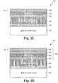
- structures 370 through 376 in Figures 3A through 3D illustrate the result of performing steps 270 through 276 of flowchart 200, respectively.
- structure 370 shows a semiconductor structure after processing step 270
- structure 372 shows structure 370 after the processing of step 272
- structure 374 shows structure 372 after the processing of step 274, and so forth.
- step 270 of flowchart 200 comprises providing a substrate under tensile stress by forming an AlN thick layer over an AlN nucleation layer over the substrate.
- Structure 370 of Figure 3A shows a cross-sectional view of a structure including a substrate, after completion of step 270 of flowchart 200 in Figure 2 .
- substrate 302 corresponds to substrate 102
- nucleation layer 304 corresponds to nucleation layer 104
- thick layer 306 corresponds to thick layer 106 in Figure 1 .
- substrate 302 is provided under tensile stress by forming nucleation layer 304 over substrate 302 and thick layer 306 over nucleation layer 304.
- Thick layer 306 can be formed, for example, by growing AlN in a high temperature process. It will be appreciated that the tensile stress is such that substrate 302 is provided substantially without cracking.
- stress region 320 is formed over substrate 302 to apply compressive stress to substrate 302.
- stress region 320 corresponds to a region of compositionally graded body 108 in Figure 1 , which is at an early stage of formation in structure 372.
- stress region 320 includes stress layers 322 and 324, which can correspond to respective compositionally graded layers in compositionally graded body 108.
- stress layers 322 and 324 can have varying compositions, for example, varying compositions of AlGaN.
- stress layer 322 comprises Al x Ga 1-x N and stress layer 324 comprises Al y Ga 1-y N, where each of subscripts "x" and "y” represents a different aluminum content in each respective layer.
- subscript "x” can be less than 1 and greater than 0.
- stress layer 324, formed on stress layer 322 has an aluminum content lower than stress layer 322.
- subscript "y” has a value less than the value of subscript "x,” such that stress region 320 includes layers of decreasing aluminum content.
- stress region 320 can apply compressive stress to substrate 302.
- substrate 302 is provided to step 272 under tensile stress.
- stress region 320 can reduce net tensile stress to substrate 302.
- stress layer 322 can apply compressive stress to substrate 302 to reduce net tensile stress to substrate 302 and stress layer 324 can apply sufficient additional compressive stress to provide substrate 302 under a net compressive stress upon completion of step 272.
- the result of step 272 of flowchart 200 is illustrated by structure 372 in Figure 3B .
- stress modulating region 326 is formed over stress region 320 to apply tensile stress to substrate 302.
- stress modulating region 326 corresponds to a region of compositionally graded body 108 in Figure 1 , which is at an intermediate stage of formation in structure 374.
- stress modulating region 326 comprises stress modulating layer 328, which is formed on stress layer 324 of stress region 320.
- stress modulating layer 328 comprises AlGaN having composition Al a Ga 1-a N where subscript "a” represents the aluminum content in stress modulating layer 328.
- stress modulating layer 328 has an aluminum content higher than stress layer 324, such that, stress modulating region 326 applies a tensile stress to substrate 302.
- subscript "a” can range from a value greater than the value of subscript "y", to 1.
- stress modulating region 328 can apply tensile stress to substrate 302, such that, substrate 302 is provided under, for example, a net tensile stress upon completion of step 274.
- the value of subscript "a” exceeds the value of subscript "x” as well as that of subscript "y”.
- step 274 of flowchart 200 is illustrated by structure 374 in Figure 3C .
- stress region 330 is formed over stress modulating region 326.
- stress region 330 corresponds to a region of compositionally graded body 308, which, in turn, corresponds to compositionally graded body 108 in Figure 1 .
- stress region 330 comprises stress layer 332 formed on stress modulating layer 328.
- stress layer 328 comprises AlGaN having composition AlbGai-bN where subscript "b" represents the aluminum content in stress layer 332.
- stress layer 332 has an aluminum content lower than stress modulating layer 328, such that, stress region 330 applies a compressive stress to substrate 302.
- the value of subscript "b" is less than that of subscript "a.”
- stress region 330 can apply a compressive stress to substrate 302 to provide substrate 302 under a reduced net tensile stress upon completion of step 276.
- the result of step 276 of flowchart 200 is illustrated by structure 376 in Figure 3D .
- the method illustrated in Figure 2 and Figures 3A through 3D provides for a compositionally graded body including a stress modulating region as part of a group III-V semiconductor device. Additional steps can be performed on structure 376 to fabricate structure 100 in Figure 1 .
- step 276 of flowchart 200 provides compositionally graded body 308, having a suitable lattice structure such that a buffer layer, for example buffer layer 110 in Figure 1 can be formed thereon without cracking or significant warping.
- the buffer layer can apply compressive stress to the substrate, for example, substrate 302.
- a thick buffer layer can apply compressive stress to the substrate in addition to the accumulated compressive stress produced by the layers used to transition between the substrate and the buffer layer, resulting in significant warping and/or cracking.
- stress modulating region 326 compositionally graded body 308 can modulate the stresses applied to substrate 302 to reduce the net applied stress, thereby reducing the incidence of significant warping and/or cracking. More particularly, stress modulating region 326 can apply tensile stress to substrate 302 compensate for excessive compressive stress applied by a thick buffer layer.
- structure 100 can be formed by fabricating HFET 112 on buffer layer 110 and cooling the wafer, which can apply additional tensile stress to substrate 302.
- each layer in structure 100 is controlled to result in a substantially stress free substrate 302 after wafer cooling.
- the stresses on substrate 302 can be balanced to limit the net stress applied to substrate 302.
- stress region 320 in Figure 3B comprises stress layer 322 and 324
- the number and thickness of stress layers in stress region 320 can be varied to adjust the stress applied to substrate 302.
- stress region 320 can comprise a single stress layer.
- the number and thickness of layers in stress modulating region 326 and stress region 330 can be varied.
- stress region 330 can be omitted.
- compositionally graded body 308 can comprise a plurality of stress modulating regions.
- a group III-V semiconductor device comprising:
- Said compositionally graded body may further include another stress layer having an aluminum content less than said third aluminum content over said stress modulating layer.
- Said third aluminum content may be greater than said first aluminum content.
- Said first stress layer, said second stress layer, and said stress modulating layer may each comprise AlGaN.
- Said active area may comprise a heterojunction field-effect transistor (HFET).
- HFET heterojunction field-effect transistor
- the present invention achieves a group III-V semiconductor device including a compositionally graded body having a least one stress modulating region.
- the compositionally graded body can modulate stress applied to a substrate to provide for a thick continuous buffer layer in the semiconductor device without significant warping and/or cracking.
- the semiconductor device can have enhanced breakdown voltage, which is particularly desirable in high power semiconductor devices.
Landscapes
- Junction Field-Effect Transistors (AREA)
- Recrystallisation Techniques (AREA)
Claims (13)
- Gruppe-III-V-Halbleitervorrichtung (100), umfassend:einen in seiner Zusammensetzung abgestuften Körper (108), der über dem Substrat (302) und unter einer Pufferschicht (110), die einen aktiven Bereich (112) der Gruppe-III-V-Halbleitervorrichtung (100) trägt, angeordnet ist;wobei der in seiner Zusammensetzung abgestufte Körper (108) umfasst:einen ersten Bereich (320), der Kompressionsspannung auf das Substrat ausübt, wobei der erste Bereich (320) eine erste Spannungsschicht (322) und eine zweite Spannungsschicht (324), die auf der ersten Spannungsschicht (322) gebildet ist, umfasst, wobei ein erster Aluminiumgehalt (x) der ersten Spannungsschicht (322) höher als ein zweiter Aluminiumgehalt (y) der zweiten Spannungsschicht (324) ist; undeinen spannungsmodulierenden Bereich (326) über dem ersten Bereich, wobei der spannungsmodulierende Bereich Zugspannung auf das Substrat (302) ausübt, wobei der spannungsmodulierende Bereich eine dritte Spannungsschicht (328) umfasst, die auf der zweiten Spannungsschicht (324) gebildet ist, wobei ein dritter Aluminiumgehalt (a) der dritten Spannungsschicht (328) höher als der erste und der zweite Aluminiumgehalt (x, y) ist.
- Gruppe-III-V-Halbleitervorrichtung (100) gemäß Anspruch 1, wobei der in seiner Zusammensetzung abgestufte Körper (108) ferner einen zweiten Bereich (332) über dem spannungsmodulierenden Bereich (326) umfasst, wobei der zweite Bereich (322) Kompressionsspannung auf das Substrat (302) ausübt.
- Gruppe-III-V-Halbleitervorrichtung (100) gemäß Anspruch 1, wobei das Substrat (302) Silicium umfasst.
- Gruppe-III-V-Halbleitervorrichtung (100) gemäß Anspruch 1, wobei die erste, die zweite und die dritte Spannungsschicht (322, 324, 328) AlGaN umfassen.
- Gruppe-III-V-Halbleitervorrichtung (100) gemäß Anspruch 1, wobei die Pufferschicht (110) eine kontinuierliche Schicht von Gruppe-III-V-Halbleitermaterial umfasst.
- Gruppe-III-V-Halbleitervorrichtung (100) gemäß Anspruch 1, wobei die Pufferschicht (110) Gan umfasst.
- Gruppe-III-V-Halbleitervorrichtung (100) gemäß Anspruch 1, wobei eine Dicke der Pufferschicht (110) größer als etwa 1,3 µm ist.
- Gruppe-III-V-Halbleitervorrichtung (100) gemäß Anspruch 1, wobei der aktive Bereich (112) einen Heteroübergang-Feldeffekttransistor (HFET) umfasst.
- Verfahren zur Herstellung einer Gruppe-III-V-Halbleitervorrichtung (100), wobei das Verfahren umfasst:Bereitstellen eines Substrats (302) für die Gruppe-III-V-Halbleitervorrichtung (100);Bilden eines ersten Bereichs (320) aus einem in seiner Zusammensetzung abgestuften Körper (108) über dem Substrat (302), um Kompressionsspannung auf das Substrat (302) auszuüben, wobei der erste Bereich (320) eine erste Spannungsschicht (322) und eine zweite Spannungsschicht (324), die auf der ersten Spannungsschicht (322) gebildet ist, umfasst, wobei ein erster Aluminiumgehalt (x) der ersten Spannungsschicht (322) höher als ein zweiter Aluminiumgehalt (y) der zweiten Spannungsschicht (324) ist;Bilden eines spannungsmodulierenden Bereichs (326) des in seiner Zusammensetzung abgestuften Körpers (108) über dem ersten Bereich, wobei der spannungsmodulierende Bereich (326) Zugspannung auf das Substrat ausübt, wobei der spannungsmodulierende Bereich (326) eine dritte Spannungsschicht (328) umfasst, die auf der zweiten Spannungsschicht (324) gebildet ist, wobei ein dritter Aluminiumgehalt (a) der dritten Spannungsschicht (328) höher als der erste und der zweite Aluminiumgehalt (x, y) ist.
- Verfahren gemäß Anspruch 9, ferner umfassend Bilden eines zweiten Bereichs (332) des in seiner Zusammensetzung abgestuften Körpers (108) über dem spannungsmodulierenden Bereich (326), wobei der zweite Bereich (332) Kompressionsspannung auf das Substrat (302) ausübt.
- Verfahren gemäß Anspruch 9, wobei das Bilden des ersten Bereichs (320) Bilden der ersten Spannungsschicht (322) über dem Substrat (302) umfasst.
- Verfahren gemäß Anspruch 9, ferner umfassend Bilden einer kontinuierlichen Pufferschicht über dem in seiner Zusammensetzung abgestuften Körper (108) und eines aktiven Bereichs (112) über der kontinuierlichen Pufferschicht.
- Verfahren gemäß Anspruch 12, wobei eine Dicke der kontinuierlichen Pufferschicht größer als etwa 1,3 µm ist.
Applications Claiming Priority (1)
| Application Number | Priority Date | Filing Date | Title |
|---|---|---|---|
| US12/928,946 US20120153351A1 (en) | 2010-12-21 | 2010-12-21 | Stress modulated group III-V semiconductor device and related method |
Publications (3)
| Publication Number | Publication Date |
|---|---|
| EP2469583A2 EP2469583A2 (de) | 2012-06-27 |
| EP2469583A3 EP2469583A3 (de) | 2013-09-18 |
| EP2469583B1 true EP2469583B1 (de) | 2019-05-22 |
Family
ID=45406396
Family Applications (1)
| Application Number | Title | Priority Date | Filing Date |
|---|---|---|---|
| EP11189846.6A Active EP2469583B1 (de) | 2010-12-21 | 2011-11-18 | Stress-modulierte Gruppe III-V-Halbleitervorrichtung und zugehöriges Verfahren |
Country Status (3)
| Country | Link |
|---|---|
| US (1) | US20120153351A1 (de) |
| EP (1) | EP2469583B1 (de) |
| JP (1) | JP5731367B2 (de) |
Families Citing this family (17)
| Publication number | Priority date | Publication date | Assignee | Title |
|---|---|---|---|---|
| US8957454B2 (en) | 2011-03-03 | 2015-02-17 | International Rectifier Corporation | III-Nitride semiconductor structures with strain absorbing interlayer transition modules |
| US8546849B2 (en) | 2011-05-04 | 2013-10-01 | International Rectifier Corporation | High voltage cascoded III-nitride rectifier package utilizing clips on package surface |
| US8604486B2 (en) * | 2011-06-10 | 2013-12-10 | International Rectifier Corporation | Enhancement mode group III-V high electron mobility transistor (HEMT) and method for fabrication |
| US9281388B2 (en) | 2011-07-15 | 2016-03-08 | Infineon Technologies Americas Corp. | Composite semiconductor device with a SOI substrate having an integrated diode |
| US8796738B2 (en) | 2011-09-21 | 2014-08-05 | International Rectifier Corporation | Group III-V device structure having a selectively reduced impurity concentration |
| US9583574B2 (en) * | 2012-09-28 | 2017-02-28 | Intel Corporation | Epitaxial buffer layers for group III-N transistors on silicon substrates |
| CN103123948A (zh) * | 2013-01-15 | 2013-05-29 | 中国电子科技集团公司第五十五研究所 | 低弯曲度硅基iii族氮化物外延片及生长方法 |
| US9142407B2 (en) * | 2013-01-16 | 2015-09-22 | Taiwan Semiconductor Manufacturing Company, Ltd. | Semiconductor structure having sets of III-V compound layers and method of forming the same |
| US9054027B2 (en) * | 2013-05-03 | 2015-06-09 | Texas Instruments Incorporated | III-nitride device and method having a gate isolating structure |
| US9673286B2 (en) | 2013-12-02 | 2017-06-06 | Infineon Technologies Americas Corp. | Group III-V transistor with semiconductor field plate |
| US9343562B2 (en) | 2013-12-06 | 2016-05-17 | Infineon Technologies Americas Corp. | Dual-gated group III-V merged transistor |
| KR20150085724A (ko) * | 2014-01-16 | 2015-07-24 | 엘지전자 주식회사 | 질화물 반도체 소자 및 그 제조 방법 |
| US10636899B2 (en) | 2016-11-15 | 2020-04-28 | Infineon Technologies Austria Ag | High electron mobility transistor with graded back-barrier region |
| US10720520B2 (en) * | 2017-06-21 | 2020-07-21 | Infineon Technologies Austria Ag | Method of controlling wafer bow in a type III-V semiconductor device |
| WO2021258293A1 (en) | 2020-06-23 | 2021-12-30 | Innoscience (Zhuhai) Technology Co., Ltd. | Semiconductor device structures and methods of manufacturing the same |
| US11942521B2 (en) | 2020-12-30 | 2024-03-26 | Innoscience (suzhou) Semiconductor Co., Ltd. | Epitaxial layers with discontinued aluminium content for III-nitride semiconductor |
| JPWO2023127520A1 (de) * | 2021-12-27 | 2023-07-06 |
Citations (1)
| Publication number | Priority date | Publication date | Assignee | Title |
|---|---|---|---|---|
| US20100243989A1 (en) * | 2009-03-26 | 2010-09-30 | Sumitomo Electric Device Innovations, Inc. | Semiconductor device |
Family Cites Families (16)
| Publication number | Priority date | Publication date | Assignee | Title |
|---|---|---|---|---|
| US5880491A (en) * | 1997-01-31 | 1999-03-09 | The United States Of America As Represented By The Secretary Of The Air Force | SiC/111-V-nitride heterostructures on SiC/SiO2 /Si for optoelectronic devices |
| TWI230978B (en) * | 2003-01-17 | 2005-04-11 | Sanken Electric Co Ltd | Semiconductor device and the manufacturing method thereof |
| JP4525894B2 (ja) * | 2003-11-21 | 2010-08-18 | サンケン電気株式会社 | 半導体素子形成用板状基体及びこの製造方法及びこれを使用した半導体素子 |
| US20050133816A1 (en) * | 2003-12-19 | 2005-06-23 | Zhaoyang Fan | III-nitride quantum-well field effect transistors |
| US7226850B2 (en) * | 2005-05-19 | 2007-06-05 | Raytheon Company | Gallium nitride high electron mobility transistor structure |
| US7491626B2 (en) * | 2005-06-20 | 2009-02-17 | Sensor Electronic Technology, Inc. | Layer growth using metal film and/or islands |
| JP2007088426A (ja) * | 2005-08-25 | 2007-04-05 | Furukawa Electric Co Ltd:The | 半導体電子デバイス |
| JP4751150B2 (ja) * | 2005-08-31 | 2011-08-17 | 株式会社東芝 | 窒化物系半導体装置 |
| US7547925B2 (en) * | 2005-11-14 | 2009-06-16 | Palo Alto Research Center Incorporated | Superlattice strain relief layer for semiconductor devices |
| EP1978550A4 (de) * | 2005-12-28 | 2009-07-22 | Nec Corp | Feldeffekttransistor und mehrschichtiger epitaxialfilm zur verwendung bei der herstellung eines feldeffekttransistors |
| JP5309451B2 (ja) * | 2007-02-19 | 2013-10-09 | サンケン電気株式会社 | 半導体ウエーハ及び半導体素子及び製造方法 |
| JP4592742B2 (ja) * | 2007-12-27 | 2010-12-08 | Dowaエレクトロニクス株式会社 | 半導体材料、半導体材料の製造方法及び半導体素子 |
| JP2010042981A (ja) * | 2008-07-17 | 2010-02-25 | Sumitomo Electric Ind Ltd | AlGaNバルク結晶の製造方法およびAlGaN基板の製造方法 |
| JP5367434B2 (ja) * | 2009-03-31 | 2013-12-11 | 住友電工デバイス・イノベーション株式会社 | 半導体装置の製造方法 |
| DE112010001589B4 (de) * | 2009-04-08 | 2024-11-28 | Efficient Power Conversion Corporation | Kompensierter GATE-MISFET |
| JP2011071356A (ja) * | 2009-09-26 | 2011-04-07 | Sanken Electric Co Ltd | 半導体装置 |
-
2010
- 2010-12-21 US US12/928,946 patent/US20120153351A1/en not_active Abandoned
-
2011
- 2011-11-18 EP EP11189846.6A patent/EP2469583B1/de active Active
- 2011-12-05 JP JP2011266254A patent/JP5731367B2/ja active Active
Patent Citations (1)
| Publication number | Priority date | Publication date | Assignee | Title |
|---|---|---|---|---|
| US20100243989A1 (en) * | 2009-03-26 | 2010-09-30 | Sumitomo Electric Device Innovations, Inc. | Semiconductor device |
Also Published As
| Publication number | Publication date |
|---|---|
| EP2469583A3 (de) | 2013-09-18 |
| US20120153351A1 (en) | 2012-06-21 |
| EP2469583A2 (de) | 2012-06-27 |
| JP5731367B2 (ja) | 2015-06-10 |
| JP2012134479A (ja) | 2012-07-12 |
Similar Documents
| Publication | Publication Date | Title |
|---|---|---|
| EP2469583B1 (de) | Stress-modulierte Gruppe III-V-Halbleitervorrichtung und zugehöriges Verfahren | |
| JP5503487B2 (ja) | 歪緩衝中間層を有するiii−v族半導体デバイス | |
| CN110544716B (zh) | Iii-n半导体结构及形成iii-n半导体结构的方法 | |
| US8633569B1 (en) | AlN inter-layers in III-N material grown on REO/silicon substrate | |
| JP2012191202A (ja) | 歪吸収中間層遷移モジュールを有するiii族窒化物半導体構造 | |
| US11114555B2 (en) | High electron mobility transistor device and methods for forming the same | |
| CN102549729A (zh) | 用于半导体衬底上的大面积的基于氮化镓或其它氮化物的结构的应力补偿 | |
| CN111406306B (zh) | 半导体装置的制造方法、半导体装置 | |
| KR20150085724A (ko) | 질화물 반도체 소자 및 그 제조 방법 | |
| US20170323960A1 (en) | Epitaxial wafer, semiconductor device, method for producing epitaxial wafer, and method for producing semiconductor device | |
| US8872308B2 (en) | AlN cap grown on GaN/REO/silicon substrate structure | |
| US9117671B2 (en) | Fabrication of III-nitride semiconductor device and related structures | |
| KR20150012119A (ko) | 질화물 반도체 소자 및 그 제조 방법 | |
| US10411124B2 (en) | Semiconductor component with protrusion propagation body and corresponding methods of manufacture | |
| CN112242435A (zh) | 半导体外延结构及其形成方法 | |
| US8823025B1 (en) | III-N material grown on AIO/AIN buffer on Si substrate | |
| KR20150000753A (ko) | 질화물 반도체 소자 및 그 제조 방법 | |
| KR20140139890A (ko) | 질화물 반도체 소자 및 그 제조 방법 | |
| US9401420B2 (en) | Semiconductor device | |
| CN111146269A (zh) | 高电子迁移率晶体管装置及其制造方法 | |
| US20220384580A1 (en) | Iii-n semiconductor structure and method of manufacturing same | |
| KR20150000752A (ko) | 질화물 반도체 소자 및 그 제조 방법 | |
| CN106783955B (zh) | 含有氮镓铝和氮镓铟的插入层的半导体器件及其制造方法 | |
| KR20140120519A (ko) | 질화물 반도체 소자 및 그 제조 방법 |
Legal Events
| Date | Code | Title | Description |
|---|---|---|---|
| AK | Designated contracting states |
Kind code of ref document: A2 Designated state(s): AL AT BE BG CH CY CZ DE DK EE ES FI FR GB GR HR HU IE IS IT LI LT LU LV MC MK MT NL NO PL PT RO RS SE SI SK SM TR |
|
| AX | Request for extension of the european patent |
Extension state: BA ME |
|
| PUAI | Public reference made under article 153(3) epc to a published international application that has entered the european phase |
Free format text: ORIGINAL CODE: 0009012 |
|
| PUAL | Search report despatched |
Free format text: ORIGINAL CODE: 0009013 |
|
| AK | Designated contracting states |
Kind code of ref document: A3 Designated state(s): AL AT BE BG CH CY CZ DE DK EE ES FI FR GB GR HR HU IE IS IT LI LT LU LV MC MK MT NL NO PL PT RO RS SE SI SK SM TR |
|
| AX | Request for extension of the european patent |
Extension state: BA ME |
|
| RIC1 | Information provided on ipc code assigned before grant |
Ipc: H01L 21/335 20060101AFI20130813BHEP Ipc: H01L 29/778 20060101ALI20130813BHEP Ipc: H01L 29/20 20060101ALI20130813BHEP |
|
| 17P | Request for examination filed |
Effective date: 20140318 |
|
| RBV | Designated contracting states (corrected) |
Designated state(s): AL AT BE BG CH CY CZ DE DK EE ES FI FR GB GR HR HU IE IS IT LI LT LU LV MC MK MT NL NO PL PT RO RS SE SI SK SM TR |
|
| 17Q | First examination report despatched |
Effective date: 20151104 |
|
| STAA | Information on the status of an ep patent application or granted ep patent |
Free format text: STATUS: EXAMINATION IS IN PROGRESS |
|
| RAP1 | Party data changed (applicant data changed or rights of an application transferred) |
Owner name: INFINEON TECHNOLOGIES AMERICAS CORP. |
|
| GRAP | Despatch of communication of intention to grant a patent |
Free format text: ORIGINAL CODE: EPIDOSNIGR1 |
|
| STAA | Information on the status of an ep patent application or granted ep patent |
Free format text: STATUS: GRANT OF PATENT IS INTENDED |
|
| RIC1 | Information provided on ipc code assigned before grant |
Ipc: H01L 21/335 20060101ALI20181102BHEP Ipc: H01L 29/778 20060101AFI20181102BHEP Ipc: H01L 29/20 20060101ALI20181102BHEP |
|
| INTG | Intention to grant announced |
Effective date: 20181206 |
|
| GRAS | Grant fee paid |
Free format text: ORIGINAL CODE: EPIDOSNIGR3 |
|
| GRAA | (expected) grant |
Free format text: ORIGINAL CODE: 0009210 |
|
| STAA | Information on the status of an ep patent application or granted ep patent |
Free format text: STATUS: THE PATENT HAS BEEN GRANTED |
|
| AK | Designated contracting states |
Kind code of ref document: B1 Designated state(s): AL AT BE BG CH CY CZ DE DK EE ES FI FR GB GR HR HU IE IS IT LI LT LU LV MC MK MT NL NO PL PT RO RS SE SI SK SM TR |
|
| REG | Reference to a national code |
Ref country code: GB Ref legal event code: FG4D |
|
| REG | Reference to a national code |
Ref country code: CH Ref legal event code: EP |
|
| REG | Reference to a national code |
Ref country code: IE Ref legal event code: FG4D |
|
| REG | Reference to a national code |
Ref country code: DE Ref legal event code: R096 Ref document number: 602011059145 Country of ref document: DE |
|
| REG | Reference to a national code |
Ref country code: AT Ref legal event code: REF Ref document number: 1137143 Country of ref document: AT Kind code of ref document: T Effective date: 20190615 |
|
| REG | Reference to a national code |
Ref country code: NL Ref legal event code: MP Effective date: 20190522 |
|
| REG | Reference to a national code |
Ref country code: LT Ref legal event code: MG4D |
|
| PG25 | Lapsed in a contracting state [announced via postgrant information from national office to epo] |
Ref country code: HR Free format text: LAPSE BECAUSE OF FAILURE TO SUBMIT A TRANSLATION OF THE DESCRIPTION OR TO PAY THE FEE WITHIN THE PRESCRIBED TIME-LIMIT Effective date: 20190522 Ref country code: NL Free format text: LAPSE BECAUSE OF FAILURE TO SUBMIT A TRANSLATION OF THE DESCRIPTION OR TO PAY THE FEE WITHIN THE PRESCRIBED TIME-LIMIT Effective date: 20190522 Ref country code: LT Free format text: LAPSE BECAUSE OF FAILURE TO SUBMIT A TRANSLATION OF THE DESCRIPTION OR TO PAY THE FEE WITHIN THE PRESCRIBED TIME-LIMIT Effective date: 20190522 Ref country code: FI Free format text: LAPSE BECAUSE OF FAILURE TO SUBMIT A TRANSLATION OF THE DESCRIPTION OR TO PAY THE FEE WITHIN THE PRESCRIBED TIME-LIMIT Effective date: 20190522 Ref country code: ES Free format text: LAPSE BECAUSE OF FAILURE TO SUBMIT A TRANSLATION OF THE DESCRIPTION OR TO PAY THE FEE WITHIN THE PRESCRIBED TIME-LIMIT Effective date: 20190522 Ref country code: NO Free format text: LAPSE BECAUSE OF FAILURE TO SUBMIT A TRANSLATION OF THE DESCRIPTION OR TO PAY THE FEE WITHIN THE PRESCRIBED TIME-LIMIT Effective date: 20190822 Ref country code: AL Free format text: LAPSE BECAUSE OF FAILURE TO SUBMIT A TRANSLATION OF THE DESCRIPTION OR TO PAY THE FEE WITHIN THE PRESCRIBED TIME-LIMIT Effective date: 20190522 Ref country code: PT Free format text: LAPSE BECAUSE OF FAILURE TO SUBMIT A TRANSLATION OF THE DESCRIPTION OR TO PAY THE FEE WITHIN THE PRESCRIBED TIME-LIMIT Effective date: 20190922 Ref country code: SE Free format text: LAPSE BECAUSE OF FAILURE TO SUBMIT A TRANSLATION OF THE DESCRIPTION OR TO PAY THE FEE WITHIN THE PRESCRIBED TIME-LIMIT Effective date: 20190522 |
|
| PG25 | Lapsed in a contracting state [announced via postgrant information from national office to epo] |
Ref country code: LV Free format text: LAPSE BECAUSE OF FAILURE TO SUBMIT A TRANSLATION OF THE DESCRIPTION OR TO PAY THE FEE WITHIN THE PRESCRIBED TIME-LIMIT Effective date: 20190522 Ref country code: BG Free format text: LAPSE BECAUSE OF FAILURE TO SUBMIT A TRANSLATION OF THE DESCRIPTION OR TO PAY THE FEE WITHIN THE PRESCRIBED TIME-LIMIT Effective date: 20190822 Ref country code: GR Free format text: LAPSE BECAUSE OF FAILURE TO SUBMIT A TRANSLATION OF THE DESCRIPTION OR TO PAY THE FEE WITHIN THE PRESCRIBED TIME-LIMIT Effective date: 20190823 Ref country code: RS Free format text: LAPSE BECAUSE OF FAILURE TO SUBMIT A TRANSLATION OF THE DESCRIPTION OR TO PAY THE FEE WITHIN THE PRESCRIBED TIME-LIMIT Effective date: 20190522 |
|
| REG | Reference to a national code |
Ref country code: AT Ref legal event code: MK05 Ref document number: 1137143 Country of ref document: AT Kind code of ref document: T Effective date: 20190522 |
|
| PG25 | Lapsed in a contracting state [announced via postgrant information from national office to epo] |
Ref country code: CZ Free format text: LAPSE BECAUSE OF FAILURE TO SUBMIT A TRANSLATION OF THE DESCRIPTION OR TO PAY THE FEE WITHIN THE PRESCRIBED TIME-LIMIT Effective date: 20190522 Ref country code: RO Free format text: LAPSE BECAUSE OF FAILURE TO SUBMIT A TRANSLATION OF THE DESCRIPTION OR TO PAY THE FEE WITHIN THE PRESCRIBED TIME-LIMIT Effective date: 20190522 Ref country code: EE Free format text: LAPSE BECAUSE OF FAILURE TO SUBMIT A TRANSLATION OF THE DESCRIPTION OR TO PAY THE FEE WITHIN THE PRESCRIBED TIME-LIMIT Effective date: 20190522 Ref country code: DK Free format text: LAPSE BECAUSE OF FAILURE TO SUBMIT A TRANSLATION OF THE DESCRIPTION OR TO PAY THE FEE WITHIN THE PRESCRIBED TIME-LIMIT Effective date: 20190522 Ref country code: AT Free format text: LAPSE BECAUSE OF FAILURE TO SUBMIT A TRANSLATION OF THE DESCRIPTION OR TO PAY THE FEE WITHIN THE PRESCRIBED TIME-LIMIT Effective date: 20190522 Ref country code: SK Free format text: LAPSE BECAUSE OF FAILURE TO SUBMIT A TRANSLATION OF THE DESCRIPTION OR TO PAY THE FEE WITHIN THE PRESCRIBED TIME-LIMIT Effective date: 20190522 |
|
| REG | Reference to a national code |
Ref country code: DE Ref legal event code: R097 Ref document number: 602011059145 Country of ref document: DE |
|
| PG25 | Lapsed in a contracting state [announced via postgrant information from national office to epo] |
Ref country code: IT Free format text: LAPSE BECAUSE OF FAILURE TO SUBMIT A TRANSLATION OF THE DESCRIPTION OR TO PAY THE FEE WITHIN THE PRESCRIBED TIME-LIMIT Effective date: 20190522 Ref country code: SM Free format text: LAPSE BECAUSE OF FAILURE TO SUBMIT A TRANSLATION OF THE DESCRIPTION OR TO PAY THE FEE WITHIN THE PRESCRIBED TIME-LIMIT Effective date: 20190522 |
|
| PLBE | No opposition filed within time limit |
Free format text: ORIGINAL CODE: 0009261 |
|
| STAA | Information on the status of an ep patent application or granted ep patent |
Free format text: STATUS: NO OPPOSITION FILED WITHIN TIME LIMIT |
|
| PG25 | Lapsed in a contracting state [announced via postgrant information from national office to epo] |
Ref country code: TR Free format text: LAPSE BECAUSE OF FAILURE TO SUBMIT A TRANSLATION OF THE DESCRIPTION OR TO PAY THE FEE WITHIN THE PRESCRIBED TIME-LIMIT Effective date: 20190522 |
|
| 26N | No opposition filed |
Effective date: 20200225 |
|
| PG25 | Lapsed in a contracting state [announced via postgrant information from national office to epo] |
Ref country code: PL Free format text: LAPSE BECAUSE OF FAILURE TO SUBMIT A TRANSLATION OF THE DESCRIPTION OR TO PAY THE FEE WITHIN THE PRESCRIBED TIME-LIMIT Effective date: 20190522 |
|
| PG25 | Lapsed in a contracting state [announced via postgrant information from national office to epo] |
Ref country code: SI Free format text: LAPSE BECAUSE OF FAILURE TO SUBMIT A TRANSLATION OF THE DESCRIPTION OR TO PAY THE FEE WITHIN THE PRESCRIBED TIME-LIMIT Effective date: 20190522 |
|
| REG | Reference to a national code |
Ref country code: CH Ref legal event code: PL |
|
| PG25 | Lapsed in a contracting state [announced via postgrant information from national office to epo] |
Ref country code: LU Free format text: LAPSE BECAUSE OF NON-PAYMENT OF DUE FEES Effective date: 20191118 Ref country code: MC Free format text: LAPSE BECAUSE OF FAILURE TO SUBMIT A TRANSLATION OF THE DESCRIPTION OR TO PAY THE FEE WITHIN THE PRESCRIBED TIME-LIMIT Effective date: 20190522 Ref country code: CH Free format text: LAPSE BECAUSE OF NON-PAYMENT OF DUE FEES Effective date: 20191130 Ref country code: LI Free format text: LAPSE BECAUSE OF NON-PAYMENT OF DUE FEES Effective date: 20191130 |
|
| REG | Reference to a national code |
Ref country code: BE Ref legal event code: MM Effective date: 20191130 |
|
| GBPC | Gb: european patent ceased through non-payment of renewal fee |
Effective date: 20191118 |
|
| PG25 | Lapsed in a contracting state [announced via postgrant information from national office to epo] |
Ref country code: GB Free format text: LAPSE BECAUSE OF NON-PAYMENT OF DUE FEES Effective date: 20191118 Ref country code: IE Free format text: LAPSE BECAUSE OF NON-PAYMENT OF DUE FEES Effective date: 20191118 Ref country code: FR Free format text: LAPSE BECAUSE OF NON-PAYMENT OF DUE FEES Effective date: 20191130 |
|
| PG25 | Lapsed in a contracting state [announced via postgrant information from national office to epo] |
Ref country code: BE Free format text: LAPSE BECAUSE OF NON-PAYMENT OF DUE FEES Effective date: 20191130 |
|
| PG25 | Lapsed in a contracting state [announced via postgrant information from national office to epo] |
Ref country code: CY Free format text: LAPSE BECAUSE OF FAILURE TO SUBMIT A TRANSLATION OF THE DESCRIPTION OR TO PAY THE FEE WITHIN THE PRESCRIBED TIME-LIMIT Effective date: 20190522 |
|
| PG25 | Lapsed in a contracting state [announced via postgrant information from national office to epo] |
Ref country code: IS Free format text: LAPSE BECAUSE OF FAILURE TO SUBMIT A TRANSLATION OF THE DESCRIPTION OR TO PAY THE FEE WITHIN THE PRESCRIBED TIME-LIMIT Effective date: 20190922 |
|
| PG25 | Lapsed in a contracting state [announced via postgrant information from national office to epo] |
Ref country code: HU Free format text: LAPSE BECAUSE OF FAILURE TO SUBMIT A TRANSLATION OF THE DESCRIPTION OR TO PAY THE FEE WITHIN THE PRESCRIBED TIME-LIMIT; INVALID AB INITIO Effective date: 20111118 Ref country code: MT Free format text: LAPSE BECAUSE OF FAILURE TO SUBMIT A TRANSLATION OF THE DESCRIPTION OR TO PAY THE FEE WITHIN THE PRESCRIBED TIME-LIMIT Effective date: 20190522 |
|
| PG25 | Lapsed in a contracting state [announced via postgrant information from national office to epo] |
Ref country code: MK Free format text: LAPSE BECAUSE OF FAILURE TO SUBMIT A TRANSLATION OF THE DESCRIPTION OR TO PAY THE FEE WITHIN THE PRESCRIBED TIME-LIMIT Effective date: 20190522 |
|
| P01 | Opt-out of the competence of the unified patent court (upc) registered |
Effective date: 20230528 |
|
| REG | Reference to a national code |
Ref country code: DE Ref legal event code: R079 Ref document number: 602011059145 Country of ref document: DE Free format text: PREVIOUS MAIN CLASS: H01L0021335000 Ipc: H10D0030010000 |
|
| PGFP | Annual fee paid to national office [announced via postgrant information from national office to epo] |
Ref country code: DE Payment date: 20260121 Year of fee payment: 15 |