EP2469979A2 - Stromrichter-Controller mit einem neuartigen Leistungsfaktorkorrekturmechanismus - Google Patents
Stromrichter-Controller mit einem neuartigen Leistungsfaktorkorrekturmechanismus Download PDFInfo
- Publication number
- EP2469979A2 EP2469979A2 EP11175556A EP11175556A EP2469979A2 EP 2469979 A2 EP2469979 A2 EP 2469979A2 EP 11175556 A EP11175556 A EP 11175556A EP 11175556 A EP11175556 A EP 11175556A EP 2469979 A2 EP2469979 A2 EP 2469979A2
- Authority
- EP
- European Patent Office
- Prior art keywords
- norm
- reference current
- refc
- signal
- line
- Prior art date
- Legal status (The legal status is an assumption and is not a legal conclusion. Google has not performed a legal analysis and makes no representation as to the accuracy of the status listed.)
- Withdrawn
Links
- 238000006243 chemical reaction Methods 0.000 title claims abstract description 37
- 238000012937 correction Methods 0.000 title claims abstract description 22
- 230000007246 mechanism Effects 0.000 title claims abstract description 22
- 230000007274 generation of a signal involved in cell-cell signaling Effects 0.000 claims abstract description 21
- 238000010606 normalization Methods 0.000 claims abstract description 18
- 238000010586 diagram Methods 0.000 description 5
- 238000000034 method Methods 0.000 description 4
- 230000001105 regulatory effect Effects 0.000 description 4
- 238000013461 design Methods 0.000 description 3
- 238000012986 modification Methods 0.000 description 2
- 230000004048 modification Effects 0.000 description 2
- 238000013459 approach Methods 0.000 description 1
- 230000008713 feedback mechanism Effects 0.000 description 1
- 238000012545 processing Methods 0.000 description 1
- 238000012552 review Methods 0.000 description 1
Images


Classifications
-
- H—ELECTRICITY
- H02—GENERATION; CONVERSION OR DISTRIBUTION OF ELECTRIC POWER
- H02M—APPARATUS FOR CONVERSION BETWEEN AC AND AC, BETWEEN AC AND DC, OR BETWEEN DC AND DC, AND FOR USE WITH MAINS OR SIMILAR POWER SUPPLY SYSTEMS; CONVERSION OF DC OR AC INPUT POWER INTO SURGE OUTPUT POWER; CONTROL OR REGULATION THEREOF
- H02M1/00—Details of apparatus for conversion
- H02M1/42—Circuits or arrangements for compensating for or adjusting power factor in converters or inverters
- H02M1/4208—Arrangements for improving power factor of AC input
- H02M1/4225—Arrangements for improving power factor of AC input using a non-isolated boost converter
-
- H—ELECTRICITY
- H05—ELECTRIC TECHNIQUES NOT OTHERWISE PROVIDED FOR
- H05B—ELECTRIC HEATING; ELECTRIC LIGHT SOURCES NOT OTHERWISE PROVIDED FOR; CIRCUIT ARRANGEMENTS FOR ELECTRIC LIGHT SOURCES, IN GENERAL
- H05B45/00—Circuit arrangements for operating light-emitting diodes [LED]
- H05B45/30—Driver circuits
- H05B45/37—Converter circuits
- H05B45/3725—Switched mode power supply [SMPS]
- H05B45/375—Switched mode power supply [SMPS] using buck topology
-
- H—ELECTRICITY
- H05—ELECTRIC TECHNIQUES NOT OTHERWISE PROVIDED FOR
- H05B—ELECTRIC HEATING; ELECTRIC LIGHT SOURCES NOT OTHERWISE PROVIDED FOR; CIRCUIT ARRANGEMENTS FOR ELECTRIC LIGHT SOURCES, IN GENERAL
- H05B45/00—Circuit arrangements for operating light-emitting diodes [LED]
- H05B45/30—Driver circuits
- H05B45/37—Converter circuits
- H05B45/3725—Switched mode power supply [SMPS]
- H05B45/38—Switched mode power supply [SMPS] using boost topology
-
- H—ELECTRICITY
- H05—ELECTRIC TECHNIQUES NOT OTHERWISE PROVIDED FOR
- H05B—ELECTRIC HEATING; ELECTRIC LIGHT SOURCES NOT OTHERWISE PROVIDED FOR; CIRCUIT ARRANGEMENTS FOR ELECTRIC LIGHT SOURCES, IN GENERAL
- H05B45/00—Circuit arrangements for operating light-emitting diodes [LED]
- H05B45/30—Driver circuits
- H05B45/37—Converter circuits
- H05B45/3725—Switched mode power supply [SMPS]
- H05B45/385—Switched mode power supply [SMPS] using flyback topology
-
- Y—GENERAL TAGGING OF NEW TECHNOLOGICAL DEVELOPMENTS; GENERAL TAGGING OF CROSS-SECTIONAL TECHNOLOGIES SPANNING OVER SEVERAL SECTIONS OF THE IPC; TECHNICAL SUBJECTS COVERED BY FORMER USPC CROSS-REFERENCE ART COLLECTIONS [XRACs] AND DIGESTS
- Y02—TECHNOLOGIES OR APPLICATIONS FOR MITIGATION OR ADAPTATION AGAINST CLIMATE CHANGE
- Y02B—CLIMATE CHANGE MITIGATION TECHNOLOGIES RELATED TO BUILDINGS, e.g. HOUSING, HOUSE APPLIANCES OR RELATED END-USER APPLICATIONS
- Y02B70/00—Technologies for an efficient end-user side electric power management and consumption
- Y02B70/10—Technologies improving the efficiency by using switched-mode power supplies [SMPS], i.e. efficient power electronics conversion e.g. power factor correction or reduction of losses in power supplies or efficient standby modes
Definitions
- the present invention relates to a power conversion controller, and more particularly to a power conversion controller capable of providing power factor correction for power conversion applications requiring load current regulation.
- FIG. 1 illustrates a power conversion application, in which a prior art controller 100 having a power factor correction mechanism is used to control a power conversion circuit 110 such that the waveform of an input current I IN of the power conversion circuit 110 is analog to that of a line voltage V LINE , and the average of the input current I IN is regulated to result in a DC output voltage V O for a load 120.
- the controller includes a combiner 101, an amplifier 102, a multiplier 103, and a gate drive signal generation unit 104.
- the combiner 101 is used to generate an error signal by subtracting V O with a reference voltage V REF .
- the amplifier 102 having a high DC gain and a cutoff frequency below 120 H z , is used to amplify the error signal with a negative gain to generate an amplitude adjusting signal A.
- the multiplier 103 is used to multiply the line voltage V LINE with the amplitude adjusting signal A to generate a reference current signal S REFC .
- the gate drive signal generation unit 104 is used to generate a gate drive signal V G to control the switching of the power conversion circuit 110, wherein the duty of the gate drive signal V G is determined according to a voltage comparison of the reference current signal S REFC and a current sensing signal S CS , which represents the input current I IN .
- the current sensing signal S CS When in operation, the current sensing signal S CS will follow the reference current signal S REFC , and the negative feedback mechanism will force V O to approach V REF . As such, if the line voltage V LINE is changed to a higher/lower level, the amplitude of the reference current signal S REFC will be adjusted by the amplitude adjusting signal A to a smaller/larger value to result in a lower/higher level of the current sensing signal S CS so as to regulate V O at V REF .
- the reference current signal S REFC of which the waveform is analog to that of the line voltage V LINE , and of which the amplitude is equal to the product of the amplitude adjusting signal A and the amplitude of the line voltage V LINE , is the key signal for achieving power factor correction and output voltage regulation at the same time.
- the present invention proposes a power conversion controller having a novel power factor correction mechanism for power conversion applications.
- the major objective of the present invention is to propose a power conversion controller having a novel power factor correction mechanism for a power conversion circuit, which can be of buck type, buck-boost type, or boost type etc..
- a power conversion controller having a novel power factor correction mechanism including:
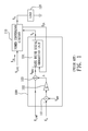
- FIG 2 illustrates a power conversion application, in which a controller 200 having a novel power factor correction mechanism according to a preferred embodiment of the present invention is used to control a power conversion circuit 230, such that the waveform of an input current I IN is analog to a line voltage V LINE , and the average of the output current I O is regulated according to a constant level to supply a load 240 with a corresponding output voltage V O .
- the controller 200 includes a reference current signal generation module 210-having a normalization unit 211 and a reference current generation unit 212-and a gate drive signal generation unit 220.
- the normalization unit 211 is used to generate a normalized signal V NORM according to the line voltage V LINE by multiplying the line voltage V LINE with a normalizing gain S G , wherein the normalizing gain S G is proportional to the reciprocal of the amplitude of the line voltage V LINE .
- the gate drive signal generation unit 220 is used to generate a gate drive signal V G , wherein the duty of the gate drive signal V G is determined by a voltage comparison of the reference current signal S REFC and a current sensing signal S CS .
- the reference current signal S REFC can be used as a peak reference current to determine the peak value of the current sensing signal S CD , or used as an average reference current to determine the average value of the current sensing signal S CS .
- the reference current signal S REFC so designed can render a constant average output current and an excellent power factor in the meantime for this type of application. The principle is elaborated as follows:
- V LINE expressed as V A sin ⁇ , 0° ⁇ 180° for a cycle of the full-wave rectified line voltage V LINE , and the switching frequency of V G is much higher than that of V LINE
- S REFC V NORM ⁇ S G as a peak reference current
- the reference current signal S REFC so designed can render a constant average output current and an excellent power factor in the meantime for this type of application. The principle is elaborated as follows:
- V LINE expressed as V A sin ⁇ , 0° ⁇ 180° for a cycle of the full-wave rectified line voltage V LINE , and the switching frequency of V G is much higher than that of V LINE
- S REFC V NORM as a peak reference current
- the input current is in phase with the line voltage V LINE , and the average output current over the cycle of the full-wave rectified line voltage V LINE is independent of the amplitude of V LINE .
- the buffer 412 can be replaced with another equivalent circuit-a feedthrough connection for example.
- the reference current signal S REFC so designed can render a constant average output current and an excellent power factor in the meantime for this type of application, and what is more, since the average output current will be independent of the output voltage, the design is especially suitable for a LED lighting application, of which the output voltage can vary a lot due to the spec variation of LEDs.
- the principle is elaborated as follows:
- V LINE expressed as V A sin ⁇ , 0° ⁇ 180° for a cycle of the full-wave rectified line voltage V LINE , and the switching frequency of V G is much higher than that of V LINE
- S REFC V NORM ⁇ V NORM as a peak reference current for boundary current mode operation
- I IN,avg represents the average of the input current I IN
- t ON is the active period of V G
- t OFF is the inactive period of V G
- K is a constant
- the average output current I O,avg can be expressed as I
- the input current is in phase with the line voltage V LINE , and the average output current over the cycle of the full-wave rectified line voltage V LINE is independent of the amplitude of V LINE and Vo.
- the reference current signal S REFC so designed can render a constant average output current and an excellent power factor in the meantime for this type of application, and what is more, since the average output current will be independent of the output voltage, the design is especially suitable for a LED lighting application, of which the output voltage can vary a lot due to the spec variation of LEDs.
- the principle is elaborated as follows:
- V LINE V A sin ⁇ , 0° ⁇ 180° for a cycle of the full-wave rectified line voltage V LINE , and the switching frequency of V G is much higher than that of V LINE
- S REFC V NORM ⁇ (V NORM + V O ⁇ S G ) as a peak reference current for boundary current mode operation
- V O V O (Ksin ⁇ ) 2 /2
- I IN,avg represents the average of the input current I IN , and K is a constant
- the reference current signal S REFC so designed can render a constant average output current and an excellent power factor in the meantime for this type of application, and what is more, since the average output current will be independent of the output voltage, the design is especially suitable for a LED lighting application, of which the output voltage can vary a lot due to the spec variation of LEDs.
- the principle is elaborated as follows:
- V LINE expressed as V A sin ⁇ , 0° ⁇ 180° for a cycle of the full-wave rectified line voltage V LINE , and the switching frequency of V G is much higher than that of V LINE
- S REFC V NORM ⁇ (V O S G ) as a peak reference current for boundary current mode operation
- V O V O (Ksin ⁇ ) 2
- I IN,avg represents the average of the input current I IN , and K is a constant
- the power conversion controller of the present invention having a normalization unit for processing a line voltage, a novel power factor correction mechanism for power converters of buck type, buck-boost type, boost type, fly-back type, etc. is proposed, and the large error amplifier needed in prior art is eliminated. Therefore, the present invention does improve the prior art controllers and is worthy of being granted a patent.
- the present invention herein enhances the performance than the conventional structure and further complies with the patent application requirements and is submitted to the Patent and Trademark Office for review and granting of the commensurate patent rights.
Landscapes
- Engineering & Computer Science (AREA)
- Power Engineering (AREA)
- Dc-Dc Converters (AREA)
- Power Conversion In General (AREA)
- Rectifiers (AREA)
Applications Claiming Priority (1)
| Application Number | Priority Date | Filing Date | Title |
|---|---|---|---|
| US12/953,219 US8541990B2 (en) | 2010-11-23 | 2010-11-23 | Power conversion controller having a novel power factor correction mechanism using line voltage normalization |
Publications (2)
| Publication Number | Publication Date |
|---|---|
| EP2469979A2 true EP2469979A2 (de) | 2012-06-27 |
| EP2469979A3 EP2469979A3 (de) | 2012-07-04 |
Family
ID=45463196
Family Applications (1)
| Application Number | Title | Priority Date | Filing Date |
|---|---|---|---|
| EP11175556A Withdrawn EP2469979A3 (de) | 2010-11-23 | 2011-07-27 | Stromrichter-Controller mit einem neuartigen Leistungsfaktorkorrekturmechanismus |
Country Status (3)
| Country | Link |
|---|---|
| US (1) | US8541990B2 (de) |
| EP (1) | EP2469979A3 (de) |
| JP (1) | JP2012115123A (de) |
Families Citing this family (12)
| Publication number | Priority date | Publication date | Assignee | Title |
|---|---|---|---|---|
| TWI396956B (zh) * | 2009-09-18 | 2013-05-21 | Richtek Technology Corp | 平均電流調節器及其驅動電路與平均電流調節方法 |
| US8390357B2 (en) * | 2011-05-27 | 2013-03-05 | Immense Advance Technology Corp. | Fixed dead time PFC controller |
| TWI492504B (zh) * | 2012-03-24 | 2015-07-11 | Richtek Technology Corp | 具有功率因子校正功能的電源供應電路,與用於其中之自動增益控制電路及其控制方法 |
| CN104322142B (zh) | 2012-05-18 | 2016-05-04 | 高周波热錬株式会社 | 感应加热系统、感应加热方法、输出监测装置、输出监测方法和感应加热装置 |
| US9130457B2 (en) * | 2012-10-24 | 2015-09-08 | Qualcomm Incorporated | Control logic for switches coupled to an inductor |
| US9548794B2 (en) | 2013-05-03 | 2017-01-17 | Cooper Technologies Company | Power factor correction for constant current input with power line communication |
| US9214855B2 (en) | 2013-05-03 | 2015-12-15 | Cooper Technologies Company | Active power factor correction circuit for a constant current power converter |
| US9000736B2 (en) * | 2013-05-03 | 2015-04-07 | Cooper Technologies Company | Power factor correction algorithm for arbitrary input waveform |
| US9190901B2 (en) | 2013-05-03 | 2015-11-17 | Cooper Technologies Company | Bridgeless boost power factor correction circuit for constant current input |
| TWI480716B (zh) * | 2013-11-27 | 2015-04-11 | Voltronic Power Technology Corp | 電流總諧波失真率控制電路及其方法 |
| US9214854B2 (en) | 2014-02-18 | 2015-12-15 | Voltronics Power Technology Corp. | Total harmonic current distortion control circuit and method thereof |
| CN114070015B (zh) * | 2020-08-05 | 2023-09-15 | 上海南芯半导体科技股份有限公司 | 一种功率器件的驱动控制方法及其驱动系统 |
Family Cites Families (12)
| Publication number | Priority date | Publication date | Assignee | Title |
|---|---|---|---|---|
| JP2001314085A (ja) * | 2000-04-28 | 2001-11-09 | Matsushita Electric Ind Co Ltd | 電源装置と、インバータ装置および空気調和機 |
| US7102340B1 (en) * | 2003-01-21 | 2006-09-05 | Microsemi Corporation | Dual-mode PFM boost converter |
| JP4778226B2 (ja) * | 2003-12-12 | 2011-09-21 | フィリップス ルミレッズ ライティング カンパニー リミテッド ライアビリティ カンパニー | Dc−dcコンバータ |
| US7266001B1 (en) * | 2004-03-19 | 2007-09-04 | Marvell International Ltd. | Method and apparatus for controlling power factor correction |
| US7733678B1 (en) * | 2004-03-19 | 2010-06-08 | Marvell International Ltd. | Power factor correction boost converter with continuous, discontinuous, or critical mode selection |
| US7812576B2 (en) * | 2004-09-24 | 2010-10-12 | Marvell World Trade Ltd. | Power factor control systems and methods |
| US7205749B2 (en) * | 2005-02-28 | 2007-04-17 | Texas Instruments Incorporated | Power line communication using power factor correction circuits |
| EP1977503B1 (de) * | 2005-12-12 | 2019-02-20 | Yaironit Ltd. | Vorrichtung, verfahren und system zur steuerung der wechselstrom-wechselstrom-umsetzung |
| US8237372B2 (en) * | 2006-12-04 | 2012-08-07 | Nxp B.V. | Electronic device for driving light emitting diodes |
| US7554473B2 (en) * | 2007-05-02 | 2009-06-30 | Cirrus Logic, Inc. | Control system using a nonlinear delta-sigma modulator with nonlinear process modeling |
| EP2166657A4 (de) * | 2007-07-09 | 2014-10-29 | Murata Manufacturing Co | Pfc-umsetzer |
| CN101237190A (zh) * | 2008-01-25 | 2008-08-06 | 魏其萃 | 用于功率电流变换器临界断续电流模式高精度平均输出电流控制方案 |
-
2010
- 2010-11-23 US US12/953,219 patent/US8541990B2/en not_active Expired - Fee Related
-
2011
- 2011-07-13 JP JP2011154612A patent/JP2012115123A/ja active Pending
- 2011-07-27 EP EP11175556A patent/EP2469979A3/de not_active Withdrawn
Non-Patent Citations (1)
| Title |
|---|
| None |
Also Published As
| Publication number | Publication date |
|---|---|
| JP2012115123A (ja) | 2012-06-14 |
| US8541990B2 (en) | 2013-09-24 |
| EP2469979A3 (de) | 2012-07-04 |
| US20120126759A1 (en) | 2012-05-24 |
Similar Documents
| Publication | Publication Date | Title |
|---|---|---|
| EP2469979A2 (de) | Stromrichter-Controller mit einem neuartigen Leistungsfaktorkorrekturmechanismus | |
| TWI645277B (zh) | 封包追蹤電源供應調控器 | |
| US8823346B2 (en) | System and method of feed forward for boost converters with improved power factor and reduced energy storage | |
| US9621028B2 (en) | Digitally controlled PFC converter with multiple discontinuous modes | |
| US7808299B2 (en) | Switching power converter with reduced switching losses | |
| CN111010026B (zh) | 用于电源的数字控制器、电源及操作电源的方法 | |
| EP3111542B1 (de) | Schaltnetzteil mit adaptiv randomisiertem spreizspektrum | |
| CN101350557B (zh) | 一种电源调整装置 | |
| EP2466740B1 (de) | Schaltung eines Hochleistungs-Tief-Hochsetzsperrwandlers und Steuerungsverfahren dafür | |
| US20060043942A1 (en) | Power converter apparatus and methods using output current feedforward control | |
| US8723494B2 (en) | Switching power converter current limit reference circuit | |
| US8300437B2 (en) | Multi-output DC-to-DC conversion apparatus with voltage-stabilizing function | |
| TWI484739B (zh) | 主動式功率因數校正電路及相關的控制器 | |
| US9847709B2 (en) | Switched-mode power supply device | |
| WO2015049716A1 (ja) | 力率改善回路 | |
| JP2013197098A (ja) | 照明駆動装置及びその方法 | |
| US20210257905A1 (en) | Power factor correction circuit with burst setting and method of operating the same | |
| US9774245B1 (en) | PFC switching power conversion circuit providing low total harmonic distortion | |
| US20120242298A1 (en) | Fixed-on-time controller utilizing an adaptive saw signal for discontinuous mode pfc power conversion | |
| US9515575B2 (en) | Power conversion apparatus and power conversion method | |
| US8390357B2 (en) | Fixed dead time PFC controller | |
| TWI473406B (zh) | 數位化前饋型寬輸出電壓之功率因數校正器及其方法 | |
| JP7666001B2 (ja) | 電力変換装置 | |
| US20140092644A1 (en) | Switching power supply device and method for circuit design of the switching power supply device | |
| US11482946B2 (en) | Electric power conversion device |
Legal Events
| Date | Code | Title | Description |
|---|---|---|---|
| PUAL | Search report despatched |
Free format text: ORIGINAL CODE: 0009013 |
|
| AK | Designated contracting states |
Kind code of ref document: A2 Designated state(s): AL AT BE BG CH CY CZ DE DK EE ES FI FR GB GR HR HU IE IS IT LI LT LU LV MC MK MT NL NO PL PT RO RS SE SI SK SM TR |
|
| AX | Request for extension of the european patent |
Extension state: BA ME |
|
| PUAI | Public reference made under article 153(3) epc to a published international application that has entered the european phase |
Free format text: ORIGINAL CODE: 0009012 |
|
| AK | Designated contracting states |
Kind code of ref document: A3 Designated state(s): AL AT BE BG CH CY CZ DE DK EE ES FI FR GB GR HR HU IE IS IT LI LT LU LV MC MK MT NL NO PL PT RO RS SE SI SK SM TR |
|
| AX | Request for extension of the european patent |
Extension state: BA ME |
|
| RIC1 | Information provided on ipc code assigned before grant |
Ipc: H02M 3/157 20060101ALI20120531BHEP Ipc: H05B 33/08 20060101AFI20120531BHEP |
|
| 17P | Request for examination filed |
Effective date: 20121221 |
|
| STAA | Information on the status of an ep patent application or granted ep patent |
Free format text: STATUS: THE APPLICATION HAS BEEN WITHDRAWN |
|
| 18W | Application withdrawn |
Effective date: 20140516 |