EP2472269A2 - Kapazitiver MEMS-Beschleunigungsmesser in der Ebene - Google Patents
Kapazitiver MEMS-Beschleunigungsmesser in der Ebene Download PDFInfo
- Publication number
- EP2472269A2 EP2472269A2 EP11250891A EP11250891A EP2472269A2 EP 2472269 A2 EP2472269 A2 EP 2472269A2 EP 11250891 A EP11250891 A EP 11250891A EP 11250891 A EP11250891 A EP 11250891A EP 2472269 A2 EP2472269 A2 EP 2472269A2
- Authority
- EP
- European Patent Office
- Prior art keywords
- substrate
- proof mass
- electrode
- capacitance
- electrodes
- Prior art date
- Legal status (The legal status is an assumption and is not a legal conclusion. Google has not performed a legal analysis and makes no representation as to the accuracy of the status listed.)
- Withdrawn
Links
- 239000000758 substrate Substances 0.000 claims abstract description 172
- 238000000034 method Methods 0.000 claims abstract description 42
- 230000001133 acceleration Effects 0.000 claims abstract description 28
- 230000008859 change Effects 0.000 claims abstract description 28
- 239000003990 capacitor Substances 0.000 claims description 35
- 230000008569 process Effects 0.000 claims description 12
- 239000000463 material Substances 0.000 claims description 8
- 230000004927 fusion Effects 0.000 claims description 7
- 230000035939 shock Effects 0.000 claims description 6
- 229910052710 silicon Inorganic materials 0.000 claims description 4
- 239000010703 silicon Substances 0.000 claims description 4
- KWYUFKZDYYNOTN-UHFFFAOYSA-M Potassium hydroxide Chemical compound [OH-].[K+] KWYUFKZDYYNOTN-UHFFFAOYSA-M 0.000 claims description 3
- 238000000708 deep reactive-ion etching Methods 0.000 claims 2
- 230000035945 sensitivity Effects 0.000 description 12
- 238000004519 manufacturing process Methods 0.000 description 10
- 230000007423 decrease Effects 0.000 description 4
- 230000001419 dependent effect Effects 0.000 description 4
- 238000005516 engineering process Methods 0.000 description 4
- 238000005259 measurement Methods 0.000 description 4
- XUIMIQQOPSSXEZ-UHFFFAOYSA-N Silicon Chemical compound [Si] XUIMIQQOPSSXEZ-UHFFFAOYSA-N 0.000 description 3
- 238000013016 damping Methods 0.000 description 3
- 238000001020 plasma etching Methods 0.000 description 3
- 238000010586 diagram Methods 0.000 description 2
- 238000005530 etching Methods 0.000 description 2
- 239000012212 insulator Substances 0.000 description 2
- 230000005486 microgravity Effects 0.000 description 2
- 238000005459 micromachining Methods 0.000 description 2
- 239000007787 solid Substances 0.000 description 2
- 238000005452 bending Methods 0.000 description 1
- 230000009286 beneficial effect Effects 0.000 description 1
- 230000008878 coupling Effects 0.000 description 1
- 238000010168 coupling process Methods 0.000 description 1
- 238000005859 coupling reaction Methods 0.000 description 1
- 238000005336 cracking Methods 0.000 description 1
- 238000000151 deposition Methods 0.000 description 1
- 238000006073 displacement reaction Methods 0.000 description 1
- 230000005496 eutectics Effects 0.000 description 1
- 239000011521 glass Substances 0.000 description 1
- 230000005484 gravity Effects 0.000 description 1
- 238000012986 modification Methods 0.000 description 1
- 230000004048 modification Effects 0.000 description 1
- 229910021420 polycrystalline silicon Inorganic materials 0.000 description 1
- 229920005591 polysilicon Polymers 0.000 description 1
- 230000004044 response Effects 0.000 description 1
- 239000004065 semiconductor Substances 0.000 description 1
- 238000009987 spinning Methods 0.000 description 1
- 238000009966 trimming Methods 0.000 description 1
Images



Classifications
-
- G—PHYSICS
- G01—MEASURING; TESTING
- G01P—MEASURING LINEAR OR ANGULAR SPEED, ACCELERATION, DECELERATION, OR SHOCK; INDICATING PRESENCE, ABSENCE, OR DIRECTION, OF MOVEMENT
- G01P15/00—Measuring acceleration; Measuring deceleration; Measuring shock, i.e. sudden change of acceleration
- G01P15/02—Measuring acceleration; Measuring deceleration; Measuring shock, i.e. sudden change of acceleration by making use of inertia forces using solid seismic masses
- G01P15/08—Measuring acceleration; Measuring deceleration; Measuring shock, i.e. sudden change of acceleration by making use of inertia forces using solid seismic masses with conversion into electric or magnetic values
- G01P15/125—Measuring acceleration; Measuring deceleration; Measuring shock, i.e. sudden change of acceleration by making use of inertia forces using solid seismic masses with conversion into electric or magnetic values by capacitive pick-up
-
- G—PHYSICS
- G01—MEASURING; TESTING
- G01P—MEASURING LINEAR OR ANGULAR SPEED, ACCELERATION, DECELERATION, OR SHOCK; INDICATING PRESENCE, ABSENCE, OR DIRECTION, OF MOVEMENT
- G01P15/00—Measuring acceleration; Measuring deceleration; Measuring shock, i.e. sudden change of acceleration
- G01P15/02—Measuring acceleration; Measuring deceleration; Measuring shock, i.e. sudden change of acceleration by making use of inertia forces using solid seismic masses
- G01P15/08—Measuring acceleration; Measuring deceleration; Measuring shock, i.e. sudden change of acceleration by making use of inertia forces using solid seismic masses with conversion into electric or magnetic values
- G01P15/0802—Details
-
- G—PHYSICS
- G01—MEASURING; TESTING
- G01P—MEASURING LINEAR OR ANGULAR SPEED, ACCELERATION, DECELERATION, OR SHOCK; INDICATING PRESENCE, ABSENCE, OR DIRECTION, OF MOVEMENT
- G01P15/00—Measuring acceleration; Measuring deceleration; Measuring shock, i.e. sudden change of acceleration
- G01P15/02—Measuring acceleration; Measuring deceleration; Measuring shock, i.e. sudden change of acceleration by making use of inertia forces using solid seismic masses
- G01P15/08—Measuring acceleration; Measuring deceleration; Measuring shock, i.e. sudden change of acceleration by making use of inertia forces using solid seismic masses with conversion into electric or magnetic values
- G01P2015/0805—Measuring acceleration; Measuring deceleration; Measuring shock, i.e. sudden change of acceleration by making use of inertia forces using solid seismic masses with conversion into electric or magnetic values being provided with a particular type of spring-mass-system for defining the displacement of a seismic mass due to an external acceleration
- G01P2015/0808—Measuring acceleration; Measuring deceleration; Measuring shock, i.e. sudden change of acceleration by making use of inertia forces using solid seismic masses with conversion into electric or magnetic values being provided with a particular type of spring-mass-system for defining the displacement of a seismic mass due to an external acceleration for defining in-plane movement of the mass, i.e. movement of the mass in the plane of the substrate
- G01P2015/0811—Measuring acceleration; Measuring deceleration; Measuring shock, i.e. sudden change of acceleration by making use of inertia forces using solid seismic masses with conversion into electric or magnetic values being provided with a particular type of spring-mass-system for defining the displacement of a seismic mass due to an external acceleration for defining in-plane movement of the mass, i.e. movement of the mass in the plane of the substrate for one single degree of freedom of movement of the mass
- G01P2015/0814—Measuring acceleration; Measuring deceleration; Measuring shock, i.e. sudden change of acceleration by making use of inertia forces using solid seismic masses with conversion into electric or magnetic values being provided with a particular type of spring-mass-system for defining the displacement of a seismic mass due to an external acceleration for defining in-plane movement of the mass, i.e. movement of the mass in the plane of the substrate for one single degree of freedom of movement of the mass for translational movement of the mass, e.g. shuttle type
Definitions
- the present invention relates to accelerometers and other force-sensing devices, and more particularly to a gun-hard, in-plane MEMS capacitive accelerometer that includes a proof mass formed from a single piece of material positioned above a plurality of electrodes on a substrate.
- a gun-hard, in-plane MEMS capacitive accelerometer that includes a proof mass formed from a single piece of material positioned above a plurality of electrodes on a substrate.
- the proof mass moves in a direction parallel to the upper surfaces of the substrate, changing the capacitance between the proof mass and the substrate. This change in capacitance can be used to measure the displacement and to determine the acceleration of an object to which the substrate is attached.
- Accelerometers are a critical component in the Inertial Measurement Units (IMUs) commonly used in navigation and guidance systems for all types of vehicles.
- IMUs Inertial Measurement Units
- a typical IMU consists of three equal modules, each including a linear accelerometer, a gyroscopic rotational rate sensor, and associated electronics. These three-axis IMUs are used for navigation, guidance, and data-measurement systems in aerospace applications ranging from aircraft and spacecraft, to precision-guided missiles and artillery rounds. In many of these applications, the IMU is exposed to extreme vibrations and shock loads; it must be designed to withstand these harsh conditions.
- Inertial Measurement Units capable of surviving harsh shock loads are known as gun-hard IMUs. These high-performance IMUs remain fully functional even when exposed to forces that are thousands of times stronger than the pull of gravity. Use of high-performance accelerometers and other components allow for reliable, consistent, and precise guidance of the vehicle or projectile on which the IMU is installed.
- High-performance accelerometers with near micro-gravity resolution, high sensitivity, high linearity, and low bias drift are critical for use in gun-hard IMUs.
- IMUs included large mechanical accelerometers and conventional spinning mass gyroscopes.
- MEMS microelectromechanical systems
- Silicon capacitive accelerometers have several advantages that make them very attractive for gun-hard IMUs. Silicon capacitive accelerometers have high sensitivity, good direct current response and noise performance, low drift, low temperature sensitivity, low power dissipation, and a simple structure. It would be beneficial to have a gun-hard, high-performance, three-axis accelerometer built on a single chip using MEMS fabrication techniques. But this requires building both out-of-plane and in-plane accelerometers on the chip using the same fabrication techniques.
- Known in-plane accelerometer configurations include MEMS comb-finger accelerometers, where the sensing gaps are formed between side walls and the sensitivity is determined by the size of the sensing gaps.
- a conventional MEMS comb-finger accelerometer is shown in Fig. 7 and designated generally by numeral 700.
- Accelerometer 700 includes a proof mass or sensing plate 702 attached by springs to two anchors 704 and having a plurality of movable fingers 706. Movable fingers 706 are interdigitated with a plurality of fixed fingers 708, with a lateral gap formed between the movable and fixed fingers.
- the minimum size of the lateral gap is limited to between about 1/10th and 1/15th of the plate thickness by the aspect ratio of the Dry Reactive Ion Etching (DRIE) technology used to fabricate in-plane accelerometer 700.
- DRIE Dry Reactive Ion Etching
- Existing DRIE technology is only capable of producing gaps as small as 10 ⁇ m; it is not possible to fabricate a MEMS comb-finger, in-plane accelerometer using this technique for a plate that is 75 ⁇ m thick.
- the conventional comb-finger accelerometer configuration has inherent nonlinearity issues. To improve linearity, the change in the lateral gap must be limited to a small range, which leads to a small differential capacitance output.
- a system for determining in-plane acceleration of an object including an in-plane accelerometer with a substrate rigidly attached to an object, and a proof mass-formed from a single piece of material-movably positioned a predetermined distance above the substrate.
- a plurality of first substrate electrodes may extend upward from the substrate and alternate with a plurality of second substrate electrodes that also extend upward from the substrate.
- Each substrate electrode has a planar upper surface.
- the plurality of first substrate electrodes may be electrically connected to one another, and the plurality of second substrate electrodes are electrically connected to one another.
- the proof mass may include a plurality of electrode protrusions extending downward from the proof mass to form a gap of varying height between the proof mass and the substrate.
- a first capacitor may be formed between the proof mass and the plurality of first substrate electrodes, and a second capacitor may be formed between the proof mass and the plurality of second substrate electrodes.
- the proof mass may be configured to be held in an equilibrium position when the velocity of the object is constant, with each of the plurality of electrode protrusions being positioned over a portion of one first substrate electrode and a portion of an adjacent second substrate electrode when the proof mass is in the equilibrium position.
- the proof mass may be configured to move in a direction parallel to the upper surfaces of each of the plurality of substrate electrodes when the object is accelerating. This may result in a change in the area of the gap between the upper surface of each of the substrate electrodes and the proof mass.
- a method of measuring in-plane acceleration of an object includes the steps of: rigidly attaching a substrate to an object; securing a proof mass in an equilibrium position a predetermined distance above the substrate to form a gap of varying height between the proof mass and the substrate; forming a first differential capacitor between the proof mass and a plurality of first substrate electrodes, and forming a second differential capacitor between the proof mass and a plurality of second substrate electrodes, wherein the first substrate electrodes and second substrate electrodes are alternatingly positioned on the substrate; displacing the proof mass from the equilibrium position in a direction parallel to a planar upper face of the substrate electrodes by applying an acceleration force to the object; measuring a first change in capacitance in the first differential capacitor; measuring a second change in capacitance in the second differential capacitor; and using a circuit to convert the measured changes in capacitance to a voltage representing acceleration of the object.
- An additional method of measuring in-plane acceleration of an object includes the steps of: rigidly attaching a substrate to an object; suspending a proof mass above the substrate, the proof mass being constrained to move in only one direction; forming a differential capacitor between the proof mass and the substrate, wherein the proof mass includes a plurality of electrode protrusions with each electrode protrusion centered above two substrate electrodes such that an area between an upper planar surface of each substrate electrode and the proof mass changes when the proof mass moves in a direction parallel to the upper planar surfaces of the substrate electrode; displacing the proof mass by applying an acceleration force to the object; measuring a change in capacitance between each substrate electrode and the proof mass; using a circuit to convert the measured change in capacitance to a voltage representing acceleration of the object; outputting a voltage from the circuit that is proportional to the change in area between the upper planar surface of each substrate electrode and the proof mass.
- the out-of-plane accelerometer described in that application uses a 75 ⁇ m (micron) silicon-on-insulator (SOI) layer as a sensing structure.
- SOI silicon-on-insulator
- Such asymmetric solid/hollow proof mass sensor structures exhibit higher sensitivity than surface micromachined rocking structures because of the relatively thick proof mass and narrow vertical gap between the proof mass and a substrate of the out-of-plane pendulous accelerometer.
- This disclosure describes an in-plane accelerometer that can be fabricated using techniques similar to those used to fabricate the out-of-plane pendulous accelerometer. Examples of these fabrication techniques are disclosed in U.S. Patent No. 7,736,931, issued June 15, 2010 and titled "Wafer Process Flow for a High Performance MEMS Accelerometer, which is also incorporated herein by reference.
- This disclosure describes a gun-hard, in-plane MEMS accelerometer that measures differential capacitance as a proof mass positioned above a substrate moves in a direction parallel to an upper surface of the substrate.
- To obtain a high-performance, gun-hard, low-noise, in-plane accelerometer it is necessary to increase the proof mass size, reduce the sensing gaps, and reduce damping. But in a thick proof mass MEMS process, it is much more difficult to reduce the lateral gap typical in an in-plane accelerometer, as shown in the conventional in-line accelerometer of Fig. 7 , than it is to reduce the vertical gap typical in an out-of-plane accelerometer.
- the present invention is an offset comb-finger, in-plane accelerometer that can be fabricated using the same technology used for fabricating out-of-plane accelerometers.
- the in-plane accelerometer may use a thick proof mass and a vertical gap that can be made as small as 1.0 ⁇ m. Because it uses area change instead of gap change to measure capacitance, the in-plane accelerometer described in this disclosure has a linear change over acceleration. It is also suitable for open loop accelerometer design.
- the fabrication process flow is the same as that of the existing out-of-plane accelerometer, which allows the in-plane accelerometer and out-of-plane accelerometer to be fabricated on a single chip using the same fabrication techniques.
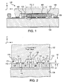
- In-plane accelerometer 100 includes a proof mass 102, a substrate 104, and a topping wafer 106.
- the topping wafer provides shock protection for proof mass 102 and may be glass frit bonded to substrate 104.
- a fusion bond or a eutectic bond could also be used to bond topping wafer 106 to substrate 104.
- Accelerometer 100 may also include a guard ring 105 surrounding proof mass 102.
- Substrate 104 is rigidly attached to an object, while proof mass 102 is suspended above substrate 104 by springs 103 or by other suitable means, which allows accelerometer 100 to determine the acceleration of the object by measuring the differential change in capacitance between proof mass 102 and substrate 104.
- proof mass 102 may be movably attached to a wafer that is in turn fusion bonded to substrate 104.
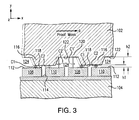
- Fig. 2 is a detailed view of a portion of accelerometer 100, showing details of proof mass 102 and substrate 104.
- Substrate 104 may comprise a silicon-on-insulator (SOI) material.
- substrate 104 includes a plurality of first substrate electrodes 108 extending upward from substrate 104, and a plurality of second substrate electrodes 110, which also extend upward from substrate 104.
- the first and second substrate electrodes 108, 110 are arranged in an alternating pattern on substrate 104. In other words, for each of first substrate electrodes 108, the immediately adjacent substrate electrode is one of the second substrate electrodes 110, and for each of the second substrate electrodes 110, the immediately adjacent substrate electrode is once of the first substrate electrodes 108.
- Each of the first and second substrate electrodes have a planar upper surface 112 a predetermined distance above a planar upper surface 114 of substrate 104.
- Planar upper surfaces 112 of the first and second substrate electrodes 108, 110 are positioned parallel to the planar upper surface 114 of substrate 104.
- substrate electrodes 108, 110 have a height ranging from about 0.5 ⁇ m to about 4 ⁇ m.
- Fig. 2 also shows a plurality of electrode protrusions 116 which extend downward from proof mass 102 toward substrate 104.
- Proof mass 102 is formed from a single piece of material.
- the material is a semiconductor such as silicon. Because proof mass 102 is formed from a single piece of material, these protrusions 116 are formed by removing material from proof mass 102; the protrusions are an integral part of proof mass 102 and are not formed separately.
- Each electrode protrusion 116 has a lower planar surface 118. In the exemplary embodiment shown in Figs.
- electrode protrusions 116 are formed using a potassium hydroxide (KOH) etching process, which produces sidewalls on each electrode protrusion 116 with an angle of 54.7° with respect to lower planar surface 118.
- KOH potassium hydroxide
- a valley 120 is formed in an area adjacent each electrode protrusion 116, for example, between two electrode protrusions 116.
- Valley 120 includes a planar valley surface 122 that is parallel to lower planar surfaces 118 of the electrode protrusions 116.
- Proof mass 102 of accelerometer 100 is positioned a predetermined distance above substrate 104 such that a gap 124 is formed between proof mass 102 and substrate 104. Because electrode protrusions 116 extend downward and because first and second substrate electrodes 108, 110 are positioned on top of the substrate, the height of gap 124 between proof mass 102 and substrate 104 varies along the length L of proof mass 102.
- Proof mass 102 is movably positioned above substrate 104 by one or more springs 103.
- the design of the springs is critical for obtaining high sensitivity and low cross talk.
- Cross talk is the undesired capacitive coupling from one circuit to another. Because in-plane accelerometer 100 is designed to measure acceleration along a single axis, it is designed to eliminate cross talk.
- the key trade-off in the spring design is balancing sensitivity with cross talk.
- the springs should be flexible in the x-direction but stiff in the z-direction and in the y-direction.
- the x-direction extends along the length of proof mass 102, parallel to lower planar surfaces of electrode protrusions 116.
- the y-direction is perpendicular to the x-direction, and the z-direction extends directly out of the page as shown in Fig. 2 .
- the springs should be very thin in the x-direction and relatively thick in the y- and z-directions.
- the width of the springs in the x-direction is the same as the width of proof mass 102 in the x-direction. In other words, the spring and the proof mass have the same thickness.
- capacitive sensitivity is dependent on the first-mode resonant frequency.
- the lower the first-mode frequency the higher the capacitive sensitivity.
- Cross talk is dependent on the second-mode resonant frequency; the higher the second-mode frequency, the lower the cross talk.
- capacitive sensitivity is fixed, a thinner spring can achieve lower cross talk.
- the minimum width of the spring is limited by capabilities of the fabrication process used, for example, by the aspect ratio of a Dry Reactive Ion Etch (DRIE) process.
- DRIE Dry Reactive Ion Etch
- proof mass 102 is held in position above substrate 104 by springs 130 such that each of the plurality of electrode protrusions overlaps a portion of one first substrate electrode 108 and a portion of the adjacent second substrate electrode 110.
- first substrate electrodes 108 are electrically connected to one another, and each of the second substrate electrodes are likewise electrically connected to one another.
- a first capacitor is formed between proof mass 102 and the plurality of first substrate electrodes 108
- a second capacitor is formed between proof mass 102 and the plurality of second substrate electrodes 110.
- substrate electrodes 108, 110 are arranged symmetrically, such that when the acceleration of the object is equal to zero, that is, when proof mass 102 is in the equilibrium position, the capacitance of the first capacitor is equal to the capacitance of the second capacitor.
- each first substrate electrode 108 has a first capacitance C 1 between lower planar surface 118 of the electrode protrusion and planar upper surface 112 of first substrate electrode 108, and a second capacitance C1' between valley planar surface 122 of proof mass 102 and planar upper surface 112 of first substrate electrode 108.
- each second electrode protrusion has a first capacitance C2 between lower planar surface 118 of the electrode protrusion and planar upper surface 112 of second substrate electrode 110, and a second capacitance C2' between valley planar surface 122 of proof mass 102 and planar upper surface 112 of second substrate electrode 110.
- proof mass 102 moves from the equilibrium position shown in Fig. 2 , to a second position, shown in Fig. 3 .
- the capacitance C2 increases and capacitance C 1 decreases due to the area change in gap 124 between proof mass 102 and substrate electrodes 108, 110.
- capacitance C2' decreases and capacitance C1' increases as the proof mass moves from the equilibrium position.
- gap 124 varies along the length L of proof mass 102.
- gap 124 may have a first height h1 between lower planar surfaces 118 of electrode protrusions 116 and planar upper surfaces 112 of substrate electrodes 108, 110; and a second height h2 between valley planar surfaces 122 and planar upper surfaces 112 of substrate electrodes 108, 110.
- Second height h2 is much greater than first height h1.
- h2 may be between ten and twenty times greater than h1.
- Capacitance decreases with distance between electrodes; as a result of the height difference between h1 and h2, capacitance C1 is much greater than C1' and capacitance C2 is much greater than C2'. So the overall differential changes in capacitance are dominated by C1 and C2.
- accelerometer 100 There are several advantages of the structure described above for accelerometer 100. First, if a thick proof mass (greater than 50 ⁇ m) is used, the small height h1 of gap 124 is more easily obtained with known process capabilities than are the lateral gaps of prior art in-line accelerometers. Additionally there is no stiction problem at high-g loads in the offset comb-finger in-line accelerometer 100 described above. Accelerometer 100 is also more robust than a lateral comb-finger structure and suitable for use in gun-hard devices.
- Fig. 4 illustrates an equivalent circuit to the circuit created by in-plane accelerometer 100.
- the circuit includes two capacitors.
- a first capacitor with capacitance C1 is formed between proof mass 102 and first substrate electrodes 108.
- a second capacitor with capacitance C2 is formed between proof mass 102 and second substrate electrodes 110.
- each of the first substrate electrodes 108 are electically connected to one another.
- each of the second substrate electrodes 110 are electrically connected.
- the nominal capacitance values of C 1 and C2 are equal at about 7.5 pF (picofarads) when proof mass 102 and substrate electrodes 108, 110 are symmetrically positioned-that is, when each electrode protrusion 116 is aligned above first substrate electrode 108 and second substrate electrode 110 such that the area of overlap between a first substrate electrode 108 and an electrode protrusion 116 is the same as the overlap between the adjacent second substrate electrode 110 and the same electrode protrusion 116.
- Fig. 2 shows proof mass 102 with electrode protrusions 116 symmetrically positioned above substrate electrodes 108, 110.
- a difference in capacitive values for C1 and C2 can be caused by a misalignment of the fusion bond between proof mass 102 and substrate 104.
- the tolerance of the current fusion bond misalignment is about 5 ⁇ m, meaning that the nominal capacitance of C1 and C2 could vary from 2.75 to 13.75 pF.
- the total capacitance, Csum, of accelerometer 100 is equal to the sum of capacitance C 1 and capacitance C2.
- the common mode capacitive change in C1 and C2 is therefore canceled; only differential change will be amplified. This means that the z-axis cross talk, which leads to common capacitive change, is minimized.
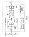
- Fig 5 is an example of a circuit that may interface with in-plane accelerometer 100 to convert the measured difference in capacitance between proof mass 102 and substrate electrodes 108, 110 to an output voltage representing the acceleration of substrate 104, and by extension, the acceleration of the object to which the substrate is rigidly attached.
- the circuit may included a built-in capacitor array that can be used to balance C1 and C2 and to minimize the bias off-set.
- C1_trim provides 0.2-10 pF range for trimming.
- the capacitor array includes 9 bits of programmability in 19 fF +/- 20% steps.
- the primary natural resonant frequency of the proof mass is 1890 Hz, and the maximum beam bending along the x-axis is about 2.1 ⁇ m. Because the fusion bond misalignment tolerance is 5 ⁇ m, the minimum overlap between electrode protrusions 116 and substrate electrodes 108, 110 has to be greater than 2.1 ⁇ m. So the overlap in layout design should be larger than 7.1 ⁇ m.
- the width of each substrate electrode 108, 110 is 15 ⁇ m and the width of electrode protrusion 116 is 20 ⁇ m to ensure that the substrate electrodes are covered by electrode protrusion 116, even with up to 5 ⁇ m of misalignment. If the misalignment tolerance can be reduced, then the width of the substrate electrodes can also be reduced. In that case, the number of substrate electrodes can be increased, which will increase the sensitivity of accelerometer 100.
- a misalignment tolerance of less than 1 ⁇ m can be achieved using a fusion-bond-alignment machine, such as the EVG SmartView® Automated Bond Alignment System, available from the EV Group of Austria.
- In-plane accelerometer 600 is similar to the previously described in-plane accelerometer, and includes a proof mass 602, a substrate 604 and a topping wafer 606. As shown, proof mass 602 is movable positioned above the substrate.
- Substrate 604 includes a plurality of first substrate electrodes 608, which are electrically connected to one another, and a plurality of second substrate electrodes 610, which are also electrically connected to one another, similar to the electrodes described with regard to in-plane accelerometer 100.
- in-plane accelerometer 600 has a plurality of electrode fingers 616 formed by a Dry Reactive Ion Etching (DRIE) process rather than by a potassium hydroxide (KOH) etching process.
- DRIE Dry Reactive Ion Etching
- KOH potassium hydroxide
- the side walls of electrode fingers 616 are vertical rather than at a slope of 54.7 degrees.
- the vertical sidewalls of electrode fingers 616 help to minimize the parallel stray capacitance of C1 and C2.
- lateral bumps 620 may be added to the structure of accelerometer 600 to prevent the springs from cracking during high shock loads.
Landscapes
- Physics & Mathematics (AREA)
- General Physics & Mathematics (AREA)
- Pressure Sensors (AREA)
- Micromachines (AREA)
Applications Claiming Priority (1)
| Application Number | Priority Date | Filing Date | Title |
|---|---|---|---|
| US12/982,720 US8656778B2 (en) | 2010-12-30 | 2010-12-30 | In-plane capacitive mems accelerometer |
Publications (2)
| Publication Number | Publication Date |
|---|---|
| EP2472269A2 true EP2472269A2 (de) | 2012-07-04 |
| EP2472269A3 EP2472269A3 (de) | 2012-08-15 |
Family
ID=45023739
Family Applications (1)
| Application Number | Title | Priority Date | Filing Date |
|---|---|---|---|
| EP11250891A Withdrawn EP2472269A3 (de) | 2010-12-30 | 2011-11-11 | Kapazitiver MEMS-Beschleunigungsmesser in der Ebene |
Country Status (3)
| Country | Link |
|---|---|
| US (1) | US8656778B2 (de) |
| EP (1) | EP2472269A3 (de) |
| JP (1) | JP2012141299A (de) |
Families Citing this family (16)
| Publication number | Priority date | Publication date | Assignee | Title |
|---|---|---|---|---|
| US8940586B2 (en) * | 2011-11-23 | 2015-01-27 | Taiwan Semiconductor Manufacturing Co., Ltd. | Mechanism for MEMS bump side wall angle improvement |
| GB201200439D0 (en) * | 2012-01-10 | 2012-02-22 | Sparrow Roger L D | Lamp |
| US9027403B2 (en) * | 2012-04-04 | 2015-05-12 | Analog Devices, Inc. | Wide G range accelerometer |
| US9547019B2 (en) * | 2013-01-09 | 2017-01-17 | Farrokh Mohamadi | MEMS tunneling micro seismic sensor |
| CN106289211B (zh) * | 2013-01-31 | 2019-05-21 | 惠普发展公司,有限责任合伙企业 | 具有微粒屏障的传感器 |
| CN104981425B (zh) * | 2013-01-31 | 2016-10-05 | 惠普发展公司,有限责任合伙企业 | 具有微粒屏障的传感器 |
| US9507968B2 (en) * | 2013-03-15 | 2016-11-29 | Cirque Corporation | Flying sense electrodes for creating a secure cage for integrated circuits and pathways |
| JP5900439B2 (ja) | 2013-05-22 | 2016-04-06 | 株式会社デンソー | 容量式物理量センサ |
| JP5967018B2 (ja) | 2013-05-31 | 2016-08-10 | 株式会社デンソー | 容量式物理量センサ |
| JP6036609B2 (ja) * | 2013-08-29 | 2016-11-30 | 株式会社デンソー | 半導体装置及びその製造方法 |
| US9661411B1 (en) * | 2015-12-01 | 2017-05-23 | Apple Inc. | Integrated MEMS microphone and vibration sensor |
| WO2019204003A1 (en) * | 2018-04-18 | 2019-10-24 | Georgia Tech Research Corporation | Accelerometer contact microphones and methods thereof |
| TWI681192B (zh) * | 2018-12-12 | 2020-01-01 | 蘇州明皜傳感科技有限公司 | 三軸加速度計 |
| CN112327002B (zh) * | 2020-09-28 | 2025-08-15 | 杭州士兰集成电路有限公司 | 微机电传感器及其制造方法 |
| EP4425189A1 (de) * | 2023-03-01 | 2024-09-04 | Murata Manufacturing Co., Ltd. | Kapazitive mems-vorrichtung |
| US20240391756A1 (en) * | 2023-05-24 | 2024-11-28 | AAC Technologies Pte. Ltd. | Mems sensor and method for forming the same |
Citations (3)
| Publication number | Priority date | Publication date | Assignee | Title |
|---|---|---|---|---|
| WO2005059569A2 (en) * | 2003-12-15 | 2005-06-30 | Honeywell International Inc. | Internally shock caged serpentine flexure for micro-machined accelerometer |
| US7736931B1 (en) | 2009-07-20 | 2010-06-15 | Rosemount Aerospace Inc. | Wafer process flow for a high performance MEMS accelerometer |
| WO2010136222A1 (de) * | 2009-05-26 | 2010-12-02 | Robert Bosch Gmbh | Mikromechanische struktur |
Family Cites Families (32)
| Publication number | Priority date | Publication date | Assignee | Title |
|---|---|---|---|---|
| US4609968A (en) | 1984-05-18 | 1986-09-02 | Becton, Dickinson And Company | Glass inlays for use in bonding semiconductor wafers |
| US4574327A (en) | 1984-05-18 | 1986-03-04 | Becton, Dickinson And Company | Capacitive transducer |
| US4736629A (en) | 1985-12-20 | 1988-04-12 | Silicon Designs, Inc. | Micro-miniature accelerometer |
| US4825335A (en) | 1988-03-14 | 1989-04-25 | Endevco Corporation | Differential capacitive transducer and method of making |
| US5092174A (en) * | 1989-10-19 | 1992-03-03 | Texas Instruments Incorporated | Capacitance accelerometer |
| US4999735A (en) | 1990-03-08 | 1991-03-12 | Allied-Signal Inc. | Differential capacitive transducer and method of making |
| US5205171A (en) | 1991-01-11 | 1993-04-27 | Northrop Corporation | Miniature silicon accelerometer and method |
| EP0590658A1 (de) | 1992-10-02 | 1994-04-06 | CSEM, Centre Suisse d'Electronique et de Microtechnique S.A. | Vorrichtung zur Messung einer Kraft |
| US5404749A (en) | 1993-04-07 | 1995-04-11 | Ford Motor Company | Boron doped silicon accelerometer sense element |
| US5777226A (en) | 1994-03-28 | 1998-07-07 | I/O Sensors, Inc. | Sensor structure with L-shaped spring legs |
| US5992233A (en) | 1996-05-31 | 1999-11-30 | The Regents Of The University Of California | Micromachined Z-axis vibratory rate gyroscope |
| US5900550A (en) | 1997-06-16 | 1999-05-04 | Ford Motor Company | Capacitive acceleration sensor |
| JPH1194873A (ja) | 1997-09-18 | 1999-04-09 | Mitsubishi Electric Corp | 加速度センサ及びその製造方法 |
| JP3399336B2 (ja) | 1997-12-22 | 2003-04-21 | 株式会社豊田中央研究所 | 検出器 |
| US6065341A (en) * | 1998-02-18 | 2000-05-23 | Denso Corporation | Semiconductor physical quantity sensor with stopper portion |
| US6373265B1 (en) | 1999-02-02 | 2002-04-16 | Nitta Corporation | Electrostatic capacitive touch sensor |
| US6871544B1 (en) | 1999-03-17 | 2005-03-29 | Input/Output, Inc. | Sensor design and process |
| US6531332B1 (en) | 2001-01-10 | 2003-03-11 | Parvenu, Inc. | Surface micromachining using a thick release process |
| US6791931B2 (en) | 2001-03-16 | 2004-09-14 | Hewlett-Packard Development Company, L.P. | Accelerometer using field emitter technology |
| US6504385B2 (en) | 2001-05-31 | 2003-01-07 | Hewlett-Pakcard Company | Three-axis motion sensor |
| US6509620B2 (en) | 2001-05-31 | 2003-01-21 | Hewlett-Packard Company | Flexure coupling block for motion sensor |
| US6854330B2 (en) | 2001-10-26 | 2005-02-15 | Nth Tech Corporation | Accelerometer and methods thereof |
| US7142500B2 (en) | 2002-01-11 | 2006-11-28 | Hewlett-Packard Development Company, L.P. | Sensor with varying capacitance based on relative position between objects |
| DE10231730B4 (de) * | 2002-07-13 | 2012-08-30 | Robert Bosch Gmbh | Mikrostrukturbauelement |
| US6841992B2 (en) | 2003-02-18 | 2005-01-11 | Honeywell International, Inc. | MEMS enhanced capacitive pick-off and electrostatic rebalance electrode placement |
| US6912902B2 (en) | 2003-03-26 | 2005-07-05 | Honeywell International Inc. | Bending beam accelerometer with differential capacitive pickoff |
| US6930368B2 (en) | 2003-07-31 | 2005-08-16 | Hewlett-Packard Development Company, L.P. | MEMS having a three-wafer structure |
| US7168317B2 (en) * | 2003-11-04 | 2007-01-30 | Chung-Shan Institute Of Science And Technology | Planar 3-axis inertial measurement unit |
| US6935175B2 (en) | 2003-11-20 | 2005-08-30 | Honeywell International, Inc. | Capacitive pick-off and electrostatic rebalance accelerometer having equalized gas damping |
| US6981416B2 (en) | 2003-11-21 | 2006-01-03 | Chung-Shan Institute Of Science And Technology | Multi-axis solid state accelerometer |
| US7469588B2 (en) | 2006-05-16 | 2008-12-30 | Honeywell International Inc. | MEMS vertical comb drive with improved vibration performance |
| US8079262B2 (en) | 2007-10-26 | 2011-12-20 | Rosemount Aerospace Inc. | Pendulous accelerometer with balanced gas damping |
-
2010
- 2010-12-30 US US12/982,720 patent/US8656778B2/en active Active
-
2011
- 2011-11-11 EP EP11250891A patent/EP2472269A3/de not_active Withdrawn
- 2011-12-14 JP JP2011272954A patent/JP2012141299A/ja active Pending
Patent Citations (3)
| Publication number | Priority date | Publication date | Assignee | Title |
|---|---|---|---|---|
| WO2005059569A2 (en) * | 2003-12-15 | 2005-06-30 | Honeywell International Inc. | Internally shock caged serpentine flexure for micro-machined accelerometer |
| WO2010136222A1 (de) * | 2009-05-26 | 2010-12-02 | Robert Bosch Gmbh | Mikromechanische struktur |
| US7736931B1 (en) | 2009-07-20 | 2010-06-15 | Rosemount Aerospace Inc. | Wafer process flow for a high performance MEMS accelerometer |
Also Published As
| Publication number | Publication date |
|---|---|
| JP2012141299A (ja) | 2012-07-26 |
| US8656778B2 (en) | 2014-02-25 |
| EP2472269A3 (de) | 2012-08-15 |
| US20120167685A1 (en) | 2012-07-05 |
Similar Documents
| Publication | Publication Date | Title |
|---|---|---|
| US8656778B2 (en) | In-plane capacitive mems accelerometer | |
| EP2435789B1 (de) | Mems-masse-feder-dämpfersysteme mit federungsschema ausserhalb der ebene | |
| US8739626B2 (en) | Micromachined inertial sensor devices | |
| CN108020687B (zh) | 一种mems加速度计 | |
| CN104105945B (zh) | 微电子机械系统(mems)多轴加速计电极结构 | |
| TWI391663B (zh) | 加速度計 | |
| Sun et al. | Implementation of a monolithic single proof-mass tri-axis accelerometer using CMOS-MEMS technique | |
| US6938484B2 (en) | Micromachined capacitive lateral accelerometer device and monolithic, three-axis accelerometer having same | |
| EP2284545B1 (de) | Koplanare seismische Massen zur Bestimmung der Beschleunigung entlang drei Achsen | |
| WO2011016859A2 (en) | Micromachined inertial sensor devices | |
| EP3369701A1 (de) | Vibrationsdämpfungshalterung | |
| US10392247B2 (en) | Fabrication process for a symmetrical MEMS accelerometer | |
| EP3227691B1 (de) | Mems-sensor und halbleitergehäuse | |
| US10352960B1 (en) | Free mass MEMS accelerometer | |
| US7069784B1 (en) | Pendulous in-plane MEMS accelerometer device | |
| CN100449265C (zh) | 一种水平轴微机械陀螺及其制备方法 | |
| CN111551161A (zh) | Mems振动式陀螺仪结构及其制造方法 | |
| EP1847509A2 (de) | Mechanische Isolierung für MEMS-Vorrichtungen | |
| US20170107098A1 (en) | Microelectromechanical system and fabricating process | |
| JP5816320B2 (ja) | Mems素子 | |
| Tang et al. | High aspect-ratio low-noise multi-axis accelerometers made from thick silicon | |
| EP3347674B1 (de) | Elektrode für eine mikroelektromechanische vorrichtung | |
| CN119555959A (zh) | 悬臂梁式电容mems加速度传感器 | |
| US7516661B2 (en) | Z offset MEMS device | |
| CN212410634U (zh) | 三轴谐振电容式微机电加速度计 |
Legal Events
| Date | Code | Title | Description |
|---|---|---|---|
| 17P | Request for examination filed |
Effective date: 20111125 |
|
| AK | Designated contracting states |
Kind code of ref document: A2 Designated state(s): AL AT BE BG CH CY CZ DE DK EE ES FI FR GB GR HR HU IE IS IT LI LT LU LV MC MK MT NL NO PL PT RO RS SE SI SK SM TR |
|
| AX | Request for extension of the european patent |
Extension state: BA ME |
|
| PUAI | Public reference made under article 153(3) epc to a published international application that has entered the european phase |
Free format text: ORIGINAL CODE: 0009012 |
|
| PUAL | Search report despatched |
Free format text: ORIGINAL CODE: 0009013 |
|
| AK | Designated contracting states |
Kind code of ref document: A3 Designated state(s): AL AT BE BG CH CY CZ DE DK EE ES FI FR GB GR HR HU IE IS IT LI LT LU LV MC MK MT NL NO PL PT RO RS SE SI SK SM TR |
|
| AX | Request for extension of the european patent |
Extension state: BA ME |
|
| RIC1 | Information provided on ipc code assigned before grant |
Ipc: G01P 15/125 20060101AFI20120706BHEP |
|
| 17Q | First examination report despatched |
Effective date: 20130320 |
|
| STAA | Information on the status of an ep patent application or granted ep patent |
Free format text: STATUS: THE APPLICATION IS DEEMED TO BE WITHDRAWN |
|
| 18D | Application deemed to be withdrawn |
Effective date: 20131001 |