EP2472567A2 - Halbleiterschicht - Google Patents
Halbleiterschicht Download PDFInfo
- Publication number
- EP2472567A2 EP2472567A2 EP12162023A EP12162023A EP2472567A2 EP 2472567 A2 EP2472567 A2 EP 2472567A2 EP 12162023 A EP12162023 A EP 12162023A EP 12162023 A EP12162023 A EP 12162023A EP 2472567 A2 EP2472567 A2 EP 2472567A2
- Authority
- EP
- European Patent Office
- Prior art keywords
- layer
- gan
- substrate
- semiconductor
- growth
- Prior art date
- Legal status (The legal status is an assumption and is not a legal conclusion. Google has not performed a legal analysis and makes no representation as to the accuracy of the status listed.)
- Ceased
Links
Images


Classifications
-
- C—CHEMISTRY; METALLURGY
- C30—CRYSTAL GROWTH
- C30B—SINGLE-CRYSTAL GROWTH; UNIDIRECTIONAL SOLIDIFICATION OF EUTECTIC MATERIAL OR UNIDIRECTIONAL DEMIXING OF EUTECTOID MATERIAL; REFINING BY ZONE-MELTING OF MATERIAL; PRODUCTION OF A HOMOGENEOUS POLYCRYSTALLINE MATERIAL WITH DEFINED STRUCTURE; SINGLE CRYSTALS OR HOMOGENEOUS POLYCRYSTALLINE MATERIAL WITH DEFINED STRUCTURE; AFTER-TREATMENT OF SINGLE CRYSTALS OR A HOMOGENEOUS POLYCRYSTALLINE MATERIAL WITH DEFINED STRUCTURE; APPARATUS THEREFOR
- C30B25/00—Single-crystal growth by chemical reaction of reactive gases, e.g. chemical vapour-deposition growth
- C30B25/02—Epitaxial-layer growth
- C30B25/18—Epitaxial-layer growth characterised by the substrate
- C30B25/20—Epitaxial-layer growth characterised by the substrate the substrate being of the same materials as the epitaxial layer
-
- H—ELECTRICITY
- H10—SEMICONDUCTOR DEVICES; ELECTRIC SOLID-STATE DEVICES NOT OTHERWISE PROVIDED FOR
- H10P—GENERIC PROCESSES OR APPARATUS FOR THE MANUFACTURE OR TREATMENT OF DEVICES COVERED BY CLASS H10
- H10P14/00—Formation of materials, e.g. in the shape of layers or pillars
- H10P14/20—Formation of materials, e.g. in the shape of layers or pillars of semiconductor materials
-
- C—CHEMISTRY; METALLURGY
- C30—CRYSTAL GROWTH
- C30B—SINGLE-CRYSTAL GROWTH; UNIDIRECTIONAL SOLIDIFICATION OF EUTECTIC MATERIAL OR UNIDIRECTIONAL DEMIXING OF EUTECTOID MATERIAL; REFINING BY ZONE-MELTING OF MATERIAL; PRODUCTION OF A HOMOGENEOUS POLYCRYSTALLINE MATERIAL WITH DEFINED STRUCTURE; SINGLE CRYSTALS OR HOMOGENEOUS POLYCRYSTALLINE MATERIAL WITH DEFINED STRUCTURE; AFTER-TREATMENT OF SINGLE CRYSTALS OR A HOMOGENEOUS POLYCRYSTALLINE MATERIAL WITH DEFINED STRUCTURE; APPARATUS THEREFOR
- C30B25/00—Single-crystal growth by chemical reaction of reactive gases, e.g. chemical vapour-deposition growth
- C30B25/02—Epitaxial-layer growth
-
- H—ELECTRICITY
- H10—SEMICONDUCTOR DEVICES; ELECTRIC SOLID-STATE DEVICES NOT OTHERWISE PROVIDED FOR
- H10P—GENERIC PROCESSES OR APPARATUS FOR THE MANUFACTURE OR TREATMENT OF DEVICES COVERED BY CLASS H10
- H10P14/00—Formation of materials, e.g. in the shape of layers or pillars
- H10P14/20—Formation of materials, e.g. in the shape of layers or pillars of semiconductor materials
- H10P14/24—Formation of materials, e.g. in the shape of layers or pillars of semiconductor materials using chemical vapour deposition [CVD]
-
- H—ELECTRICITY
- H10—SEMICONDUCTOR DEVICES; ELECTRIC SOLID-STATE DEVICES NOT OTHERWISE PROVIDED FOR
- H10P—GENERIC PROCESSES OR APPARATUS FOR THE MANUFACTURE OR TREATMENT OF DEVICES COVERED BY CLASS H10
- H10P14/00—Formation of materials, e.g. in the shape of layers or pillars
- H10P14/20—Formation of materials, e.g. in the shape of layers or pillars of semiconductor materials
- H10P14/29—Formation of materials, e.g. in the shape of layers or pillars of semiconductor materials characterised by the substrates
- H10P14/2901—Materials
- H10P14/2918—Materials being semiconductor metal oxides
-
- H—ELECTRICITY
- H10—SEMICONDUCTOR DEVICES; ELECTRIC SOLID-STATE DEVICES NOT OTHERWISE PROVIDED FOR
- H10P—GENERIC PROCESSES OR APPARATUS FOR THE MANUFACTURE OR TREATMENT OF DEVICES COVERED BY CLASS H10
- H10P14/00—Formation of materials, e.g. in the shape of layers or pillars
- H10P14/20—Formation of materials, e.g. in the shape of layers or pillars of semiconductor materials
- H10P14/29—Formation of materials, e.g. in the shape of layers or pillars of semiconductor materials characterised by the substrates
- H10P14/2901—Materials
- H10P14/2921—Materials being crystalline insulating materials
-
- H—ELECTRICITY
- H10—SEMICONDUCTOR DEVICES; ELECTRIC SOLID-STATE DEVICES NOT OTHERWISE PROVIDED FOR
- H10P—GENERIC PROCESSES OR APPARATUS FOR THE MANUFACTURE OR TREATMENT OF DEVICES COVERED BY CLASS H10
- H10P14/00—Formation of materials, e.g. in the shape of layers or pillars
- H10P14/20—Formation of materials, e.g. in the shape of layers or pillars of semiconductor materials
- H10P14/29—Formation of materials, e.g. in the shape of layers or pillars of semiconductor materials characterised by the substrates
- H10P14/2926—Crystal orientations
-
- H—ELECTRICITY
- H10—SEMICONDUCTOR DEVICES; ELECTRIC SOLID-STATE DEVICES NOT OTHERWISE PROVIDED FOR
- H10P—GENERIC PROCESSES OR APPARATUS FOR THE MANUFACTURE OR TREATMENT OF DEVICES COVERED BY CLASS H10
- H10P14/00—Formation of materials, e.g. in the shape of layers or pillars
- H10P14/20—Formation of materials, e.g. in the shape of layers or pillars of semiconductor materials
- H10P14/32—Formation of materials, e.g. in the shape of layers or pillars of semiconductor materials characterised by intermediate layers between substrates and deposited layers
- H10P14/3202—Materials thereof
- H10P14/3214—Materials thereof being Group IIIA-VA semiconductors
- H10P14/3216—Nitrides
-
- H—ELECTRICITY
- H10—SEMICONDUCTOR DEVICES; ELECTRIC SOLID-STATE DEVICES NOT OTHERWISE PROVIDED FOR
- H10P—GENERIC PROCESSES OR APPARATUS FOR THE MANUFACTURE OR TREATMENT OF DEVICES COVERED BY CLASS H10
- H10P14/00—Formation of materials, e.g. in the shape of layers or pillars
- H10P14/20—Formation of materials, e.g. in the shape of layers or pillars of semiconductor materials
- H10P14/34—Deposited materials, e.g. layers
- H10P14/3402—Deposited materials, e.g. layers characterised by the chemical composition
- H10P14/3414—Deposited materials, e.g. layers characterised by the chemical composition being group IIIA-VIA materials
- H10P14/3416—Nitrides
-
- H—ELECTRICITY
- H10—SEMICONDUCTOR DEVICES; ELECTRIC SOLID-STATE DEVICES NOT OTHERWISE PROVIDED FOR
- H10P—GENERIC PROCESSES OR APPARATUS FOR THE MANUFACTURE OR TREATMENT OF DEVICES COVERED BY CLASS H10
- H10P14/00—Formation of materials, e.g. in the shape of layers or pillars
- H10P14/20—Formation of materials, e.g. in the shape of layers or pillars of semiconductor materials
- H10P14/36—Formation of materials, e.g. in the shape of layers or pillars of semiconductor materials characterised by treatments done before the formation of the materials
Definitions
- the present invention relates to a semiconductor layer, and more particularly to a semiconductor layer in which a GaN system epitaxial layer having high crystal quality can be obtained.
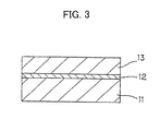
- FIG. 3 shows a conventional semiconductor layer.
- This semiconductor layer includes an Al 2 O 3 substrate 11 made of Al 2 O 3 , an AlN layer 12 which is formed on a surface of the Al 2 O 3 substrate 11, and a GaN growth layer 13 which is formed on the AlN layer 12 through epitaxial growth by utilizing an MOCVD (Metal Organic Chemical Vapor Deposition) method (refer to JP 52-36117 B for example).
- MOCVD Metal Organic Chemical Vapor Deposition
- the AlN layer 12 is formed between the Al 2 O 3 substrate 11 and the GaN growth layer 13, whereby mismatch in lattice constants can be reduced to reduce imperfect crystalline.
- the lattice constants of the AlN layer 12 and the GaN growth layer 13 cannot be perfectly made match each other, and thus it is difficult to further enhance crystal quality of the GaN growth layer 13.
- the conventional semiconductor layer is applied to a light emitting element, crystalline of a luminous layer is degraded, and luminous efficiency is reduced.
- an object of the present invention is to provide a semiconductor layer in which a GaN system epitaxial layer having high crystal quality can be obtained.
- the present invention provides a semiconductor layer characterized by including a first layer made of a Ga 2 O 3 system semiconductor, and a second layer obtained by replacing a part or all of oxygen atoms of the first layer with nitrogen atoms.
- the second layer which is obtained by replacing a part or all of the oxygen atoms of the first layer with the nitrogen atoms is formed on the first layer made of the Ga 2 O 3 system semiconductor, whereby the second layer made of the GaN system compound semiconductor having high crystalline is obtained without interposing a buffer layer.
- This embodiment mode is constituted by a first layer which is made of a Ga 2 O 3 system semiconductor, a second layer which is made of a GaN system compound semiconductor and which is obtained on the first layer by subjecting a surface of the first layer to nitriding processing or the like to replace a part or all of oxygen atoms of the first layer with nitrogen atoms, and a third layer which is made of a GaN system epitaxial layer on the second layer.
- the Ga 2 O 3 system semiconductor contains semiconductors such as Ga 2 O 3 , (In x Ga 1-x ) 2 O 3 where 0 ⁇ x ⁇ 1, (Al x Ga 1-x ) 2 O 3 where 0 ⁇ x ⁇ 1, and (In x Al y Ga 1-x-y ) 2 O 3 where 0 ⁇ x ⁇ 1, 0 ⁇ y ⁇ 1, and 0 ⁇ x + y ⁇ 1, and also contains semiconductors each showing an n-type conductive property or a p-type conductive property through atom replacement or atom defects made for such a semiconductor.
- the GaN system compound semiconductor and "the GaN system epitaxial layer” contain semiconductors such as GaN, In z Ga 1-z N where 0 ⁇ z ⁇ 1, Al z Ga 1-z N where 0 ⁇ z ⁇ 1, and In z Al p Ga 1-z-p N where 0 ⁇ z ⁇ 1, 0 ⁇ p ⁇ 1, and 0 ⁇ z + p ⁇ 1, and also contain semiconductors each showing an n-type conductive property or a p-type conductive property through atom replacement or atom defects made for such a semiconductor.
- the second layer and the third layer can be made of the same compound semiconductor as in the first layer made of Ga 2 O 3 , the second layer made of GaN, and the third layer made of GaN.
- the second layer and the third layer can also be made of different compound semiconductors, respectively, as in the first layer made of made of Ga 2 O 3 , the second layer made of GaN, and the third layer made of In z Ga 1-z N where 0 ⁇ z ⁇ 1.
- the second layer and the third layer can also be made of different compound semiconductors, respectively, and the first layer and the second layer can also be made in accordance with a combination different from that in the first example and the second example as in the first layer made of (In x Ga 1-x ) z O 3 where 0 ⁇ x ⁇ 1, the second layer made of Ir z Al p Ga 1-z-p N where 0 ⁇ z ⁇ 1, 0 ⁇ p ⁇ 1, and 0 ⁇ z + p ⁇ 1, and the third layer made of Al z Ga 1-z N where 0 ⁇ z ⁇ 1.
- the GaN system epitaxial layer having high crystal quality is obtained.
- FIG. 1 shows a semiconductor layer according to Embodiment 1 of the present invention.
- the semiconductor layer of Embodiment 1 includes a ⁇ -Ga 2 O 3 substrate 1, as a first layer, which is made of a ⁇ -Ga 2 O 3 single crystal, a GaN layer 2 with about 2 nm thickness, as a second layer, which is formed by subjecting a surface of the ⁇ -Ga 2 O 3 substrate 1 to nitriding processing, and a GaN growth layer 3, as a third layer, which is formed on the GaN layer 2 through epitaxial growth by utilizing an MOCVD method for example.
- Oxygen atoms of the ⁇ -Ga 2 O 3 substrate 1 are replaced with nitrogen atoms in the nitriding processing, thereby forming the GaN layer 2 .
- FIG. 2 shows processes for manufacturing the semiconductor layer.
- the ⁇ -Ga203 substrate 1 is manufactured by utilizing an FZ (floating zone) method (process a).
- FZ floating zone
- a ⁇ -Ga 2 O 3 seed crystal and a ⁇ -Ga 2 O 3 polycrystalline raw material are prepared.
- the ⁇ -Ga 2 O 3 seed crystal is obtained by cutting down a ⁇ -Ga 2 O 3 single crystal through utilization or the like of a cleaved face and has a prismatic shape having a square in cross section, and its axis direction matches a-axis ⁇ 100> orientation, b-axis ⁇ 010> orientation, or c-axis ⁇ 001> orientation.
- powders of Ga 2 O 3 with a purity of 4N are filled in a rubber tube, subjected to cold compression at 500 MPa, and sintered at 1500°C for 10 hours, thereby obtaining the ⁇ -Ga 2 O 3 polycrystalline raw material.
- heads of the ⁇ -Ga 2 O 3 seed crystal and the ⁇ -Ga 2 O 3 polycrystalline are made contact each other in ambient of mixed gas of nitrogen and oxygen (changing from 100% nitrogen to 100% oxygen) at a total pressure of 1 to 2 atmospheres in a silica tube, contact portions thereof are heated to be molten, and the dissolved matter of the ⁇ -Ga 2 O 3 polycrystalline is cooled, thereby producing the ⁇ -Ga 2 G 3 single crystal.
- the ⁇ -Ga 2 O 3 single crystal When being grown as a crystal in the b-axis ⁇ 010> orientation, the ⁇ -Ga 2 O 3 single crystal has strong cleavage in a (100) face, and hence the ⁇ -Ga 2 O 3 single crystal is cut along a face vertical to a face parallel to the (100) face, thereby manufacturing the ⁇ -Ga 2 O 3 substrate 1.
- the ⁇ -Ga 2 O 3 single crystal when being grown as a crystal in the ⁇ -axis ⁇ 100> orientation or c-axis ⁇ 001> orientation, the ⁇ -Ga 2 O 3 single crystal has weak cleavage in the (100) face and a (001) face. Hence, the processability for all the faces becomes excellent, and thus there is no limit to the cut face as described above.
- the ⁇ -Ga 2 O 3 substrate 1 is etched by being boiled in a nitric acid solution at 60°C (process b).
- the resulting ⁇ -Ga 2 O 3 substrate 1 is then immersed in ethanol and subjected to ultrasonic cleaning (process c).
- the ⁇ -Ga 2 O 3 substrate 1 is dried (process e) and subjected to vacuum cleaning at 1000°C in a growth chamber of an MOCVD system (process f) to clean a surface of the ⁇ -Ga 2 O 3 substrate 1.
- the ⁇ -Ga 2 O 3 substrate 1 is subjected to nitriding processing (process g). That is to say, the ⁇ -Ga 2 O 3 substrate 1 is heated for a predetermined period of time in a predetermined ambient atmosphere in the growth chamber of the MOCVD system.
- the ambient atmosphere including the atmosphere
- the heating temperature, and the heating period of time are suitably selected, whereby the desired GaN layer 2 is obtained on the surface of the ⁇ -Ga 2 O 3 substrate 1 .
- the ⁇ -Ga 2 O 3 substrate 1 is heated at 1050°C for 5 minutes in NH 3 ambient at 300 torr, whereby the thin GaN layer 2 with about 2 nm thickness is formed on the surface of the ⁇ -Ga 2 C 3 substrate 1.
- GaN is grown by utilizing the MOCVD method to obtain the GaN growth layer 3 (process h). That is to say, when a pressure in the growth chamber of the MOCVD system is reduced to 100 torr, and ammonia gas and trimethylgallium (TMG) are supplied as an N supply raw material and a Ga supply raw material to the growth chamber, respectively, the GaN growth layer 3 with about 100 nm thickness for example grows on the GaN layer 2 .
- the thickness of the GaN growth layer can be controlled by adjusting a concentration of the supply raw materials, the heating temperature, and the like.
- Embodiment 1 when trimethylaluminum (TMA) is supplied together with TMG, an AlGaN layer can be formed as the second layer instead of the GaN layer 2 .
- TMA trimethylaluminum
- TMI trimethylindium
- an InGaN layer can be formed as the second layer instead of the GaN layer 2 .
- InGaN, AlGaN or InGaAlN may also be grown instead of the GaN growth layer 3 .
- the lattice constants thereof can be made nealy match those of the GaN layer 2 .
- InAlGaN the lattice constants thereof can be made match those of the GaN layer 2 .
- a double hetero type light emitting element is obtained.
- a well layer and a barrier layer which are different in In composition ratio from each other are alternately formed for formation of the non-doped InGaN layer, a laser diode element having an MQW (multi-quantum well layer) is obtained.
- the GaN layer 2 and the substrate 1 are removed after the GaN growth layer 3 with a predetermined thickness grows, the GaN substrate is obtained.
- an InGaN layer, an AlGaN layer or an InGaAlN layer is formed instead of the GaN growth layer 3 , whereby respective substrates can be obtained.
- any other suitable growth method such as an EFG (Edge-defined Film-fed Growth method) method may also be adopted.
- EFG Erge-defined Film-fed Growth method
- MOCVD Metal Organic Chemical Vapor Deposition
- the semiconductor layer of the present invention is not limited to the light emitting element, and thus can be applied to various kinds of semiconductor components or parts.
- the second layer which is obtained by replacing a part or all of the oxygen atoms of the first layer with the nitrogen atoms is formed on the first layer made of the ⁇ -Ga 2 O 3 system semiconductor, whereby the second layer which is made of the GaN system compound semiconductor and which has the high crystalline is obtained without interposing a buffer layer.
- the lattice constants of the second layer and the GaN system epitaxial layer can be made match each other, or can be made exceedingly approximate to each other, and thus the GaN system epitaxial layer having the high crystal quality is obtained.
Landscapes
- Chemical & Material Sciences (AREA)
- Chemical Kinetics & Catalysis (AREA)
- General Chemical & Material Sciences (AREA)
- Engineering & Computer Science (AREA)
- Crystallography & Structural Chemistry (AREA)
- Materials Engineering (AREA)
- Metallurgy (AREA)
- Organic Chemistry (AREA)
- Led Devices (AREA)
- Crystals, And After-Treatments Of Crystals (AREA)
- Recrystallisation Techniques (AREA)
- Chemical Vapour Deposition (AREA)
Applications Claiming Priority (2)
| Application Number | Priority Date | Filing Date | Title |
|---|---|---|---|
| JP2003290862A JP4754164B2 (ja) | 2003-08-08 | 2003-08-08 | 半導体層 |
| EP04771516A EP1653502A4 (de) | 2003-08-08 | 2004-08-04 | Halbleiterschicht |
Related Parent Applications (1)
| Application Number | Title | Priority Date | Filing Date |
|---|---|---|---|
| EP04771516.4 Division | 2004-08-04 |
Publications (2)
| Publication Number | Publication Date |
|---|---|
| EP2472567A2 true EP2472567A2 (de) | 2012-07-04 |
| EP2472567A3 EP2472567A3 (de) | 2012-08-15 |
Family
ID=34131611
Family Applications (2)
| Application Number | Title | Priority Date | Filing Date |
|---|---|---|---|
| EP04771516A Ceased EP1653502A4 (de) | 2003-08-08 | 2004-08-04 | Halbleiterschicht |
| EP12162023A Ceased EP2472567A3 (de) | 2003-08-08 | 2004-08-04 | Halbleiterschicht |
Family Applications Before (1)
| Application Number | Title | Priority Date | Filing Date |
|---|---|---|---|
| EP04771516A Ceased EP1653502A4 (de) | 2003-08-08 | 2004-08-04 | Halbleiterschicht |
Country Status (7)
| Country | Link |
|---|---|
| US (2) | US7977673B2 (de) |
| EP (2) | EP1653502A4 (de) |
| JP (1) | JP4754164B2 (de) |
| KR (2) | KR101132546B1 (de) |
| CN (2) | CN101257079B (de) |
| TW (2) | TWI362365B (de) |
| WO (1) | WO2005015617A1 (de) |
Families Citing this family (29)
| Publication number | Priority date | Publication date | Assignee | Title |
|---|---|---|---|---|
| KR100482511B1 (ko) * | 2004-02-05 | 2005-04-14 | 에피밸리 주식회사 | Ⅲ-질화물계 반도체 발광소자 |
| JP4476691B2 (ja) * | 2004-05-13 | 2010-06-09 | 日本軽金属株式会社 | 酸化ガリウム単結晶複合体及びその製造方法並びに酸化ガリウム単結晶複合体を用いた窒化物半導体膜の製造方法 |
| JP2006237556A (ja) * | 2005-01-31 | 2006-09-07 | Kanagawa Acad Of Sci & Technol | GaN膜生成方法及び半導体素子並びにIII族窒化物の薄膜生成方法及びIII族窒化物の薄膜を有する半導体素子 |
| JP2006273684A (ja) * | 2005-03-30 | 2006-10-12 | Koha Co Ltd | Iii族酸化物系単結晶の製造方法 |
| JP5159040B2 (ja) | 2005-03-31 | 2013-03-06 | 株式会社光波 | 低温成長バッファ層の形成方法および発光素子の製造方法 |
| KR100691159B1 (ko) * | 2005-04-30 | 2007-03-09 | 삼성전기주식회사 | 질화갈륨계 반도체의 제조 방법 |
| JP4611103B2 (ja) * | 2005-05-09 | 2011-01-12 | 株式会社光波 | β−Ga2O3結晶の製造方法 |
| JP5180430B2 (ja) * | 2005-08-04 | 2013-04-10 | 独立行政法人物質・材料研究機構 | 発光素子 |
| JP2007254174A (ja) * | 2006-03-20 | 2007-10-04 | Nippon Light Metal Co Ltd | 酸化ガリウム単結晶及びその製造方法、並びに窒化物半導体用基板及びその製造方法 |
| JP2008156141A (ja) * | 2006-12-21 | 2008-07-10 | Koha Co Ltd | 半導体基板及びその製造方法 |
| KR101020958B1 (ko) * | 2008-11-17 | 2011-03-09 | 엘지이노텍 주식회사 | 산화갈륨기판 제조방법, 발광소자 및 발광소자 제조방법 |
| JP5529420B2 (ja) * | 2009-02-09 | 2014-06-25 | 住友電気工業株式会社 | エピタキシャルウエハ、窒化ガリウム系半導体デバイスを作製する方法、窒化ガリウム系半導体デバイス、及び酸化ガリウムウエハ |
| KR101047652B1 (ko) | 2009-12-18 | 2011-07-07 | 엘지이노텍 주식회사 | 발광소자 및 그 제조방법 |
| US9461124B2 (en) * | 2011-09-08 | 2016-10-04 | Tamura Corporation | Ga2O3 semiconductor element |
| JP5777479B2 (ja) * | 2011-10-14 | 2015-09-09 | 株式会社タムラ製作所 | β−Ga2O3系基板の製造方法、及び結晶積層構造体の製造方法 |
| US9966439B2 (en) * | 2013-07-09 | 2018-05-08 | Flosfia Inc. | Semiconductor device and manufacturing method for same, crystal, and manufacturing method for same |
| CN103456603B (zh) * | 2013-09-05 | 2016-04-13 | 大连理工大学 | 在镓系异质半导体衬底上制备氧化镓膜的方法及氧化镓膜 |
| KR102086360B1 (ko) * | 2013-11-07 | 2020-03-09 | 삼성전자주식회사 | n형 질화물 반도체의 전극형성방법, 질화물 반도체 소자 및 그 제조방법 |
| JP6248359B2 (ja) * | 2013-12-20 | 2017-12-20 | 住友電工デバイス・イノベーション株式会社 | 半導体層の表面処理方法 |
| CN104805505A (zh) * | 2014-01-24 | 2015-07-29 | 泉州市博泰半导体科技有限公司 | 一种制备目标薄膜层的方法 |
| JP2014123765A (ja) * | 2014-02-27 | 2014-07-03 | Sumitomo Electric Ind Ltd | ウエハ生産物、窒化ガリウム系半導体光素子 |
| TWI596710B (zh) | 2015-06-12 | 2017-08-21 | 國立交通大學 | 半導體元件的製備方法 |
| US10593544B2 (en) | 2016-10-14 | 2020-03-17 | Case Westen Reverse University | Method for forming a thin film comprising an ultrawide bandgap oxide semiconductor |
| GB201705755D0 (en) | 2017-04-10 | 2017-05-24 | Norwegian Univ Of Science And Tech (Ntnu) | Nanostructure |
| CN107587190A (zh) * | 2017-08-14 | 2018-01-16 | 南京大学 | 一种制备GaN衬底材料的方法 |
| CN107611004B (zh) * | 2017-08-14 | 2020-01-31 | 南京大学 | 一种制备自支撑GaN衬底材料的方法 |
| CN107833945B (zh) * | 2017-11-24 | 2019-09-24 | 中国科学院半导体研究所 | GaN基垂直LED结构及其制备方法 |
| CN116314278B (zh) * | 2023-05-22 | 2023-08-15 | 江西兆驰半导体有限公司 | 高电子迁移率晶体管外延结构及制备方法、hemt器件 |
| CN116885066B (zh) * | 2023-09-04 | 2023-12-01 | 江西兆驰半导体有限公司 | 发光二极管外延片及其制备方法、发光二极管 |
Citations (2)
| Publication number | Priority date | Publication date | Assignee | Title |
|---|---|---|---|---|
| JPS5236117B1 (de) | 1970-06-22 | 1977-09-13 | ||
| JP2003290862A (ja) | 2002-03-29 | 2003-10-14 | Tsukiboshi Seisakusho:Kk | 頭付部品の製造方法及びその装置 |
Family Cites Families (13)
| Publication number | Priority date | Publication date | Assignee | Title |
|---|---|---|---|---|
| US5777350A (en) * | 1994-12-02 | 1998-07-07 | Nichia Chemical Industries, Ltd. | Nitride semiconductor light-emitting device |
| JP4018177B2 (ja) | 1996-09-06 | 2007-12-05 | 株式会社東芝 | 窒化ガリウム系化合物半導体発光素子 |
| US6218207B1 (en) * | 1998-05-29 | 2001-04-17 | Mitsushita Electronics Corporation | Method for growing nitride semiconductor crystals, nitride semiconductor device, and method for fabricating the same |
| US6218280B1 (en) * | 1998-06-18 | 2001-04-17 | University Of Florida | Method and apparatus for producing group-III nitrides |
| JP4174913B2 (ja) * | 1999-06-04 | 2008-11-05 | 昭和電工株式会社 | Iii族窒化物半導体発光素子 |
| JP4083396B2 (ja) * | 2000-07-10 | 2008-04-30 | 独立行政法人科学技術振興機構 | 紫外透明導電膜とその製造方法 |
| JP2002029713A (ja) * | 2000-07-21 | 2002-01-29 | Tokai Univ | 窒化ガリウムの製造方法 |
| JP2002075986A (ja) * | 2000-08-30 | 2002-03-15 | Oki Electric Ind Co Ltd | GaAs系基板の表面処理方法 |
| JP4291527B2 (ja) * | 2000-10-13 | 2009-07-08 | 日本碍子株式会社 | Iii族窒化物エピタキシャル基板の使用方法 |
| JP3639789B2 (ja) * | 2001-01-31 | 2005-04-20 | シャープ株式会社 | 窒化物系半導体発光素子 |
| JP4187422B2 (ja) * | 2001-03-14 | 2008-11-26 | 明彦 吉川 | 半導体薄膜の形成方法およびその方法を用いて製造された半導体薄膜付き基板およびその半導体薄膜付き基板を用いた半導体デバイス。 |
| JP4431933B2 (ja) * | 2001-07-31 | 2010-03-17 | 信越半導体株式会社 | 発光素子の製造方法及び発光素子 |
| JP3679097B2 (ja) * | 2002-05-31 | 2005-08-03 | 株式会社光波 | 発光素子 |
-
2003
- 2003-08-08 JP JP2003290862A patent/JP4754164B2/ja not_active Expired - Fee Related
-
2004
- 2004-08-04 US US10/567,369 patent/US7977673B2/en not_active Expired - Fee Related
- 2004-08-04 CN CN2008100893858A patent/CN101257079B/zh not_active Expired - Fee Related
- 2004-08-04 WO PCT/JP2004/011531 patent/WO2005015617A1/ja not_active Ceased
- 2004-08-04 EP EP04771516A patent/EP1653502A4/de not_active Ceased
- 2004-08-04 KR KR1020067002599A patent/KR101132546B1/ko not_active Expired - Fee Related
- 2004-08-04 KR KR1020117030584A patent/KR101197416B1/ko not_active Expired - Fee Related
- 2004-08-04 EP EP12162023A patent/EP2472567A3/de not_active Ceased
- 2004-08-04 CN CNB2004800226892A patent/CN100394549C/zh not_active Expired - Fee Related
- 2004-08-06 TW TW093123606A patent/TWI362365B/zh not_active IP Right Cessation
- 2004-08-06 TW TW100134374A patent/TWI488814B/zh not_active IP Right Cessation
-
2011
- 2011-06-22 US US13/067,726 patent/US8674399B2/en not_active Expired - Fee Related
Patent Citations (2)
| Publication number | Priority date | Publication date | Assignee | Title |
|---|---|---|---|---|
| JPS5236117B1 (de) | 1970-06-22 | 1977-09-13 | ||
| JP2003290862A (ja) | 2002-03-29 | 2003-10-14 | Tsukiboshi Seisakusho:Kk | 頭付部品の製造方法及びその装置 |
Also Published As
| Publication number | Publication date |
|---|---|
| KR20060034723A (ko) | 2006-04-24 |
| CN101257079A (zh) | 2008-09-03 |
| KR101132546B1 (ko) | 2012-04-03 |
| JP2005064153A (ja) | 2005-03-10 |
| TW201213239A (en) | 2012-04-01 |
| US8674399B2 (en) | 2014-03-18 |
| WO2005015617A1 (ja) | 2005-02-17 |
| TWI488814B (zh) | 2015-06-21 |
| EP1653502A4 (de) | 2009-12-16 |
| US20110253973A1 (en) | 2011-10-20 |
| US7977673B2 (en) | 2011-07-12 |
| KR20120003506A (ko) | 2012-01-10 |
| TWI362365B (en) | 2012-04-21 |
| TW200510252A (en) | 2005-03-16 |
| CN100394549C (zh) | 2008-06-11 |
| JP4754164B2 (ja) | 2011-08-24 |
| EP2472567A3 (de) | 2012-08-15 |
| CN101257079B (zh) | 2012-07-18 |
| KR101197416B1 (ko) | 2012-11-05 |
| US20060289860A1 (en) | 2006-12-28 |
| CN1833310A (zh) | 2006-09-13 |
| EP1653502A1 (de) | 2006-05-03 |
Similar Documents
| Publication | Publication Date | Title |
|---|---|---|
| US8674399B2 (en) | Semiconductor layer | |
| US7955957B2 (en) | Group III-nitride semiconductor thin film, method for fabricating the same, and group III-nitride semiconductor light emitting device | |
| US20060225643A1 (en) | AlGaN substrate and production method thereof | |
| US7935955B2 (en) | Group III nitride semiconductor multilayer structure | |
| KR100583163B1 (ko) | 질화물 반도체 및 그 제조방법 | |
| JP2008156141A (ja) | 半導体基板及びその製造方法 | |
| JPH11135889A (ja) | 結晶成長用基板及びそれを用いた発光装置 | |
| KR100841269B1 (ko) | Ⅲ족 질화물 반도체 다층구조물 | |
| KR20130035995A (ko) | 구조체, 및 반도체 기판의 제조 방법 | |
| KR101008856B1 (ko) | Ⅲ족 질화물 반도체 소자의 제조방법 | |
| JP3987879B2 (ja) | 窒化物半導体発光素子とその製造方法 | |
| KR100765386B1 (ko) | 질화 갈륨계 화합물 반도체 및 이의 제조 방법 | |
| JPH09169599A (ja) | 窒化ガリウム系化合物半導体の製造方法 | |
| WO2007078065A1 (en) | Gallium nitride-based compound semiconductor | |
| JP2006032737A (ja) | 発光素子 |
Legal Events
| Date | Code | Title | Description |
|---|---|---|---|
| 17P | Request for examination filed |
Effective date: 20120329 |
|
| AC | Divisional application: reference to earlier application |
Ref document number: 1653502 Country of ref document: EP Kind code of ref document: P |
|
| AK | Designated contracting states |
Kind code of ref document: A2 Designated state(s): AT BE BG CH CY CZ DE DK EE ES FI FR GB GR HU IE IT LI LU MC NL PL PT RO SE SI SK TR |
|
| PUAI | Public reference made under article 153(3) epc to a published international application that has entered the european phase |
Free format text: ORIGINAL CODE: 0009012 |
|
| PUAL | Search report despatched |
Free format text: ORIGINAL CODE: 0009013 |
|
| AK | Designated contracting states |
Kind code of ref document: A3 Designated state(s): AT BE BG CH CY CZ DE DK EE ES FI FR GB GR HU IE IT LI LU MC NL PL PT RO SE SI SK TR |
|
| RIC1 | Information provided on ipc code assigned before grant |
Ipc: H01L 33/00 20100101ALI20120709BHEP Ipc: H01L 21/20 20060101AFI20120709BHEP Ipc: H01L 21/02 20060101ALI20120709BHEP Ipc: C30B 25/02 20060101ALI20120709BHEP Ipc: C30B 25/20 20060101ALI20120709BHEP Ipc: H01S 5/343 20060101ALI20120709BHEP Ipc: C23C 16/34 20060101ALI20120709BHEP |
|
| RIN1 | Information on inventor provided before grant (corrected) |
Inventor name: GARCIA VILLORA, ENCARNACION ANTONIA Inventor name: SHIMAMURA, KIYOSHI Inventor name: AOKI, KAZUO Inventor name: ICHINOSE, NOBORU |
|
| 17Q | First examination report despatched |
Effective date: 20140526 |
|
| STAA | Information on the status of an ep patent application or granted ep patent |
Free format text: STATUS: THE APPLICATION HAS BEEN REFUSED |
|
| 18R | Application refused |
Effective date: 20150919 |