EP2472580A2 - Capteur incurvé formé à partir de fibres en silicone et son procédé de fabrication - Google Patents
Capteur incurvé formé à partir de fibres en silicone et son procédé de fabrication Download PDFInfo
- Publication number
- EP2472580A2 EP2472580A2 EP11006759A EP11006759A EP2472580A2 EP 2472580 A2 EP2472580 A2 EP 2472580A2 EP 11006759 A EP11006759 A EP 11006759A EP 11006759 A EP11006759 A EP 11006759A EP 2472580 A2 EP2472580 A2 EP 2472580A2
- Authority
- EP
- European Patent Office
- Prior art keywords
- sensor
- image
- sensors
- light transmissive
- curved
- Prior art date
- Legal status (The legal status is an assumption and is not a legal conclusion. Google has not performed a legal analysis and makes no representation as to the accuracy of the status listed.)
- Granted
Links
Images
















Classifications
-
- H—ELECTRICITY
- H10—SEMICONDUCTOR DEVICES; ELECTRIC SOLID-STATE DEVICES NOT OTHERWISE PROVIDED FOR
- H10F—INORGANIC SEMICONDUCTOR DEVICES SENSITIVE TO INFRARED RADIATION, LIGHT, ELECTROMAGNETIC RADIATION OF SHORTER WAVELENGTH OR CORPUSCULAR RADIATION
- H10F39/00—Integrated devices, or assemblies of multiple devices, comprising at least one element covered by group H10F30/00, e.g. radiation detectors comprising photodiode arrays
- H10F39/80—Constructional details of image sensors
- H10F39/802—Geometry or disposition of elements in pixels, e.g. address-lines or gate electrodes
- H10F39/8023—Disposition of the elements in pixels, e.g. smaller elements in the centre of the imager compared to larger elements at the periphery
-
- H—ELECTRICITY
- H04—ELECTRIC COMMUNICATION TECHNIQUE
- H04N—PICTORIAL COMMUNICATION, e.g. TELEVISION
- H04N25/00—Circuitry of solid-state image sensors [SSIS]; Control thereof
- H04N25/60—Noise processing, e.g. detecting, correcting, reducing or removing noise
-
- H—ELECTRICITY
- H04—ELECTRIC COMMUNICATION TECHNIQUE
- H04N—PICTORIAL COMMUNICATION, e.g. TELEVISION
- H04N25/00—Circuitry of solid-state image sensors [SSIS]; Control thereof
- H04N25/70—SSIS architectures; Circuits associated therewith
- H04N25/702—SSIS architectures characterised by non-identical, non-equidistant or non-planar pixel layout
-
- H—ELECTRICITY
- H10—SEMICONDUCTOR DEVICES; ELECTRIC SOLID-STATE DEVICES NOT OTHERWISE PROVIDED FOR
- H10F—INORGANIC SEMICONDUCTOR DEVICES SENSITIVE TO INFRARED RADIATION, LIGHT, ELECTROMAGNETIC RADIATION OF SHORTER WAVELENGTH OR CORPUSCULAR RADIATION
- H10F39/00—Integrated devices, or assemblies of multiple devices, comprising at least one element covered by group H10F30/00, e.g. radiation detectors comprising photodiode arrays
- H10F39/011—Manufacture or treatment of image sensors covered by group H10F39/12
-
- H—ELECTRICITY
- H10—SEMICONDUCTOR DEVICES; ELECTRIC SOLID-STATE DEVICES NOT OTHERWISE PROVIDED FOR
- H10F—INORGANIC SEMICONDUCTOR DEVICES SENSITIVE TO INFRARED RADIATION, LIGHT, ELECTROMAGNETIC RADIATION OF SHORTER WAVELENGTH OR CORPUSCULAR RADIATION
- H10F39/00—Integrated devices, or assemblies of multiple devices, comprising at least one element covered by group H10F30/00, e.g. radiation detectors comprising photodiode arrays
- H10F39/80—Constructional details of image sensors
- H10F39/804—Containers or encapsulations
-
- H—ELECTRICITY
- H10—SEMICONDUCTOR DEVICES; ELECTRIC SOLID-STATE DEVICES NOT OTHERWISE PROVIDED FOR
- H10F—INORGANIC SEMICONDUCTOR DEVICES SENSITIVE TO INFRARED RADIATION, LIGHT, ELECTROMAGNETIC RADIATION OF SHORTER WAVELENGTH OR CORPUSCULAR RADIATION
- H10F39/00—Integrated devices, or assemblies of multiple devices, comprising at least one element covered by group H10F30/00, e.g. radiation detectors comprising photodiode arrays
- H10F39/80—Constructional details of image sensors
- H10F39/806—Optical elements or arrangements associated with the image sensors
-
- H—ELECTRICITY
- H10—SEMICONDUCTOR DEVICES; ELECTRIC SOLID-STATE DEVICES NOT OTHERWISE PROVIDED FOR
- H10F—INORGANIC SEMICONDUCTOR DEVICES SENSITIVE TO INFRARED RADIATION, LIGHT, ELECTROMAGNETIC RADIATION OF SHORTER WAVELENGTH OR CORPUSCULAR RADIATION
- H10F39/00—Integrated devices, or assemblies of multiple devices, comprising at least one element covered by group H10F30/00, e.g. radiation detectors comprising photodiode arrays
- H10F39/011—Manufacture or treatment of image sensors covered by group H10F39/12
- H10F39/024—Manufacture or treatment of image sensors covered by group H10F39/12 of coatings or optical elements
-
- H—ELECTRICITY
- H10—SEMICONDUCTOR DEVICES; ELECTRIC SOLID-STATE DEVICES NOT OTHERWISE PROVIDED FOR
- H10F—INORGANIC SEMICONDUCTOR DEVICES SENSITIVE TO INFRARED RADIATION, LIGHT, ELECTROMAGNETIC RADIATION OF SHORTER WAVELENGTH OR CORPUSCULAR RADIATION
- H10F39/00—Integrated devices, or assemblies of multiple devices, comprising at least one element covered by group H10F30/00, e.g. radiation detectors comprising photodiode arrays
- H10F39/80—Constructional details of image sensors
- H10F39/805—Coatings
- H10F39/8057—Optical shielding
Definitions
- the present invention relates to a curved concave sensor formed from silicon fibers.
- the rangefinder came first. It was followed by the SLR, or, single lens reflex and finally the Compact “Point and Shoot” cameras. Most portable cameras today use rangefinder, SLR or “Point and Shoot” formats.
- Figure 1 is a simplified view of a conventional camera, which includes an enclosure, an objective lens and a flat section of photographic film or a flat sensor.
- a simple lens with a flat film or sensor faces several problems. Light travels over a longer pathway to the edges of the film or the sensor's image area, diluting those rays. Besides being weaker, as those rays travel farther to the sensor's edges, they suffer more "rainbow effect," or chromatic aberration.
- Figure 2 presents a simplified view of the human eye, which includes a curved surface for forming an image.
- the human eye for example, needs only a cornea and a single lens to form an image. But on average, one human retina contains twenty-five million rods and six million cones.
- Today's high end cameras use lenses with from six to twenty elements. Only the rarest, most expensive cameras have as many pixels as the eye has rods and cones, and none of these cameras capture images after sunset without artificial light.
- the eagle's retina has eight times as many retinal sensors as the human eye. They are arranged on a sphere the size of a marble. The eagle's rounded sensors make simpler optics possible. No commercially available camera that is available today has a pixel count which equals a fourth of the count of sensors in an eagle's eye.
- the eagle eye uses a simple lens and a curved retina. The best conventional cameras use multiple element lenses with sophisticated coatings, rare earth materials and complex formulas. This is all to compensate for their flat sensors.
- the eagle sees clearly at noon, in daylight or at dusk with simpler, lighter and smaller optics than any camera.
- Rangefinder cameras are typified by a broad spectrum from the early LEICATM thirty-five millimeter cameras, for professionals, to the later "INSTAMATICTM” film types for the masses. (Most of KODAK'sTM INSTAMATICTM cameras did not focus, so they were not true rangefinders. A few "Instamatic type” models focused, and had a "viewing" lens separated from the "taking” lens, qualifying them as rangefinders.)
- Rangefinder cameras have a "taking" lens to put the image on the film (or sensor today) when the shutter opens and closes; mechanically or digitally. These cameras use a second lens for viewing the scene. Focusing takes place through this viewing lens which connects to, and focuses, the taking lens.
- the taking lens and the viewing lens are different, and have different perspectives on the scene being photographed, the taken image is always slightly different than the viewed image. This problem, called parallax, is minor in most situations but becomes acute at close distances.
- Some rangefinder cameras use a frame in the viewfinder which shifts the border to match that of the taking lens as the focus changes. This aligns the view with the picture actually taken, but only for that portion that's in focus. Backgrounds and foregrounds that are not in focus shift, so those parts of the photographed image still vary slightly from what was seen in the viewfinder.
- rangefinder cameras that use interchangeable or attachable lenses, but parallax remains an unsolvable problem and so no manufacturer has ever successfully marketed a rangefinder camera with much beyond slightly wide or mildly long telephoto accessories. Any added rangefinder lens must also be accompanied by a similar viewfinder lens. If not, what is viewed won't match the photograph taken at all. This doubles the lens cost.
- these lenses range from 18 mm “fisheye” lenses to 1,000 mm super-telephoto lenses, plus optical zooms that cover many ranges in between.
- SLR disadvantages are the complexity of the mechanism, requiring more moving parts than with other formats, plus the noise, vibration and delay caused by the mirror motion. Also, lens designs are constrained, due to the lens needing to be placed farther out in front of the path of the moving mirror, which is more distant from the film or sensor, causing lenses to be heavier, larger and less optimal. There is also the introduction of dust, humidity and other foreign objects into the camera body and on the rear lens elements when lenses are changed.
- SLRs need precise lens and body mounting mechanisms, which also have mechanical and often electrical connections between the SLR lens and the SLR body. This further adds weight, complexity and cost.
- Optical zoom lenses reduce the need to change lenses with an SLR. The photographer simply zooms in or out for most shots. Still, for some situations, an even wider or longer accessory lens is required with the SLR, and the photographer changes lenses anyway.
- the Gartner Group reported that over one billion mobile phones were sold worldwide in 2009. A large portion of currently available mobile phones include a camera. These cameras are usually low quality photographic devices with simple planar arrays situated behind a conventional lens. The quality of images that may be captured with these cell phone cameras is generally lower than that which may be captured with dedicated point-and-shoot or more advanced cameras. Cell phone cameras usually lack advanced controls for shutter speed, telephoto or other features.
- the present invention comprises methods and apparatus for a curved sensor which is manufactured from silicon or other fibers.
- pixels having varying sizes are formed on a sensor.
- every other pixel in each ring of pixels is positioned slightly above its two neighboring pixels.
- the present invention provides methods and apparatus related to a camera having a non-planar or curved sensor.
- the present invention may be incorporated in a mobile communication device.
- the terms "mobile communication device” and “mobile communication means” are intended to include any apparatus or combination of hardware and/or software which may be used to communicate, which includes transmitting and/or receiving information, data or content or any other form of signals or intelligence.
- mobile communication devices include cellular or wireless telephones, smart phones, personal digital assistants, laptop or netbook computers, iPadsTM or other readers/computers, or any other generally portable device which may be used for telecommunications or viewing or recording visual content.
- the present invention includes curved or otherwise non-planar sensors.
- the non-planar surfaces of the sensor used in the present invention comprise a plurality of small flat segments which altogether approximate a curved surface.
- the sensor used by the present invention occupies three dimensions of space, as opposed to conventional sensors, which are planes that are substantially and generally contained in two physical dimensions.
- the present invention may utilize sensors which are configured in a variety of three-dimensional shapes, including, but not limited to, spherical, paraboloidal and ellipsoidal surfaces.
- curvilinear and curved encompass any line, edge, boundary, segment, surface or feature that is not completely colinear with a straight line.
- sensor encompasses any detector, imaging device, measurement device, transducer, focal plane array, charge-coupled device (CCD), complementary metal-oxide semiconductor (CMOS) or photocell that responds to an incident photon of any wavelength.
- CCD charge-coupled device
- CMOS complementary metal-oxide semiconductor
- Embodiments of the present invention are configured to record images in the optical spectrum, other embodiments of the present invention may be used for a variety of tasks which pertain to gathering, sensing and/or recording other forms of radiation.
- Embodiments of the present invention include systems that gather and/or record color, black and white, infra-red, ultraviolet, x-rays or any other stream of radiation, emanation, wave or particle.
- Embodiments of the present invention also include systems that record still images or motion pictures.
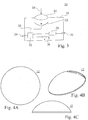
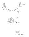
- Figure 3 provides a generalized schematic diagram of a digital camera 10 with a curved sensor 12 sub-assembly which may be incorporated into a mobile communication device.
- a housing 14 has an optical element 16 mounted on one of its walls.
- the objective lens 16 receives incoming light 18.
- the optical element is an objective lens.
- the sensor 12 converts the energy of the incoming photons 18 to an electrical output 20, which is then fed to a signal or photon processor 22.
- the signal processor 22 is connected to user controls 24, a battery or power supply 26 and to a solid state memory 28. Images created by the signal processor 22 are stored in the memory 28. Images may be extracted or downloaded from the camera through an output terminal 30, such as a USB port.
- Embodiments of the present invention include, but are not limited to, mobile communication devices with a camera that incorporate the following sensors:
- a flat center sensor might be surrounded by these "petals" with squared-off points.
- Figures 14A, 14B and 14C depict an alternative method for forming a curved sensor.
- Figure 14A depicts a dome-shaped first mandrel 43a on a substrate 43b.
- Figure 14B a thin sheet of heated deformable material 43c is impressed over the first mandrel 43a.
- the central area of the deformable material 43c takes the shape of the first mandrel 43a, forming a generally hemispherical base 43e for a curved sensor, as shown in Figure 14C .
- Figures 14D, 14E and 14F depict an alternative method for forming the base of a curved sensor.
- a second sheet of heated, deformable material 43f is placed over a second mandrel 43g.
- a vacuum pressure is applied to ports 43h, which draws the second sheet of heated, deformable material 43f downward into the empty region 43i enclosed by the second mandrel 43g.
- Figure 14E illustrates the next step in the process.
- a heater 43j increases the temperature of the second mandrel 43g, while the vacuum pressure imposed on ports 43h pulls the second sheet of heated, deformable material 43f down against the inside of the second mandrel 43g.
- Figure 14F shows the resulting generally hemispherical dome 43k, which is then used as the base of a curved sensor.
- Figure 14G shows a generally hemispherical base 43e or 43k for a curved sensor after sensor pixels 43l have been formed on the base 43e or 43k.
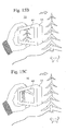
- Figure 15A shows a camera taking a wide angle photo.
- Figure 15A shows the same camera taking a normal perspective photo, while Figure 15B shows a telephoto view. In each view, the scene stays the same.
- the view screen on the camera shows a panorama in Figure 15A , a normal view in Figure 15B , and detail from the distance in Figure 15C .
- digital zoom shows the operator exactly the scene that is being processed from the camera sensor.
- Digital zoom is software-driven.
- the camera either captures only a small portion of the central image, the entire scene or any perspective in between.
- the monitor shows the operator what portion of the overall image is being recorded.
- the software can use all the data. Since the center has more pixels per area, the telephoto image, even though it is cropped down to a small section of the sensor, produces a crisp image. This is because the pixels are more dense at the center.
- the software can compress the data in the center to approximate the density of the pixels in the edges of the image. Because so many more pixels are involved in the center of this wide angle scene, this does not effect wide angle image quality. Yet, if uncompressed, the center pixels represent unnecessary and invisible detail captured, and require more storage capacity and processing time. Current photographic language might call the center section as being processed “RAW” or uncompressed when shooting telephoto but being processed as "JPEG” or other compression algorithm in the center when the image is wide angle.
- Digital zoom is currently disdained by industry experts. When traditional sensors capture an image, digital zooming creates images that break up into jagged lines, forms visible pixels and yields poor resolution.
- Optical zoom has never created images as sharp as fixed focus length lenses are capable of producing. Optical zooms are also slower, letting less light through the optical train.
- Embodiments of the present invention provide lighter, faster, cheaper and more dependable cameras.
- the present invention provides digital zoom. Since this does not require optical zoom, it uses inherently lighter lens designs with fewer elements.
- more pixels are concentrated in the center of the sensor, and fewer are placed at the edges of the sensor.
- Various densities may be arranged in between the center and the edges. This feature allows the user to zoom into a telephoto shot using the center section only, and still have high resolution.
- the center pixels when viewing the photograph in the wide field of view, are "binned" or summed together to normalize the resolution to the value of the outer pixel density.
- the center pixels When viewing the photograph in telephoto mode, the center pixels are utilized in their highest resolution, showing maximum detail without requiring any adjustment of lens or camera settings.
- the digital zoom feature offers extra wide angle to extreme telephoto zoom. This feature is enabled due to the extra resolving power, contrast, speed and color resolution lenses are able to deliver when the digital sensor is not flat, but curved, somewhat like the retina of a human eye.
- the average human eye, with a cornea and single lens element uses, on average, 25 million rods and 6 million cones to capture images. This is more image data than is captured by all but a rare and expensive model or two of the cameras that are commercially available today, and those cameras typically must use seven to twenty element lenses, since they are constrained by flat sensors. These cameras cannot capture twilight images without artificial lighting, or, by boosting the ISO which loses image detail.
- the center of the sensor, where the digitally zoomed telephoto images are captured is configured with dense pixilation, which enables higher quality digitally zoomed images.
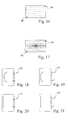
- Figures 16 and 17 illustrate this feature, which utilizes a high density concentration of pixels 48 at the center of a sensor. By concentrating pixels near the central region of the sensor, digital zoom becomes possible without loss of image detail.
- This unique approach provides benefits for either flat or curved sensors.
- a conventional sensor 46 is shown, which has pixels 48 that are generally uniformly disposed over the surface of the sensor 46.
- Figure 17 shows a sensor 50 produced in accordance with the present invention, which has pixels 48 that are more densely arranged toward the center of the sensor 50.
- suitable software compresses the dense data coming from the center of the image when the camera senses that a wide angle picture is being taken. This feature greatly reduces the processing and storage requirements for the system.
- inventions include a lens shade, which senses the image being captured, whether wide angle or telephoto.
- a lens shade which senses the image being captured, whether wide angle or telephoto.
- the camera senses a wide angle image, it retracts the shade, so that the shade does not get into the image area.
- it senses the image is telephoto, it extends, blocking extraneous light from the non-image areas, which can cause flare and fogged images.
- Figures 18 and 19 provide views of a camera equipped with an optional retractable lens shade.
- the lens shade is retracted, as indicated by reference character 52.
- the lens shade is extended, as indicated by reference character 54.
- Figures 20 and 21 provide similar views to Figures 18 and 19 , but of a camera with a planar sensor, indicating that the lens shade feature is applicable independently.
- Embodiments of the present invention reduce the dust problem that plagues conventional cameras since no optical zoom or lens changes are needed. Accordingly, the camera incorporated into the mobile communication device is sealed. No dust enters to interfere with image quality.
- An inert desiccated gas such as Argon, Xenon or Krypton may be sealed in the lens and sensor chambers within the enclosure 14, reducing oxidation and condensation. If these gases are used, the camera also gains benefits from their thermal insulating capability and temperature changes will be moderated, and the camera can operate over a wider range of temperatures.
- the entire camera may be sealed with an inert gas, such as Argon, Krypton or Xenon.
- an inert gas such as Argon, Krypton or Xenon.
- the present invention may be used in conjunction with a radically high speed lens, useable for both surveillance without flash (or without floods for motion) or fast action photography. This becomes possible again due to the non-planar sensor, and makes faster ranges like a f/0.7 or f/0.35 lens designs, and others, within practical reach, since the restraints posed by a flat sensor (or film) are now gone.
- an inert gas like Argon, Xenon or Krypton may be inserted, e.g.,injected during final assembly, reducing corrosion and rust.
- the camera can then operate in a wider range of temperatures. This is both a terrestrial benefit, and, is a huge advantage for cameras installed on satellites.
- Figures 22 and 23 illustrate a series of alternative sensor arrays with sensor segments 32c separated by gaps 34, to facilitate easier sensor assembly.
- a still camera which utilizes this sensor array takes two pictures in rapid succession.
- a first sensor array is shown in its original position 74, and is also shown in a rotated position 76.
- the position of the sensor arrays changes between the times the first and second pictures are taken.
- Software is used to recognize the images missing from the first exposure, and stitches that data in from the second exposure.
- the change in the sensor motion or direction shift may vary, depending on the pattern of the sensor facets.
- a motion camera can do the same, or, in a different embodiment, can simply move the sensor and capture only the new image using the data from the prior position to fill in the gaps in a continuous process.
- This method captures an image using a moveable sensor with gaps between the sensors in its array of sensors. This method makes fabricating much easier, because the spaces between segments become less critical. So, in one example, a square sensor in the center is surrounded by a row of eight more square sensors, which, in turn, is surrounded by another row of sixteen square sensors. The sensors are sized to fit the circular optical image, and each row curves in slightly more, creating the non-planar total sensor.
- the camera first takes one picture.
- the sensor immediately rotates or shifts slightly and a second image is immediately captured.
- Software can tell where the gaps were and stitches the new data from the second shot into the first. Or, depending on the sensor's array pattern, it may shift linearly in two dimensions, and possibly move in an arc in the third dimension to match the curve.
- the complex sensor in this case, is a large sensor comprising multiple smaller sensors.
- the gaps between each sensor lose data that is essential to make the complete image.
- Small gaps reduce the severity of this problem, but smaller gaps make the assembly of the sensor more difficult.
- Larger gaps make assembly easier and more economical, but, create an even less complete image.
- the present method solves that problem by moving the sensor after the first image, and taking a second image quickly. This gives the complete image and software can isolate the data that is collected by the second image that came from the gaps and splice it into the first image.
- the camera uses, but changes in a radical way, an industry technique known as "image stabilization.”
- image stabilization an industry technique known as "image stabilization.”
- the camera may use image stabilization in both the first and second images. This method neutralizes the effect of camera motion during an exposure. Such motion may come from hand tremors or engine vibrations.
- the camera will reverse image stabilization and introduce "image de-stabilization” or "intentional jitter” to move the image slightly over the sensor for the second exposure. This, with a sensor fixed in its position, also gives a shift to the second exposure so the gaps between the facets from the first exposure can be detected, and, the missing imagery recorded and spliced into the final image.
- the senor rotates back and forth.
- the sensor may shift sideways or diagonally.
- the sensor may also be rotated through some portion of arc of a full circle.
- the sensor might rotate continuously, while the software combines the data into a complete image.
- Figures 24A and 24B also shows a second set of sensors.
- the sensor is first shown in its original position 78, and is then shown in a displaced position 80.
- Figures 25A, 25B, 25C and 25D reveal four alternative grid patterns for four alternative embodiments of sensors 82, 84, 86 and 88.
- the gaps 34 between the facets 32e, 32f, 32g and 32h enable the manufacturing step of forming a curved sensor.
- Figures 26, 27 and 28 provide views of alternative embodiments of electrical connections to sensors.
- Figure 26 shows a sensor 90 has a generally spiral-shaped electrical connector 92.
- the conductor is connected to the sensor at the point identified by reference character 94, and is connected to a signal processor at the point identified by reference character 96.
- This embodiment of an electrical connection may be used when the sensor is rotated slightly between a first and second exposure, as illustrated in Figure 23 . This arrangement reduces the flexing of the conductor 92, extending its life.
- the processor may be built into the sensor assembly.
- Figure 27 shows the back of a sensor 102 with an "accordion" shape conductor 100, which is joined to the sensor at point A and to a processor at point B. This embodiment may be used when the sensor is shifted but not rotated between a first and second exposure, as illustrated in Figure 24 .
- This type of connection like the coiled wire connection, make an oscillating sensor connection durable.
- Figure 28 shows the back of a sensor 114 having generally radially extending conductors.
- the conductors each terminate in brush B which are able to contact a ring.
- the brushes move over and touch the ring, collecting an output from the rotating sensor, and then transmit the output to the processor at the center C.
- This embodiment may be used when the sensor is rotated between exposures.
- this connection makes another embodiment possible; a continuously rotating sensor. In that embodiment, the sensor rotates in one direction constantly.
- the software detects the gaps, and fills in the missing data from the prior exposure.
- Figure 29 offers a block diagram of a wireless connection 118.
- a sensor 12 is connected to a transmitter 120, which wirelessly sends signals to a receiver 122.
- the receiver is connected to a signal processor 124.
- the advantages offered by the present invention include, but are not limited to:
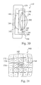
- a mobile communication device including a camera 150 having many of the preferred features of the present invention will now be described with reference to Figures 30 and 31 .
- the camera comprises an hermetically-sealed enclosure 154 accommodating a generally curved sensor 160 and a lens 156.
- Enclosure 154 is filled with Argon, Xenon or Krypton.
- a front view of the sensor 160 is illustrated schematically in Fig. 31 and comprises a plurality of flat square pixel elements or facets 162 arranged to be relatively inclined so as to form an overall curved configuration.
- the center square 170 is the largest, and the adjacent ring of eight squares 172 is made of slightly smaller squares so that they touch or nearly touch at their outermost corners.
- the next ring of sixteen squares 176 has slightly smaller squares than the inner ring 172.
- the center square 170 has the highest density of pixels; note that this square alone is used in the capture of telephoto images.
- the squares of inner ring 172 have medium density pixilation, which for normal photography gives reasonable definition.
- the outer ring 176 of sixteen squares has the least dense pixel count.
- the gaps 164 between the elements 162 are used as pathways for electrical connectors.
- the camera 150 further comprises a lens shade extender arrangement 180 comprising a fixed, inner shade member 182, first movable shade member 184 and a second, radially outermost, movable shade member 186.
- a lens shade extender arrangement 180 comprising a fixed, inner shade member 182, first movable shade member 184 and a second, radially outermost, movable shade member 186.
- the shade member 184 is extended so that stray light from outside of the viewing area is blocked. In this mode, a portion of the data facets 172 of the curved sensor are compressed. To reduce processing time and storage requirements, the data from the most center area 170, with higher density of pixels, can be normalized across the entire image field.
- shade member 186 When the user zooms out digitally to a telephoto perspective, shade member 186 is extended. In this mode, only the center portion 170 of the curved sensor 160 is used. Since only that sensor center is densely covered with pixels, the image definition will be crisp.
- camera 150 uses two exposures to fill in any gaps within the sensors range, i.e., to obtain the pixel data missing from a single exposure due to the presence of gaps 164.
- the camera deploys one of two methods. In the first, as previously described, the sensor moves and a second exposure is taken in rapid succession.
- the processing software detects the image data that was missed in the first exposure, due to the sensor's gaps, and "stitches" that missing data into the first exposure. This creates a complete image.
- the process is run continuously for motion pictures, with the third exposure selecting missing data from either the preceding or the following exposure, again to create a complete image.
- the dashed lines shown in Figure 30 indicate the two-dimensional motion of the lens for one embodiment of the focusing process.
- the lens does not move back and forth, but, rather, tilts to alter the position of the image on the sensor.
- the above-described camera 150 has numerous advantages.
- the sealing of the enclosure 154 with a gas like argon prevents oxidation of the parts and provides thermal insulation for operation throughout a broader range of temperature.
- the center square 170 with a high pixel density which is relatively more expensive, it is also relatively small, and it is only necessary to provide a single such square, this keeping down the overall cost.
- a huge cost advantage is that it provides an acceptable digital zoom without the need for accessory lenses. Accessory lenses cost far, far more than this sensor, and are big, heavy and slow.
- the outer ring 176 has the smallest squares and the lowest pixel count and so they are relatively inexpensive. Thus, taking into account the entire assembly of squares, the total cost of the sensor is low, bearing in mind it is capable of providing an acceptable performance over a wide range of perspectives.
- lens 156 may comprise a plurality of elements.
- the enclosure 154 is sealed with another inert gas, or a non-reactive gas such as Nitrogen, Krypton, Xenon or Argon; or it may not be sealed at all.
- a non-reactive gas such as Nitrogen, Krypton, Xenon or Argon
- the pixels or facets 170, 172, 176 may be rectangular, hexagonal or of any other suitable shape. Although a central pixel and two surrounding "square rings" of pixels are described, the sensor may comprise any desired number of rings.
- FIG 32 there is shown a block diagram of a camera 250 having many of the features of the camera 150 of Figures 30 and 31 .
- a non-planar sensor 260 has a central region 270 with high pixel density and a surrounding region comprising facets 272 with low pixel density.
- a shutter control 274 is also illustrated. The shutter control 274 together with a focus/stabilization actuating mechanism 290 for lens 256 and a lens shade actuator 280 are controlled by an image sequence processor 200.
- the signals from pixels in facets 270, 272 are supplied to a raw sensor capture device 202.
- An output of device 202 is connected to a device 204 for effecting auto focus, auto exposure/gain and auto white balance.
- Another output of device 202 is supplied to a device 206 for effecting pixel density normalization, the output of which is supplied to an image processing engine 208.
- a first output of engine 208 is supplied to a display/LCD controller 210.
- a second output of engine 208 is supplied to a compression and storage controller 212.
- Figures 33 , 34, 35 and 36 present views of one embodiment of the invention, which combines a curved sensor camera with a mobile communication device.
- the device may be a cellular telephone; laptop, notebook or netbook computer; or any other appropriate device or means for communication, recordation or computation.
- Figure 33 shows a side view 300 of one particular embodiment of the device, which includes an enhanced camera 150 for still photographs and video on both the front 305a and the back 305b sides.
- a housing 302 encloses a micro-controller 304, a display screen 306, a touch screen interface 308a and a user interface 308b.
- a terminal for power and/or data 310, as well as a microphone, are located near the bottom of the housing 302.
- a volume and/or mute control switch 318 is mounted on one of the slender sides of the housing 302.
- a speaker 314 and an antenna 315 reside inside the upper portion of the housing 302.
- Figures 34 and 35 offer perspective views 330 and 334 of an alternative embodiment 300a.
- Figures 36 and 37 offer perspective views 338 and 340 of yet another alternative embodiment 300b.
- This alternative method uses multiple rapid exposures with the image moved slightly and precisely for each exposure.
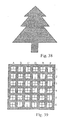
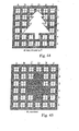
- Figure 38 shows a tree. In this example, it is far from the camera, and takes up only four pixels horizontally and the spaces between them, plus five pixels vertically with spaces.
- Figure 39 represents a small section of the camera sensor, which might be either flat or curved.
- vertical rows are labeled with letters and horizontal rows are labeled with numbers.
- the dark areas represent spaces between the pixels.
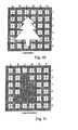
- Figure 40 shows how the tree's image might be first positioned on the pixels. Note that only pixels C2, C3, D3, C4, D4, B5, C5 and D5 are "more covered than not" by the tree image. Those, then, are the pixels that will record its image.
- Figure 41 shows the resulting image that will represent the tree from this single exposure.
- the blackened pixels will be that first image.
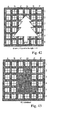
- Figure 42 represents a second exposure. Note that the image for this exposure has been shifted by 1 ⁇ 2 pixel to the right. This shift might be done by moving the sensor physically, or, by reversing the process known in the industry as "image stabilization.” Image stabilization is a method to eliminate blur caused by camera movement during exposures. Reversing that process to move the image focused on the sensor, for the additional exposures, and reversing only between those exposures, is a unique concept and is claimed for this invention.
- Figure 44 represents a third exposure. This time the image is moved up from exposure 2 by 1 ⁇ 2 pixel. The results are that the tree is picked up on pixels D2, C3, D3, C4, D4, E4 and D5.
- Figure 46 continues the example.
- the image is now shifted to the left by 1 ⁇ 2 pixel from the third exposure.
- the result is that imagery is caught by pixels C2, C3, D3, B4, C4, D4 and C5.
- Figure 47 represents that fourth recorded image.
- the camera has four views of the same tree image.
- Pixel response times are also improving regularly, to the point that digital cameras that were formerly only still cameras, have, for the most part, also become motion picture cameras in subsequent model enhancements. This also suggests that rapid multiple exposures can be done; particularly since this is the essence of motion photography.
- the software looks at all four figures and determine that whatever this is, it has a base that's above that stub, and that base is wider than the rest of the image, going three pixels horizontally. This comes from line five in Figures 41 and 43 plus line four in Figures 45 and 47 .
- the software looks at lines three and four in Figure 41 and Figure 43 and conclude that there is a second tier above the broad base in this image, whatever it is, that is two pixels wide and two pixels tall.
- the software averages these different conclusions and make the second tier 1 1 ⁇ 2 pixels tall.
- the software looks at line two in all four images and realize that there is a narrower yet image atop the second tier. This image is consistently one pixel wide and one pixel high, sits atop the second tier but is always centered over the widest bottom tier, and the stub when the stub appears.
- Figure 48 shows the resulting data image recorded by taking four images, each 1 ⁇ 2 pixel apart from the adjoining exposures taken. Note that since the data has four times as much information, the composite image, whether on screen or printed out, will produce 1/4 fractions of pixels. This shows detail that the sensor screen was incapable of capturing with a single exposure.
- Figure 49 shows the original tree image, as it would be digitally recorded in four varying exposures on the sensor, each positioned 1 ⁇ 2 pixel apart.
- Figure 49 shows the tree itself, and the four typical digital images that would be recorded by four individual exposures of that tree. None look anything like a tree.
- Figure 50 shows how the original tree breaks down into the multiple images, and, how the composite, created by the software from those four images, starts to resemble a tree.
- the resemblance is obviously not perfect, but is closer. Considering that this represents about 0.000001% of the image area, this resemblance could help some surveillance situations.
- One embodiment of this new method proposes to create a concave mold to shape the silicon after heating the wafer to a nearly molten state. Gravity then settles the silicon into the mold. In all of these methods, the mold or molds could be chilled to maintain the original thickness uniformly by reducing the temperature quickly. Centrifuging is a second possible method. The third is air pressure relieved by porosity in the mold. A fourth is steam, raised in temperature by pressure and/or a liquid used with a very high boiling point. The fourth is simply pressing a convex mold onto the wafer, forcing it into the concave mold, but again, doing so after raising the temperature of the silicon.
- Heating can occur in several ways.
- Conventional "baking" is one. Selecting a radiation frequency that affects the silicon significantly more than any of the other materials is a second method. To enhance that second method, a lampblack-like material that absorbs most of the radiation might be placed on the side of the silicon that's to become convex, and is removed later. It absorbs the radiation, possibly burns off in the process but heats the thickness of the wafer unevenly, warming the convex side the most, which is where the most stretching occurs.
- a third method might be to put this radiation absorbing material on both surfaces, so the concave side, which absorbs compression tension and the convex side, which is pulled by tensile stresses, are each heated to manage these changes without fracturing.
- a final method is simply machining, polishing or laser etching away the excess material to create the curved sensor.
- the curved surface is machined out of the silicon or other ingot material.
- the ingot would be thicker than ordinary wafers. Machining could be mechanical, by laser, ions or other methods.
- the wafer material is placed over a pattern of concave discs. Flash heating lets the material drop into the concave shape. This may be simply gravity induced, or, in another embodiment, may be centrifuged.
- Another enhancement may be to "paint" the backside with a specific material that absorbs a certain frequency of radiation to heat the backside of the silicon or other material while transmitting less heat to the middle of the sensor. This gives the silicon or other material the most flexibility across the side being stretched to fit the mold while the middle, is less heated, holding the sensor together and not being compressed or stretched, but only bent.
- the frontside is "painted” and irradiated, to allow that portion to compress without fracturing.
- both sides are heated at the same time, just before reforming.
- Radiation frequency and the absorbent "paint" would be selected to minimize or eliminate any effect on the dopants if already inserted.
- a generally constant motion is deliberately imparted to a sensor and/or an optical element while multiple exposures are taken.
- this motion may be intermittent.
- Software then processes the multiple exposures to provide an enhanced image that offers greater definition and edge detail.
- the software takes as many exposures as the user may predetermine.
- the senor is arrayed with pixels having a variable density, with the highest density in the center of the sensors.
- the motion on the outer edges is far greater than at the center.
- the pixels at the outer edges, where they are least densely placed will be the largest individual pixels.
- the center pixels, where concentration is greatest, will have the smallest pixels. In between those extremes, the sizes will gradually change and grow as the distance from the center increases. In this way, for a fraction of a degree in rotation, the same amount of pixel change across the image takes place, and, image definition can be enhanced in this rotating direction.
- a second exposure is taken with a fraction of a pixel's rotation, more edge detail of the image is captured and enhanced.
- a stationary flat or curved sensor may be used to collect data or to produce an image using an image which moves in a circular motion.
- the circular path of the image has a diameter which is generally less than the width of a pixel on the sensor. In one embodiment, the circular path has a diameter which is half the width of a pixel. In this embodiment, pixel density is constant across the sensor. If the image was a picture of a clock, it would move constantly in a small circle, with the number 12 always on top and the number 6 always on the bottom.
- a flat or curved sensor which generally constantly moves in a tight circle may be used to collect data or to produce an image.
- the circular path of the moving sensor has a diameter which is generally less than the width of a pixel on the sensor.
- the circular path has a diameter which is half the width of a pixel.
- the circular paths might have diameters of four and one half pixels, or six and one quarter pixels, or some other suitable diameter.
- the invention may be implemented using any movement that results in capturing added fractional images to provide detail beyond the normal pixel count's ability to detect.
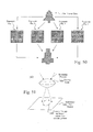
- Figure 51 presents a schematic illustration 342 of an optical element 344 which moves over a flat sensor 346.
- the optical element 344 moves in a tight circular path over the flat sensor to move the incoming light over the surface of the flat sensor along a tight circular path 348.
- the optical element is shown as an objective lens. In other embodiments, any other suitable lens or optical component may be employed.
- the optical element 344 may tilt or nutate back and forth in a generally continuous or intermittent motion that moves the image in a tight circle over the surface of the stationary flat sensor 346.
- Figure 52 is an overhead view 350 of the same optical element 344 which moves over a the same stationary flat sensor 346 as shown in Figure 51 .
- the optical element 344 moves in a tight circular path over the sensor 346 to move the incoming light over the surface of the flat sensor 346.
- Figure 53 furnishes a schematic illustration 352 of an optical element 344 which moves over a stationary curved sensor 354.
- Figure 54 is an overhead view 356 of the same optical element 344 and sensor 354 shown in Figure 53 .
- Figure 55 supplies a schematic illustration 358 of one method for imparting motion to a flat sensor 360 as it moves beneath a stationary optical element 362.
- Figure 56 is an overhead view 372 of the same stationary optical element 362 and sensor 360 as shown in Figure 55 .
- Figure 57 is an illustration 364 that reveals the details of the components which impart the spinning motion to the sensor 360 shown in Figures 55 and 56 .
- the flat sensor 360 is attached to a post or connector 364 which is mounted on a spinning disc 366 which is positioned below the sensor 360.
- the attachment is made at an off-center location 368 on the disc which is not the center of the disc.
- the disc is rotated by an electric motor 370, which is positioned below the disc.
- the axis 372 of the motor is not aligned with the attachment point 368 of the connecting post 364.
- Figure 58 offers a perspective view of the components shown in Figure 57 .
- Figure 59 offers a schematic depiction 374 of a stationary optical element 362 which resides over a curved sensor 376 which moves below the fixed optical element 362.
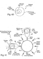
- Figure 60 is an overhead view of the optical element 362 and sensor 376 shown in Figure 59 .
- Figure 61 furnishes an illustration 378 of a method for imparting a circular motion to an optical element 344 like the one shown in Figures 51 and 52 .
- the optical element 344 is surrounded by a band 380, which provides pivoting attachment points 382 for a number of springs 384.
- Two of the springs are attached to cams 386 and 388, and each cam is mounted on an electric motor 390 and 392. When the cams rotate, the springs connected to the bands which surround the optical elements move the optical element.
- the two cams are out of phase by ninety degrees to provide circular motion.
- Figure 62 presents a series 394 of nine simplified views of a flat sensor as it moves through a single orbit in its circular path.
- the circular path is less than one pixel in diameter.
- an axis of rotation C is shown, which lies near the lower left corner of the square sensor.
- a radius segment is shown in each successive view, which connects the axis of rotation to a point on the top side of each square.
- the square sensor has moved forty-five degrees in a clockwise direction about the axis of rotation, C.
- a dotted-line version of the original square is shown in its original position.
- the radius segments are numbered r 1 through r 9 , as they move through each of the eight steps in the circle.
- the senor depicted in Figure 62 may be configured in a rectangular or other suitable planar shape. In another alternative embodiment, the sensor may be curved or hemispherical. The motion may be clockwise, counter-clockwise or any other suitable displacement of position that accomplishes the object of the invention.
- Figure 63 is a schematic representation of a flat sensor arrayed with pixels 396.
- the sensor resides in its original position.
- the sensor continues to rotate through the circular path. As the sensor rotates multiple exposures are taken, as determined by software.
- the outer and inner rows of pixels each move by the same number of pixel spaces.
- This embodiment enhances detail in an image beyond a sensor's pixel count, and may be used in combination with the method described in Section V, above, "Method to Capture More Detail from a Scene than the Sensor is Otherwise Capable of Recording.”
- This embodiment may be utilized in combination with methods and apparatus for sensor connections described in Co-Pending U.S. Patent Application Serial No. 12/655,819, filed on 6 January 2010 , U.S. Patent Publication No. US2010/0260494 ; See, especially, Paragraphs 101 - 113.
- miniature radios may be used to connect the output of the sensor to a micro-processor.
- a sensor is formed from a fabric woven from silicon fibers. While this embodiment employs silicon fibers, the invention may be practiced using any light transmissive fiber material that is suitable for this purpose.
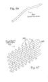
- Figure 66 shows a single strand of silicon fiber 400, which has been manufactured from silicon.
- Figure 67 shows two sets of these fibers 400 which are being woven into a fabric 402. A first set of fibers is positioned so that they are all generally parallel to each other.
- a second set of fibers, which are positioned so that they are orthogonal to the first set of fibers, is then sequentially woven into the first set by threading each fiber over and then below each successive fiber.
- the first set of parallel fibers is called the "warp,” while the set that is woven into the warp by threading under and then over each successive thread is called the “weft.” Since the silicon threads will be fused by heat into a solid fabric, the weave need not be done over and under each thread, but, could be every other thread, every tenth thread, or other number. If ten warp threads were woven over and under ten weft threads, as one possible example, they could be woven together as ten threads. Alternatively, the first warp thread could go over ten weft threads, while the second warp thread might go over nine weft threads but continue going over and under ten weft threads after that. And, in this example, the third warp thread might go over eight weft threads before continuing the pattern of going over and under ten weft threads until the other end of the fabric.
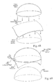
- first mandrel 404 After the fabric 402 is woven, it is placed over a heated first mandrel 404, as shown in Figure 68 .
- the first mandrel 404 has a curved upper surface.
- a second mandrel 505, which has a similar curved shape, is shown above the first mandrel 404.
- the woven fabric takes the shape of the mandrel, is heated, and the silicon fibers fuse together, as shown in Figure 69 .
- a curved sensor 406 is formed, and the excess 408 is trimmed away.
- a group of parallel fibers 410 is be formed into a single unwoven laminate 412, as shown in Figures 70 and 71 .
- the unwoven laminate 412 is pressed between two mandrels, and is then heated.
- the silicon fibers fuse into a curved sensor. Just enough heat is used to make the silicon flexible while on the mandrel, to maintain that state, may be initially warm but could also be quickly chilled to stabilize the silicon into its final hemispherical shape.
- two sets of fibers may be laid at right angles 414, and then heated to form the fused laminate 416, as shown in Figure 72 .
- a curved sensor 418 is formed from a number of generally flat "mini-sensors" which are positioned to form a nearly curved surface. In this embodiment, a slightly different manufacturing process is employed for each successive row of mini-sensors. In alternative embodiments, the sensor may be a conventional planar sensor.
- each mini-sensor is slightly smaller than the adjoining inner row so their corners do not overlap as they tilt inward to create the curve. This creates gaps which were explained in previous portions of this Specification. These gaps also provide shorter average connections to the pixels, so less space is wasted. Since either the image or the sensor itself shift and take double exposures, as explained above, the entire surface captures imagery, creating a virtual 100% "fill factor.” "Fill factor” is the industry phrase that measures the percentage area of a sensor that actually captures photons and converts them to signal data. In this embodiment, each has different pixel densities. The mini-sensor is the center of the entire sensor is the most dense, so digital zoom becomes palatable and crisp without undue expense.
- the next row out is less dense, saving cost, and the same amount of detail which is determined by the total pixel count is captured for normal perspective shots.
- the outside row (this example assumes three rows for simplicity) could is the least detailed, and, being the most numerous, is the cheapest to manufacture.
- center “mini-sensor” is used for the maximum telephoto digital zoom imagery
- the outer row of sixteen "mini-sensors" are 1 MP each. But, since the inner rows and center "mini-sensor" are delivering unnecessary data amounts, they are all compressed to 1 MP each. This delivers a wide angle image of 25 MP, more than the human eye can resolve at an 8" x 10" enlargement.
- This configuration provides cost savings, as well as optimal megapixel counts for all three perspectives: telephoto, normal and wide angle, and for any perspective in between.
- the relatively "sparse" mini-sensors in the outermost ring are formed so that they are much larger than the other mini-sensors that are nearer to the center of the sensor, as shown in Figure 73 .
- the relatively large mini-sensors are more sensitive than the smaller ones toward the center of the sensor.
- the mini-sensors in the center are relatively small, while mini-sensors in each successive larger ring are larger.
- Figure 73 shows a sensor 420 having a center mini-sensor 420, a first ring of mini-sensors 422, a second ring of mini-sensors 424, and an outermost ring of mini-sensors 426.
- this sensor may be generally constantly rotated, as shown in Figure 74 .
- the sensor rotates 0.001 degree, for example, which corresponds to roughly the same fraction of a pixel-to-image shift in all three rings; center, first surrounding ring and the outer ring. Multiple exposures can be used to capture more image detail than the pixel count would seem to suggest, since, the sensor is capturing new fractions of pixel images in subsequent exposures and edges. This method provides detail in a circular direction, but none added in the concentric direction.
- Figure 75 illustrates a section of staggered pixel arrays on a mini-sensor.
Landscapes
- Engineering & Computer Science (AREA)
- Multimedia (AREA)
- Signal Processing (AREA)
- Studio Devices (AREA)
- Air Bags (AREA)
Applications Claiming Priority (3)
| Application Number | Priority Date | Filing Date | Title |
|---|---|---|---|
| US12/930,165 US8654215B2 (en) | 2009-02-23 | 2010-12-28 | Mobile communicator with curved sensor camera |
| US13/065,477 US8957992B2 (en) | 2010-01-06 | 2011-03-21 | Curved sensor camera with moving optical train |
| US13/135,402 US20120159996A1 (en) | 2010-12-28 | 2011-06-30 | Curved sensor formed from silicon fibers |
Publications (3)
| Publication Number | Publication Date |
|---|---|
| EP2472580A2 true EP2472580A2 (fr) | 2012-07-04 |
| EP2472580A3 EP2472580A3 (fr) | 2012-08-01 |
| EP2472580B1 EP2472580B1 (fr) | 2016-08-03 |
Family
ID=56172330
Family Applications (1)
| Application Number | Title | Priority Date | Filing Date |
|---|---|---|---|
| EP11006759.2A Not-in-force EP2472580B1 (fr) | 2010-12-28 | 2011-08-18 | Procédé de fabrication d'un capteur incurvé |
Country Status (1)
| Country | Link |
|---|---|
| EP (1) | EP2472580B1 (fr) |
Citations (1)
| Publication number | Priority date | Publication date | Assignee | Title |
|---|---|---|---|---|
| US20100260494A1 (en) | 2009-02-23 | 2010-10-14 | Gary Edwin Sutton | Curvilinear sensor system |
Family Cites Families (5)
| Publication number | Priority date | Publication date | Assignee | Title |
|---|---|---|---|---|
| JP3610234B2 (ja) * | 1998-07-17 | 2005-01-12 | 株式会社メディア・テクノロジー | アイリス情報取得装置およびアイリス識別装置 |
| US7408572B2 (en) * | 2002-07-06 | 2008-08-05 | Nova Research, Inc. | Method and apparatus for an on-chip variable acuity imager array incorporating roll, pitch and yaw angle rates measurement |
| US20070296842A1 (en) * | 2006-06-09 | 2007-12-27 | Raymond Samuel Connell | Spiral image capture system |
| US7742090B2 (en) * | 2006-12-22 | 2010-06-22 | Palo Alto Research Center Incorporated | Flexible segmented image sensor |
| US8077235B2 (en) * | 2008-01-22 | 2011-12-13 | Palo Alto Research Center Incorporated | Addressing of a three-dimensional, curved sensor or display back plane |
-
2011
- 2011-08-18 EP EP11006759.2A patent/EP2472580B1/fr not_active Not-in-force
Patent Citations (1)
| Publication number | Priority date | Publication date | Assignee | Title |
|---|---|---|---|---|
| US20100260494A1 (en) | 2009-02-23 | 2010-10-14 | Gary Edwin Sutton | Curvilinear sensor system |
Also Published As
| Publication number | Publication date |
|---|---|
| EP2472580B1 (fr) | 2016-08-03 |
| EP2472580A3 (fr) | 2012-08-01 |
Similar Documents
| Publication | Publication Date | Title |
|---|---|---|
| US20120159996A1 (en) | Curved sensor formed from silicon fibers | |
| CA2762725C (fr) | Dispositif de communication portatif avec appareil photo a capteur recourbe | |
| US8957992B2 (en) | Curved sensor camera with moving optical train | |
| US20150189140A1 (en) | Curved sensor array camera | |
| CA2752491C (fr) | Systemes de capteurs et appareils photo numeriques | |
| US8836805B2 (en) | Curved sensor system | |
| US11262558B2 (en) | Methods and apparatus for implementing and/or using a camera device | |
| CN110636277B (zh) | 检测设备、检测方法和摄像设备 | |
| WO2009052333A1 (fr) | Caméra à calcul rapide basée sur deux réseaux de lentilles | |
| JP2016541151A (ja) | カメラデバイスを実施および/または使用するための方法および装置 | |
| KR20150077287A (ko) | 곡면 센서 카메라를 갖는 이동통신장치, 이동형 광학부를 갖는 곡면 센서 카메라, 및 실리콘 섬유로 제작되는 곡면 센서 | |
| KR101488831B1 (ko) | 곡면 센서 카메라를 갖는 이동통신장치, 이동형 광학부를 갖는 곡면 센서 카메라, 및 실리콘 섬유로 제작되는 곡면 센서 | |
| JP5658189B2 (ja) | 曲面状センサーカメラを有する移動通信装置、移動型光学部を有する曲面状センサーカメラ、及びシリコン繊維で製作される曲面状センサー | |
| CA2850811A1 (fr) | Camera a capteur recourbe | |
| US20140118526A1 (en) | Curvilinear sensor system | |
| US20130278818A1 (en) | Curved sensor system | |
| US20150077627A1 (en) | Curved sensor formed from silicon fibers | |
| EP2472580B1 (fr) | Procédé de fabrication d'un capteur incurvé | |
| CA2781986A1 (fr) | Capteur courbe fait de fibres de silicium | |
| US20160013244A1 (en) | Curved sensor system | |
| EP2822265A1 (fr) | Camera avec matrice de capteurs courbée | |
| KR20120053345A (ko) | 복수의 촬상 소자를 갖는 카메라 |
Legal Events
| Date | Code | Title | Description |
|---|---|---|---|
| PUAL | Search report despatched |
Free format text: ORIGINAL CODE: 0009013 |
|
| AK | Designated contracting states |
Kind code of ref document: A2 Designated state(s): AL AT BE BG CH CY CZ DE DK EE ES FI FR GB GR HR HU IE IS IT LI LT LU LV MC MK MT NL NO PL PT RO RS SE SI SK SM TR |
|
| AX | Request for extension of the european patent |
Extension state: BA ME |
|
| PUAI | Public reference made under article 153(3) epc to a published international application that has entered the european phase |
Free format text: ORIGINAL CODE: 0009012 |
|
| AK | Designated contracting states |
Kind code of ref document: A3 Designated state(s): AL AT BE BG CH CY CZ DE DK EE ES FI FR GB GR HR HU IE IS IT LI LT LU LV MC MK MT NL NO PL PT RO RS SE SI SK SM TR |
|
| AX | Request for extension of the european patent |
Extension state: BA ME |
|
| RIC1 | Information provided on ipc code assigned before grant |
Ipc: H01L 27/146 20060101AFI20120628BHEP |
|
| 17P | Request for examination filed |
Effective date: 20130201 |
|
| GRAP | Despatch of communication of intention to grant a patent |
Free format text: ORIGINAL CODE: EPIDOSNIGR1 |
|
| RIC1 | Information provided on ipc code assigned before grant |
Ipc: H01L 27/146 20060101AFI20160128BHEP Ipc: H04N 5/369 20110101ALI20160128BHEP |
|
| INTG | Intention to grant announced |
Effective date: 20160219 |
|
| GRAS | Grant fee paid |
Free format text: ORIGINAL CODE: EPIDOSNIGR3 |
|
| GRAA | (expected) grant |
Free format text: ORIGINAL CODE: 0009210 |
|
| AK | Designated contracting states |
Kind code of ref document: B1 Designated state(s): AL AT BE BG CH CY CZ DE DK EE ES FI FR GB GR HR HU IE IS IT LI LT LU LV MC MK MT NL NO PL PT RO RS SE SI SK SM TR |
|
| REG | Reference to a national code |
Ref country code: GB Ref legal event code: FG4D |
|
| REG | Reference to a national code |
Ref country code: CH Ref legal event code: EP Ref country code: AT Ref legal event code: REF Ref document number: 817849 Country of ref document: AT Kind code of ref document: T Effective date: 20160815 |
|
| REG | Reference to a national code |
Ref country code: IE Ref legal event code: FG4D |
|
| REG | Reference to a national code |
Ref country code: DE Ref legal event code: R096 Ref document number: 602011028718 Country of ref document: DE |
|
| REG | Reference to a national code |
Ref country code: NL Ref legal event code: MP Effective date: 20160803 |
|
| REG | Reference to a national code |
Ref country code: LT Ref legal event code: MG4D |
|
| REG | Reference to a national code |
Ref country code: AT Ref legal event code: MK05 Ref document number: 817849 Country of ref document: AT Kind code of ref document: T Effective date: 20160803 |
|
| PG25 | Lapsed in a contracting state [announced via postgrant information from national office to epo] |
Ref country code: IS Free format text: LAPSE BECAUSE OF FAILURE TO SUBMIT A TRANSLATION OF THE DESCRIPTION OR TO PAY THE FEE WITHIN THE PRESCRIBED TIME-LIMIT Effective date: 20161203 Ref country code: NO Free format text: LAPSE BECAUSE OF FAILURE TO SUBMIT A TRANSLATION OF THE DESCRIPTION OR TO PAY THE FEE WITHIN THE PRESCRIBED TIME-LIMIT Effective date: 20161103 Ref country code: IT Free format text: LAPSE BECAUSE OF FAILURE TO SUBMIT A TRANSLATION OF THE DESCRIPTION OR TO PAY THE FEE WITHIN THE PRESCRIBED TIME-LIMIT Effective date: 20160803 Ref country code: LT Free format text: LAPSE BECAUSE OF FAILURE TO SUBMIT A TRANSLATION OF THE DESCRIPTION OR TO PAY THE FEE WITHIN THE PRESCRIBED TIME-LIMIT Effective date: 20160803 Ref country code: FI Free format text: LAPSE BECAUSE OF FAILURE TO SUBMIT A TRANSLATION OF THE DESCRIPTION OR TO PAY THE FEE WITHIN THE PRESCRIBED TIME-LIMIT Effective date: 20160803 Ref country code: NL Free format text: LAPSE BECAUSE OF FAILURE TO SUBMIT A TRANSLATION OF THE DESCRIPTION OR TO PAY THE FEE WITHIN THE PRESCRIBED TIME-LIMIT Effective date: 20160803 Ref country code: RS Free format text: LAPSE BECAUSE OF FAILURE TO SUBMIT A TRANSLATION OF THE DESCRIPTION OR TO PAY THE FEE WITHIN THE PRESCRIBED TIME-LIMIT Effective date: 20160803 Ref country code: HR Free format text: LAPSE BECAUSE OF FAILURE TO SUBMIT A TRANSLATION OF THE DESCRIPTION OR TO PAY THE FEE WITHIN THE PRESCRIBED TIME-LIMIT Effective date: 20160803 |
|
| PG25 | Lapsed in a contracting state [announced via postgrant information from national office to epo] |
Ref country code: AT Free format text: LAPSE BECAUSE OF FAILURE TO SUBMIT A TRANSLATION OF THE DESCRIPTION OR TO PAY THE FEE WITHIN THE PRESCRIBED TIME-LIMIT Effective date: 20160803 Ref country code: PL Free format text: LAPSE BECAUSE OF FAILURE TO SUBMIT A TRANSLATION OF THE DESCRIPTION OR TO PAY THE FEE WITHIN THE PRESCRIBED TIME-LIMIT Effective date: 20160803 Ref country code: SE Free format text: LAPSE BECAUSE OF FAILURE TO SUBMIT A TRANSLATION OF THE DESCRIPTION OR TO PAY THE FEE WITHIN THE PRESCRIBED TIME-LIMIT Effective date: 20160803 Ref country code: LV Free format text: LAPSE BECAUSE OF FAILURE TO SUBMIT A TRANSLATION OF THE DESCRIPTION OR TO PAY THE FEE WITHIN THE PRESCRIBED TIME-LIMIT Effective date: 20160803 Ref country code: ES Free format text: LAPSE BECAUSE OF FAILURE TO SUBMIT A TRANSLATION OF THE DESCRIPTION OR TO PAY THE FEE WITHIN THE PRESCRIBED TIME-LIMIT Effective date: 20160803 Ref country code: GR Free format text: LAPSE BECAUSE OF FAILURE TO SUBMIT A TRANSLATION OF THE DESCRIPTION OR TO PAY THE FEE WITHIN THE PRESCRIBED TIME-LIMIT Effective date: 20161104 Ref country code: PT Free format text: LAPSE BECAUSE OF FAILURE TO SUBMIT A TRANSLATION OF THE DESCRIPTION OR TO PAY THE FEE WITHIN THE PRESCRIBED TIME-LIMIT Effective date: 20161205 Ref country code: BE Free format text: LAPSE BECAUSE OF NON-PAYMENT OF DUE FEES Effective date: 20160831 |
|
| REG | Reference to a national code |
Ref country code: DE Ref legal event code: R119 Ref document number: 602011028718 Country of ref document: DE |
|
| REG | Reference to a national code |
Ref country code: CH Ref legal event code: PL |
|
| PG25 | Lapsed in a contracting state [announced via postgrant information from national office to epo] |
Ref country code: CH Free format text: LAPSE BECAUSE OF NON-PAYMENT OF DUE FEES Effective date: 20160831 Ref country code: RO Free format text: LAPSE BECAUSE OF FAILURE TO SUBMIT A TRANSLATION OF THE DESCRIPTION OR TO PAY THE FEE WITHIN THE PRESCRIBED TIME-LIMIT Effective date: 20160803 Ref country code: EE Free format text: LAPSE BECAUSE OF FAILURE TO SUBMIT A TRANSLATION OF THE DESCRIPTION OR TO PAY THE FEE WITHIN THE PRESCRIBED TIME-LIMIT Effective date: 20160803 Ref country code: LI Free format text: LAPSE BECAUSE OF NON-PAYMENT OF DUE FEES Effective date: 20160831 |
|
| PG25 | Lapsed in a contracting state [announced via postgrant information from national office to epo] |
Ref country code: CZ Free format text: LAPSE BECAUSE OF FAILURE TO SUBMIT A TRANSLATION OF THE DESCRIPTION OR TO PAY THE FEE WITHIN THE PRESCRIBED TIME-LIMIT Effective date: 20160803 Ref country code: DK Free format text: LAPSE BECAUSE OF FAILURE TO SUBMIT A TRANSLATION OF THE DESCRIPTION OR TO PAY THE FEE WITHIN THE PRESCRIBED TIME-LIMIT Effective date: 20160803 Ref country code: SM Free format text: LAPSE BECAUSE OF FAILURE TO SUBMIT A TRANSLATION OF THE DESCRIPTION OR TO PAY THE FEE WITHIN THE PRESCRIBED TIME-LIMIT Effective date: 20160803 Ref country code: SK Free format text: LAPSE BECAUSE OF FAILURE TO SUBMIT A TRANSLATION OF THE DESCRIPTION OR TO PAY THE FEE WITHIN THE PRESCRIBED TIME-LIMIT Effective date: 20160803 Ref country code: BG Free format text: LAPSE BECAUSE OF FAILURE TO SUBMIT A TRANSLATION OF THE DESCRIPTION OR TO PAY THE FEE WITHIN THE PRESCRIBED TIME-LIMIT Effective date: 20161103 Ref country code: BE Free format text: LAPSE BECAUSE OF FAILURE TO SUBMIT A TRANSLATION OF THE DESCRIPTION OR TO PAY THE FEE WITHIN THE PRESCRIBED TIME-LIMIT Effective date: 20160803 |
|
| REG | Reference to a national code |
Ref country code: IE Ref legal event code: MM4A |
|
| PLBE | No opposition filed within time limit |
Free format text: ORIGINAL CODE: 0009261 |
|
| STAA | Information on the status of an ep patent application or granted ep patent |
Free format text: STATUS: NO OPPOSITION FILED WITHIN TIME LIMIT |
|
| PG25 | Lapsed in a contracting state [announced via postgrant information from national office to epo] |
Ref country code: MC Free format text: LAPSE BECAUSE OF FAILURE TO SUBMIT A TRANSLATION OF THE DESCRIPTION OR TO PAY THE FEE WITHIN THE PRESCRIBED TIME-LIMIT Effective date: 20160803 |
|
| REG | Reference to a national code |
Ref country code: FR Ref legal event code: ST Effective date: 20170602 |
|
| 26N | No opposition filed |
Effective date: 20170504 |
|
| GBPC | Gb: european patent ceased through non-payment of renewal fee |
Effective date: 20161103 |
|
| PG25 | Lapsed in a contracting state [announced via postgrant information from national office to epo] |
Ref country code: DE Free format text: LAPSE BECAUSE OF NON-PAYMENT OF DUE FEES Effective date: 20170301 Ref country code: FR Free format text: LAPSE BECAUSE OF NON-PAYMENT OF DUE FEES Effective date: 20161003 Ref country code: IE Free format text: LAPSE BECAUSE OF NON-PAYMENT OF DUE FEES Effective date: 20160818 |
|
| PG25 | Lapsed in a contracting state [announced via postgrant information from national office to epo] |
Ref country code: LU Free format text: LAPSE BECAUSE OF NON-PAYMENT OF DUE FEES Effective date: 20160818 Ref country code: SI Free format text: LAPSE BECAUSE OF FAILURE TO SUBMIT A TRANSLATION OF THE DESCRIPTION OR TO PAY THE FEE WITHIN THE PRESCRIBED TIME-LIMIT Effective date: 20160803 |
|
| PG25 | Lapsed in a contracting state [announced via postgrant information from national office to epo] |
Ref country code: GB Free format text: LAPSE BECAUSE OF NON-PAYMENT OF DUE FEES Effective date: 20161103 |
|
| PG25 | Lapsed in a contracting state [announced via postgrant information from national office to epo] |
Ref country code: HU Free format text: LAPSE BECAUSE OF FAILURE TO SUBMIT A TRANSLATION OF THE DESCRIPTION OR TO PAY THE FEE WITHIN THE PRESCRIBED TIME-LIMIT; INVALID AB INITIO Effective date: 20110818 Ref country code: CY Free format text: LAPSE BECAUSE OF FAILURE TO SUBMIT A TRANSLATION OF THE DESCRIPTION OR TO PAY THE FEE WITHIN THE PRESCRIBED TIME-LIMIT Effective date: 20160803 |
|
| PG25 | Lapsed in a contracting state [announced via postgrant information from national office to epo] |
Ref country code: TR Free format text: LAPSE BECAUSE OF FAILURE TO SUBMIT A TRANSLATION OF THE DESCRIPTION OR TO PAY THE FEE WITHIN THE PRESCRIBED TIME-LIMIT Effective date: 20160803 Ref country code: MK Free format text: LAPSE BECAUSE OF FAILURE TO SUBMIT A TRANSLATION OF THE DESCRIPTION OR TO PAY THE FEE WITHIN THE PRESCRIBED TIME-LIMIT Effective date: 20160803 Ref country code: MT Free format text: LAPSE BECAUSE OF NON-PAYMENT OF DUE FEES Effective date: 20160831 |
|
| PG25 | Lapsed in a contracting state [announced via postgrant information from national office to epo] |
Ref country code: AL Free format text: LAPSE BECAUSE OF FAILURE TO SUBMIT A TRANSLATION OF THE DESCRIPTION OR TO PAY THE FEE WITHIN THE PRESCRIBED TIME-LIMIT Effective date: 20160803 |