EP2472589A1 - Cellule solaire et son procédé de fabrication - Google Patents
Cellule solaire et son procédé de fabrication Download PDFInfo
- Publication number
- EP2472589A1 EP2472589A1 EP11007238A EP11007238A EP2472589A1 EP 2472589 A1 EP2472589 A1 EP 2472589A1 EP 11007238 A EP11007238 A EP 11007238A EP 11007238 A EP11007238 A EP 11007238A EP 2472589 A1 EP2472589 A1 EP 2472589A1
- Authority
- EP
- European Patent Office
- Prior art keywords
- substrate
- via hole
- reflection layer
- electrode
- disposed
- Prior art date
- Legal status (The legal status is an assumption and is not a legal conclusion. Google has not performed a legal analysis and makes no representation as to the accuracy of the status listed.)
- Granted
Links
- 238000000034 method Methods 0.000 title claims description 28
- 238000004519 manufacturing process Methods 0.000 title claims description 8
- 239000000758 substrate Substances 0.000 claims abstract description 180
- 238000010438 heat treatment Methods 0.000 claims description 13
- 230000000149 penetrating effect Effects 0.000 claims description 10
- 229910052751 metal Inorganic materials 0.000 claims description 7
- 239000002184 metal Substances 0.000 claims description 7
- 239000012535 impurity Substances 0.000 description 14
- PXHVJJICTQNCMI-UHFFFAOYSA-N Nickel Chemical compound [Ni] PXHVJJICTQNCMI-UHFFFAOYSA-N 0.000 description 12
- 230000005684 electric field Effects 0.000 description 12
- 239000004020 conductor Substances 0.000 description 11
- 230000008569 process Effects 0.000 description 11
- BQCADISMDOOEFD-UHFFFAOYSA-N Silver Chemical compound [Ag] BQCADISMDOOEFD-UHFFFAOYSA-N 0.000 description 9
- 229910052709 silver Inorganic materials 0.000 description 9
- 239000004332 silver Substances 0.000 description 9
- 229910052782 aluminium Inorganic materials 0.000 description 8
- XAGFODPZIPBFFR-UHFFFAOYSA-N aluminium Chemical compound [Al] XAGFODPZIPBFFR-UHFFFAOYSA-N 0.000 description 8
- 239000010949 copper Substances 0.000 description 8
- 239000010931 gold Substances 0.000 description 8
- 239000004065 semiconductor Substances 0.000 description 8
- 239000010936 titanium Substances 0.000 description 8
- VYPSYNLAJGMNEJ-UHFFFAOYSA-N Silicium dioxide Chemical compound O=[Si]=O VYPSYNLAJGMNEJ-UHFFFAOYSA-N 0.000 description 6
- XUIMIQQOPSSXEZ-UHFFFAOYSA-N Silicon Chemical compound [Si] XUIMIQQOPSSXEZ-UHFFFAOYSA-N 0.000 description 6
- HEMHJVSKTPXQMS-UHFFFAOYSA-M Sodium hydroxide Chemical compound [OH-].[Na+] HEMHJVSKTPXQMS-UHFFFAOYSA-M 0.000 description 6
- TWNQGVIAIRXVLR-UHFFFAOYSA-N oxo(oxoalumanyloxy)alumane Chemical compound O=[Al]O[Al]=O TWNQGVIAIRXVLR-UHFFFAOYSA-N 0.000 description 6
- 229910052710 silicon Inorganic materials 0.000 description 6
- 239000010703 silicon Substances 0.000 description 6
- 229910052814 silicon oxide Inorganic materials 0.000 description 6
- 239000011521 glass Substances 0.000 description 5
- 229910052738 indium Inorganic materials 0.000 description 5
- APFVFJFRJDLVQX-UHFFFAOYSA-N indium atom Chemical compound [In] APFVFJFRJDLVQX-UHFFFAOYSA-N 0.000 description 5
- 239000000463 material Substances 0.000 description 5
- RYGMFSIKBFXOCR-UHFFFAOYSA-N Copper Chemical compound [Cu] RYGMFSIKBFXOCR-UHFFFAOYSA-N 0.000 description 4
- 229910052581 Si3N4 Inorganic materials 0.000 description 4
- ATJFFYVFTNAWJD-UHFFFAOYSA-N Tin Chemical compound [Sn] ATJFFYVFTNAWJD-UHFFFAOYSA-N 0.000 description 4
- GWEVSGVZZGPLCZ-UHFFFAOYSA-N Titan oxide Chemical compound O=[Ti]=O GWEVSGVZZGPLCZ-UHFFFAOYSA-N 0.000 description 4
- RTAQQCXQSZGOHL-UHFFFAOYSA-N Titanium Chemical compound [Ti] RTAQQCXQSZGOHL-UHFFFAOYSA-N 0.000 description 4
- 229910052802 copper Inorganic materials 0.000 description 4
- PCHJSUWPFVWCPO-UHFFFAOYSA-N gold Chemical compound [Au] PCHJSUWPFVWCPO-UHFFFAOYSA-N 0.000 description 4
- 229910052737 gold Inorganic materials 0.000 description 4
- 229910021478 group 5 element Inorganic materials 0.000 description 4
- 229910052759 nickel Inorganic materials 0.000 description 4
- 230000006798 recombination Effects 0.000 description 4
- 238000005215 recombination Methods 0.000 description 4
- HQVNEWCFYHHQES-UHFFFAOYSA-N silicon nitride Chemical compound N12[Si]34N5[Si]62N3[Si]51N64 HQVNEWCFYHHQES-UHFFFAOYSA-N 0.000 description 4
- JBQYATWDVHIOAR-UHFFFAOYSA-N tellanylidenegermanium Chemical compound [Te]=[Ge] JBQYATWDVHIOAR-UHFFFAOYSA-N 0.000 description 4
- 229910052719 titanium Inorganic materials 0.000 description 4
- 230000007547 defect Effects 0.000 description 3
- 238000001035 drying Methods 0.000 description 3
- 239000007789 gas Substances 0.000 description 3
- 230000001788 irregular Effects 0.000 description 3
- 229910021421 monocrystalline silicon Inorganic materials 0.000 description 3
- 238000000623 plasma-assisted chemical vapour deposition Methods 0.000 description 3
- 229910021420 polycrystalline silicon Inorganic materials 0.000 description 3
- 238000007650 screen-printing Methods 0.000 description 3
- ZOXJGFHDIHLPTG-UHFFFAOYSA-N Boron Chemical compound [B] ZOXJGFHDIHLPTG-UHFFFAOYSA-N 0.000 description 2
- OAICVXFJPJFONN-UHFFFAOYSA-N Phosphorus Chemical compound [P] OAICVXFJPJFONN-UHFFFAOYSA-N 0.000 description 2
- KWYUFKZDYYNOTN-UHFFFAOYSA-M Potassium hydroxide Chemical compound [OH-].[K+] KWYUFKZDYYNOTN-UHFFFAOYSA-M 0.000 description 2
- 229910004205 SiNX Inorganic materials 0.000 description 2
- 229910020286 SiOxNy Inorganic materials 0.000 description 2
- 229910052787 antimony Inorganic materials 0.000 description 2
- WATWJIUSRGPENY-UHFFFAOYSA-N antimony atom Chemical compound [Sb] WATWJIUSRGPENY-UHFFFAOYSA-N 0.000 description 2
- 229910052785 arsenic Inorganic materials 0.000 description 2
- RQNWIZPPADIBDY-UHFFFAOYSA-N arsenic atom Chemical compound [As] RQNWIZPPADIBDY-UHFFFAOYSA-N 0.000 description 2
- 229910052796 boron Inorganic materials 0.000 description 2
- 238000005229 chemical vapour deposition Methods 0.000 description 2
- 238000005520 cutting process Methods 0.000 description 2
- 229910052739 hydrogen Inorganic materials 0.000 description 2
- 239000001257 hydrogen Substances 0.000 description 2
- 238000002161 passivation Methods 0.000 description 2
- 230000035515 penetration Effects 0.000 description 2
- XHXFXVLFKHQFAL-UHFFFAOYSA-N phosphoryl trichloride Chemical compound ClP(Cl)(Cl)=O XHXFXVLFKHQFAL-UHFFFAOYSA-N 0.000 description 2
- 239000005368 silicate glass Substances 0.000 description 2
- 238000005507 spraying Methods 0.000 description 2
- WGTYBPLFGIVFAS-UHFFFAOYSA-M tetramethylammonium hydroxide Chemical compound [OH-].C[N+](C)(C)C WGTYBPLFGIVFAS-UHFFFAOYSA-M 0.000 description 2
- OGIDPMRJRNCKJF-UHFFFAOYSA-N titanium oxide Inorganic materials [Ti]=O OGIDPMRJRNCKJF-UHFFFAOYSA-N 0.000 description 2
- GYHNNYVSQQEPJS-UHFFFAOYSA-N Gallium Chemical compound [Ga] GYHNNYVSQQEPJS-UHFFFAOYSA-N 0.000 description 1
- UFHFLCQGNIYNRP-UHFFFAOYSA-N Hydrogen Chemical compound [H][H] UFHFLCQGNIYNRP-UHFFFAOYSA-N 0.000 description 1
- GRYLNZFGIOXLOG-UHFFFAOYSA-N Nitric acid Chemical compound O[N+]([O-])=O GRYLNZFGIOXLOG-UHFFFAOYSA-N 0.000 description 1
- 229910019213 POCl3 Inorganic materials 0.000 description 1
- NBIIXXVUZAFLBC-UHFFFAOYSA-N Phosphoric acid Chemical compound OP(O)(O)=O NBIIXXVUZAFLBC-UHFFFAOYSA-N 0.000 description 1
- 239000002253 acid Substances 0.000 description 1
- 230000003466 anti-cipated effect Effects 0.000 description 1
- 230000015572 biosynthetic process Effects 0.000 description 1
- 230000008859 change Effects 0.000 description 1
- 239000003245 coal Substances 0.000 description 1
- 230000003247 decreasing effect Effects 0.000 description 1
- 230000008034 disappearance Effects 0.000 description 1
- 238000005553 drilling Methods 0.000 description 1
- 238000010292 electrical insulation Methods 0.000 description 1
- 238000005530 etching Methods 0.000 description 1
- 229910052733 gallium Inorganic materials 0.000 description 1
- BHEPBYXIRTUNPN-UHFFFAOYSA-N hydridophosphorus(.) (triplet) Chemical compound [PH] BHEPBYXIRTUNPN-UHFFFAOYSA-N 0.000 description 1
- 150000002431 hydrogen Chemical class 0.000 description 1
- 230000006872 improvement Effects 0.000 description 1
- 230000001678 irradiating effect Effects 0.000 description 1
- 238000002955 isolation Methods 0.000 description 1
- 239000000203 mixture Substances 0.000 description 1
- 229910017604 nitric acid Inorganic materials 0.000 description 1
- 238000001579 optical reflectometry Methods 0.000 description 1
- 239000003208 petroleum Substances 0.000 description 1
- 229910052698 phosphorus Inorganic materials 0.000 description 1
- 239000011574 phosphorus Substances 0.000 description 1
- 238000005036 potential barrier Methods 0.000 description 1
- 230000009467 reduction Effects 0.000 description 1
- 238000002310 reflectometry Methods 0.000 description 1
- 238000003980 solgel method Methods 0.000 description 1
- 238000004528 spin coating Methods 0.000 description 1
- 239000000126 substance Substances 0.000 description 1
Images




Classifications
-
- H—ELECTRICITY
- H10—SEMICONDUCTOR DEVICES; ELECTRIC SOLID-STATE DEVICES NOT OTHERWISE PROVIDED FOR
- H10F—INORGANIC SEMICONDUCTOR DEVICES SENSITIVE TO INFRARED RADIATION, LIGHT, ELECTROMAGNETIC RADIATION OF SHORTER WAVELENGTH OR CORPUSCULAR RADIATION
- H10F77/00—Constructional details of devices covered by this subclass
- H10F77/30—Coatings
- H10F77/306—Coatings for devices having potential barriers
- H10F77/311—Coatings for devices having potential barriers for photovoltaic cells
- H10F77/315—Coatings for devices having potential barriers for photovoltaic cells the coatings being antireflective or having enhancing optical properties
-
- H—ELECTRICITY
- H10—SEMICONDUCTOR DEVICES; ELECTRIC SOLID-STATE DEVICES NOT OTHERWISE PROVIDED FOR
- H10F—INORGANIC SEMICONDUCTOR DEVICES SENSITIVE TO INFRARED RADIATION, LIGHT, ELECTROMAGNETIC RADIATION OF SHORTER WAVELENGTH OR CORPUSCULAR RADIATION
- H10F10/00—Individual photovoltaic cells, e.g. solar cells
- H10F10/10—Individual photovoltaic cells, e.g. solar cells having potential barriers
- H10F10/14—Photovoltaic cells having only PN homojunction potential barriers
-
- H—ELECTRICITY
- H10—SEMICONDUCTOR DEVICES; ELECTRIC SOLID-STATE DEVICES NOT OTHERWISE PROVIDED FOR
- H10F—INORGANIC SEMICONDUCTOR DEVICES SENSITIVE TO INFRARED RADIATION, LIGHT, ELECTROMAGNETIC RADIATION OF SHORTER WAVELENGTH OR CORPUSCULAR RADIATION
- H10F77/00—Constructional details of devices covered by this subclass
- H10F77/20—Electrodes
- H10F77/206—Electrodes for devices having potential barriers
- H10F77/211—Electrodes for devices having potential barriers for photovoltaic cells
-
- H—ELECTRICITY
- H10—SEMICONDUCTOR DEVICES; ELECTRIC SOLID-STATE DEVICES NOT OTHERWISE PROVIDED FOR
- H10F—INORGANIC SEMICONDUCTOR DEVICES SENSITIVE TO INFRARED RADIATION, LIGHT, ELECTROMAGNETIC RADIATION OF SHORTER WAVELENGTH OR CORPUSCULAR RADIATION
- H10F77/00—Constructional details of devices covered by this subclass
- H10F77/20—Electrodes
- H10F77/206—Electrodes for devices having potential barriers
- H10F77/211—Electrodes for devices having potential barriers for photovoltaic cells
- H10F77/219—Arrangements for electrodes of back-contact photovoltaic cells
- H10F77/227—Arrangements for electrodes of back-contact photovoltaic cells for emitter wrap-through [EWT] photovoltaic cells, e.g. interdigitated emitter-base back-contacts
-
- H—ELECTRICITY
- H10—SEMICONDUCTOR DEVICES; ELECTRIC SOLID-STATE DEVICES NOT OTHERWISE PROVIDED FOR
- H10F—INORGANIC SEMICONDUCTOR DEVICES SENSITIVE TO INFRARED RADIATION, LIGHT, ELECTROMAGNETIC RADIATION OF SHORTER WAVELENGTH OR CORPUSCULAR RADIATION
- H10F77/00—Constructional details of devices covered by this subclass
- H10F77/93—Interconnections
- H10F77/933—Interconnections for devices having potential barriers
- H10F77/935—Interconnections for devices having potential barriers for photovoltaic devices or modules
- H10F77/937—Busbar structures for modules
-
- Y—GENERAL TAGGING OF NEW TECHNOLOGICAL DEVELOPMENTS; GENERAL TAGGING OF CROSS-SECTIONAL TECHNOLOGIES SPANNING OVER SEVERAL SECTIONS OF THE IPC; TECHNICAL SUBJECTS COVERED BY FORMER USPC CROSS-REFERENCE ART COLLECTIONS [XRACs] AND DIGESTS
- Y02—TECHNOLOGIES OR APPLICATIONS FOR MITIGATION OR ADAPTATION AGAINST CLIMATE CHANGE
- Y02E—REDUCTION OF GREENHOUSE GAS [GHG] EMISSIONS, RELATED TO ENERGY GENERATION, TRANSMISSION OR DISTRIBUTION
- Y02E10/00—Energy generation through renewable energy sources
- Y02E10/50—Photovoltaic [PV] energy
- Y02E10/547—Monocrystalline silicon PV cells
Definitions
- Embodiments relates to a solar cell and a method for manufacturing the same.
- a back contact type solar cell which improves efficiency of the solar cell by increasing a light receiving area in such a way to form both of an electrode for outputting electrons to an external device and an electrode for outputting holes to the external device on the back surface of a substrate, namely on the surface located in the opposite of the surface on which light rays are incident.
- Embodiments of the invention provide a solar cell and a method for manufacturing the same capable of improving efficiency of the solar cell and reducing a manufacturing time of the solar cell.
- a solar cell including a substrate of a first conductivity type, the substrate having a via hole, an emitter disposed at the substrate and having a second conductivity type that is opposite the first conductivity type, an anti-reflection layer disposed on a first surface of the substrate and inside the via hole, a first electrode disposed on the first surface of the substrate and in the via hole, a first electrode bus bar disposed on a second surface of the substrate that is opposite the first surface and in the via hole, and a second electrode disposed on the second surface of the substrate and connected to the substrate.
- a position of an end part of the anti-reflection layer inside the via hole may be lower than a position of an end part of the first electrode extending from the first surface to the inside of the via hole.
- the anti-reflection layer may include at least one layer.
- the anti-reflection layer may include at least one of silicon nitride, silicon oxide, aluminum oxide, titanium oxide, and silicon oxynitride.
- the anti-reflection layer may include a plurality of layers, and wherein a number of layers of the anti-reflection layer existing inside the via hole at a position that is closer to the first surface of the substrate is greater than a number of layers of the anti-reflection layer existing inside the via hole at a position that is farther to the first surface of the substrate.
- the solar cell according to the aspect may further include a second bus bar disposed on the second surface of the substrate and connected to the second electrode.
- the first surface may be a light incident surface of the solar cell.
- the first electrode bus bar may contact a portion of the anti-reflection layer that is inside the via hole.
- the anti-reflection layer may include a first portion that is disposed on the first surface of the substrate, and a second portion that is inside the via hole, and wherein the first portion may be discontinuous from the second portion.
- a portion of the first electrode bus bar that is disposed in the via hole may cover the second portion of the anti-reflection layer.
- the second portion of the anti-reflection layer may contact a portion of the first electrode that is in the via hole, a portion of the first electrode bus bar that is in the via hole, and a portion of the emitter that is in the via hole.
- a method for manufacturing a solar cell including forming a via hole in a substrate of a first conductivity type, forming an emitter of a second conductivity type that is opposite the first conductivity type at the substrate, forming an anti-reflection layer on a first surface of the substrate and inside the via hole, forming a bus bar pattern on a second surface of the substrate that is opposite the first surface and inside the via hole by using a first paste, forming a first electrode pattern connected to the bus bar pattern on the first surface and inside the via hole by using a second paste, forming a second electrode pattern on the second surface by using a third paste, and by applying a heat treatment to the substrate with the bus bar pattern, the first electrode pattern and the second electrode pattern, respectively forming a first electrode connected to the emitter by penetrating the anti-reflection layer, a bus bar connected to the first electrode through the via hole, and a second electrode connected to the substrate.
- the first, second and third pastes may be different from each other.
- the first paste may contain a same metal component as the second paste, but a different metal component from the third paste.
- the first and second pastes may contain silver (Ag) and the third paste contains aluminum (Al).
- a position of an end part of the anti-reflection layer may be lower than a position of an end part of the first electrode pattern extending from the first surface of the substrate to the inside of the via hole.
- the forming of the anti-reflection layer may form the anti-reflection layer with at least one layer.
- the forming of the anti-reflection layer may form the anti-reflection layer including at least one of silicon nitride, silicon oxide, aluminum oxide, titanium oxide, and silicon oxynitride.
- the forming of the anti-reflection layer may form the anti-reflection layer with a plurality of layers, and wherein a number of layers of the anti-reflection layer existing inside the via hole at a position that is closer to the first surface of the substrate may be greater than a number of layers of the anti-reflection layer existing inside the via hole at a position that is farther to the first surface of the substrate.
- the anti-reflection layer may be formed to include a first portion that is disposed on the first surface of the substrate, and a second portion that is inside the via hole, and wherein the first portion may be discontinuous from the second portion.
- FIG. 1 is a partial perspective view of a solar cell according to an example embodiment of the invention.
- FIG. 2 is a cross sectional view obtained by cutting the solar cell of FIG. 1 along II-II line;
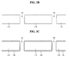
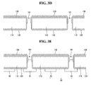
- FIGS. 3A to 3H are cross-sectional views that sequentially illustrate each of stages in a method for manufacturing a solar cell according to an example embodiment of the invention.
- FIG. 4 is a cross sectional view obtained by cutting the solar cell of FIG. 1 along II-II line when the anti-reflection portion of the solar cell is made of a triple layer.
- FIGS. 1 and 2 Now, a solar cell according to an example embodiment of the invention will be described with reference to FIGS. 1 and 2 .
- a solar cell 11 comprises a substrate 110 having a plurality of via holes 181, an emitter 120 disposed in (at) the substrate 110, an anti-reflection layer 130 disposed on the emitter 120 of a surface (hereinafter, referred to as a 'front surface') of the substrate 110, where the front surface is a light incident surface, a plurality of front electrodes 141 disposed on the emitter 120 of the front surface of the substrate 110 in which the anti-reflection layer 130 is not disposed, a back electrode 151 disposed on another surface (hereinafter, referred to as a 'back surface') of the substrate 110, where the back surface is disposed opposite to the front surface of the substrate 110, on which light rays are incident, a plurality of bus bars (hereinafter, referred to as 'a plurality of front electrode bus bars') 161 for the plurality of front electrodes 141, disposed in the via holes 181 and on the
- the substrate 110 is a substrate of a first conductivity type, e.g., a semiconductor substrate made of a semiconductor such as p-type silicon.
- semiconductor is a crystalline semiconductor such as polycrystalline or monocrystalline silicon.
- the substrate 110 When the substrate 110 is of a p-type, the substrate 110 includes impurities of a group III element such as boron (B), gallium (Ga), and indium (In). Alternatively, the substrate 110 may be of an n-type, and/or be formed of materials other than silicon. When the substrate 110 is of the n-type, the substrate 110 may include impurities of a group V element such as phosphor (P), arsenic (As), and antimony (Sb).
- a group III element such as boron (B), gallium (Ga), and indium (In).
- the substrate 110 may be of an n-type, and/or be formed of materials other than silicon.
- the substrate 110 When the substrate 110 is of the n-type, the substrate 110 may include impurities of a group V element such as phosphor (P), arsenic (As), and antimony (Sb).
- the front surface of the substrate 110 is textured, having an irregular textured surface.
- FIG. 1 depicts only the periphery of the substrate 110 as being formed with a textured surface, and depicts only the periphery of the anti-reflection layer 130 disposed on a top thereof as being formed with an irregular surface.
- the entire surface of the substrate 110 has a textured surface, and due to this reason, the anti-reflection layer 130 disposed on the top of the front surface also has an irregular surface.
- not only the front surface, but also the back surface of the substrate 110 can have a textured surface.
- the surface area of the substrate 110 increases, to thereby increasing an area of a light incident surface and decreasing an amount of light reflected by the substrate 110, and therefore, the amount of light incident on the substrate 110 is increased.
- the emitter 120 is an impurity area having a second conductivity type which is opposite to the conductivity type of the substrate 110, and is, for example, an n-type. Due to this, the emitter 120 forms a p-n junction with the first conductivity type part of the substrate 110.
- the emitter 120 forms the p-n junction with the substrate 110, in a different embodiment of the invention, when the substrate 110 is of the n-type, and the emitter 120 is of the p-type, the electrons move to the substrate 110 while the holes move to the emitter 120.
- the emitter 120 when the emitter 120 is of the n-type, the emitter 120 can be doped with impurities of a group V element, whereas in the different embodiment of the invention, when the emitter 120 is of the p-type, the emitter 120 can be doped with impurities of a group III element.
- the anti-reflection layer 130 disposed on the emitter 120 of the front surface of the substrate 110 is made of one from among silicon nitride (SiNx), silicon oxide (SiOx), aluminum oxide (Al 2 O 3 ), titanium oxide (TiO 2 ), and silicon oxynitride (SiOxNy).
- the anti-reflection layer 130 reduces reflectivity of light incident on the solar cell 11 and increases selectivity of particular wavelengths (or bands of wavelengths) of the incident light, thereby increasing the efficiency of the solar cell 11.
- the anti-reflection layer 130 performs a passivation function through hydrogen (H) that was injected when the anti-reflection layer 130 was being formed.
- H hydrogen
- the anti-reflection layer 130 improves the passivation function of the anti-reflection layer 130 in reducing disappearance of charges which have moved toward the surface of the substrate 110 due to the defects. Therefore, since the amount of charges lost near and on the surface of the substrate 110 due to the defect is reduced, efficiency of a solar cell 11 is improved.
- FIG. 1 shows the anti-reflection layer 130 having a single layered structure, but in other embodiments, the anti-reflection layer 130 may have a multi-layered structure such as a double or a triple layered structure.
- each layer of the anti-reflection layer 130 may be made of one from among silicon nitride (SiNx), silicon oxide (SiOx), aluminum oxide (Al 2 O 3 ), titanium oxide (TiO 2 ), and silicon oxynitride (SiOxNy).
- the anti-reflection layer 130 is disposed at each via hole 181.
- the anti-reflection layer 130 has a triple layered structure such as first, second and third anti-reflection layers 131, 132 and 133
- the number of layers formed varies according to an internal position of each via hole 181. Therefore, the number of layers laminated inside each via hole 181 is increased as a position of the via hole 181 that are closer to the area adjacent to where a process gas in the form of vaporized state is sprayed to form each layer of the anti-reflection layer 130, for example, the front surface of the substrate 110 of FIG. 4 .
- FIG. 4 shows that show that are closer to the area adjacent to where a process gas in the form of vaporized state is sprayed to form each layer of the anti-reflection layer 130, for example, the front surface of the substrate 110 of FIG. 4 .
- a thickness of each layer can be varied according to a position of the layer, namely, according to distance from where the process gas is sprayed. Therefore, as the layer is formed closer to the front surface of the substrate 110, namely, as spraying distance becomes short, a thickness of the layer laminated inside the via hole 181 is increased accordingly.
- a part of the periphery of the front surface of the substrate 110 is exposed by an exposed part that is formed in the anti-reflection layer 130 and the emitter 120 underlying the anti-reflection layer 130. Therefore, the emitter 120 formed in the front surface of the substrate 110 and the emitter 120 formed in the back surface of the substrate 110 are separated electrically from the exposed part.
- the plurality of front electrodes 141 are disposed on the emitter 120 formed at the front surface of the substrate 110, are connected to the emitter 120 electrically and physically, and extend in parallel with each other along a predetermined direction while being separated from each other.
- each front electrode 141 is also disposed on the via holes 181 formed in the substrate 110, portions of the front electrodes 141 are disposed inside the via holes 181 as shown in FIG. 2 .
- a position of an end part of the front electrode 141 disposed inside the via hole 181 is different from a position of an end part of the anti-reflection layer 130 disposed inside the via hole 181.
- the end part of the anti-reflection layer 130 extending from the front surface of the substrate 110 to the inside of the via hole 181 is disposed much lower than the end part of the front electrode 141 extending from the front surface of the substrate 110 to the inside of the via hole 181.
- positions of the end parts of the anti-reflection layer 130 and the front electrode 141 may be the same within a margin of error due to differences among heights of irregularities of the textured surface formed on the front surface of the substrate 110.
- the plurality of front electrodes 141 collect charges which have moved toward the emitter 120 (for example, electrons) and deliver them to the plurality of front electrode bus bars 161 connected thereto through the via holes 181.
- the plurality of front electrodes 141 contain at least one conductive material, and the conductive material may be at least one of nickel (Ni), copper (Cu), silver (Ag), aluminum (Al), tin (Sn), zinc (Zn), indium (In), titanium (Ti), gold (Au), and a combination of the above, or may contain a different material.
- the conductive material may be at least one of nickel (Ni), copper (Cu), silver (Ag), aluminum (Al), tin (Sn), zinc (Zn), indium (In), titanium (Ti), gold (Au), and a combination of the above, or may contain a different material.
- the plurality of front electrode bus bars 161 disposed on the back surface of the substrate 110 are made of at least one conductive material.
- the front electrode bus bars 161 extend in parallel to each other in a direction crossing the plurality of front electrodes 141 disposed on the front surface of the substrate 110, usually forming a stripe shape.
- the plurality of via holes 181 are formed in the area where the plurality of front electrodes 141 and the plurality of front electrode bus bars 161 cross each other. A portion of the plurality of front electrodes 141 and/or the plurality of front electrode bus bars 161 is extended towards the front and/or back surfaces of the substrate 110 through the plurality of via holes 181. Thus, a plurality of front electrodes 141 and the plurality of front electrode bus bars 161 disposed opposite to each other are connected to each other. Accordingly, the plurality of front electrodes 141 and the plurality of front electrode bus bars 161 are connected to each other electrically and physically through the plurality of via holes 181.
- the plurality of front electrode bus bars 161 output charges delivered from the plurality of front electrodes 141 connected electrically to the plurality of front electrode bus bars 161 to an external device.
- the plurality of front electrode bus bars 161 contain silver (Ag).
- the plurality of front electrode bus bars 161 may contain at least one selected from a group consisting of nickel (Ni), copper (Cu), aluminum (Al), tin (Sn), zinc (Zn), indium (In), titanium (Ti), gold (Au), and a combination of the above, or the plurality of front electrode bus bars 161 may contain a conductive material that is different from the above.
- the back electrode 151 disposed on the back surface of the substrate 110 is disposed in such a way to be separated from the nearby plurality of front electrode bus bars 161.
- the back electrode 151 is disposed on an area of the back surface of the substrate 110 when the plurality of front electrode bus bars 161 and the plurality of back electrode bus bars 162 are not formed. In this instance, the back electrode 151 is also not disposed at the periphery of the back surface of the substrate 110.
- the back electrode 151 collects charges moving toward the substrate 110, for example, holes.
- the emitter 120 disposed at the back surface of the substrate 110 exposes portions of the back surface of the substrate 110 and includes a plurality of exposed parts 183 surrounding the plurality of front electrode bus bars 161.
- the back electrode 151 contains at least one type of conductive material such as aluminum (Al). However, in an alternative embodiment, the back electrode 151 may contain at least one selected from a group consisting of nickel (Ni), copper (Cu), silver (Ag), tin (Sn), zinc (Zn), indium (In), titanium (Ti), gold (Au), and a combination of the above.
- the back electrode 151 may contain a conductive material different from the above.
- the plurality of back electrode bus bars 162 are disposed on the back surface of the substrate 110 and are connected to the back electrode 151 electrically and physically, extending in parallel with the plurality of front electrode bus bars 161.
- the plurality of back electrode bus bar 162 collects charges delivered from the back electrode 151 (for example, holes) and outputs the charges to the external device.
- the plurality of back electrode bus bars 162 are made of the same material as the plurality of front electrode bus bars 161, the plurality of back electrode bus bars 162 contain conductive material such as silver (Ag).
- the plurality of back electrode bus bars 162 may contain at least one selected from a group consisting of nickel (Ni), copper (Cu), aluminum (Al), tin (Sn), zinc (Zn), indium (In), titanium (Ti), gold (Au), and a combination of the above.
- the plurality of back electrode bus bars 162 may contain a conductive material different from the above.
- each of the plurality of back electrode bus bars 162 have a stripe shape extending along a predetermined direction from each of the front electrode bus bars 161, but at a distance thereof.
- the number of each of the plurality of front electrodes 141, the plurality of front electrode bus bars 161, and the plurality of back electrode bus bars 162 that are disposed on the substrate 110 is only an example, and may be changed depending on the case.
- the back electrode 151 is disposed between the front electrode bus bar 161 and the back electrode bus bar 162.
- the exposed parts 183 are formed along the plurality of front electrode bus bars 161, and thereby portions of the substrate 110 are exposed through the exposed parts 183. Accordingly, the back electrode bus bars 162 are separated from the front electrode bus bars 161 that collect different kind of charges, thereby reducing a recombination rate of electrons and holes.
- portions of the back electrode 151 and the back electrode bus bars 162 may be overlapped with each other in other embodiments.
- a portion of the periphery of the back electrode bus bar 162 may be disposed on the back electrode 151, or, on the other hand, portions of the back electrode 151 may be disposed on the back electrode bus bars 162.
- a contact area between the back electrode 151 and the back electrode bus bars 162 increases, and thus, contact resistance between the back electrode 151 and the back electrode bus bars 162 is reduced, and charge transfer from the back electrode 151 to the back electrode bus bars 162 is reliably increased due to a stable contact therebetween.
- each back electrode bus bar 162 may have a plurality of conductors in the shape of islands disposed with a regular spacing along a predetermined direction.
- each cross sectional shape of the plurality of conductors may take various forms such as rectangular, triangular, circular, or ellipsoidal shape.
- each conductor may overlap with portions of the back electrode 151.
- the back surface electric field unit 172 is formed in an area where impurities of the same conductivity type as the substrate 110 are doped locally on the back surface of the substrate 110 with a higher concentration than that of the substrate 110 (for example, the back surface electric field layer 172 is a p+ area). Since the back surface electric field unit 172 is usually disposed at the back surface of the substrate 110 contacting the back electrode 151, the back electrode 151 is electrically connected to the substrate 110 through the back surface electric field unit 172.
- the back electrode 151 contacts the back surface electric field unit 172 that maintains a higher impurity density than that of the substrate 110, contact resistance between the substrate 110, namely the back surface electric field unit 172, and the back electrode 151 is reduced and thus, efficiency of charge transfer from the substrate 110 to the back electrode 151 is improved.
- the electron-hole pairs are separated from each other due to the p-n junction between the substrate 110 and the emitter 120, and the electrons move toward the emitter 120 of the n-type while the holes move toward the substrate 110 of the p-type.
- the electrons, which have moved toward the emitter 120 are collected by the plurality of the front electrodes 141 and move toward the plurality of front electrode bus bars 161 connected through the plurality of via holes 181, and the holes, which have moved toward the substrate 110, are collected by the back electrode 151 through the back surface electric field unit 172 and move to the plurality of back electrode bus bars 162.
- the plurality of front electrode bus bars 161 and the plurality of back electrode bus bars 162 are connected by electric wires, current flows through the electric wires and may be used by an external device as electric power.
- the plurality of front electrode bus bars 161 are disposed at the back surface of the substrate 110 where light rays do not reach, an incident area of light is increased and thus, efficiency of the solar cell 11 is increased.
- the first electrode bus bar 161 contacts a portion of the anti-reflection layer 130 that is inside the via hole.
- the anti-reflection layer 130 including a first portion that is disposed on the first surface of the substrate 110, and a second portion that is inside the via hole 181.
- the first portion of the anti-reflection layer 130 is discontinuous from the second portion.
- a portion of the first electrode bus bar 161 that is disposed in the via hole 181 covers the second portion of the anti-reflection layer 130.
- the second portion of the anti-reflection layer 130 also contacts a portion of the first electrode 141 that is in the via hole 181, a portion of the first electrode bus bar 161 that is in the via hole 181, and a portion of the emitter 120 that is in the via hole 181.
- a plurality of via holes 181 are formed on a substrate 110 made of, for example, p-type monocrystalline or polycrystalline silicon.
- the via holes 181 are made by laser drilling formed by irradiating a laser beam, but is not limited to the above.
- the entire front surface of the substrate 110 is textured, forming a textured surface.
- the textured surface is not formed on the side walls of via holes 181.
- a sodium hydroxide solution such as KOH, NaOH, and TMAH.
- the substrate 110 is made of polycrystalline silicon, the surface of the substrate 110 is textured by using an acid solution such as HF or HNO 3 .
- the back surface of the substrate 110 may also be textured, but such is not required.
- the impurities of the group V element are diffused into the substrate 110, thereby forming an emitter 120 on the entire surfaces of the substrate 110, namely, a front surface, a back surface, side surfaces, as well as the inside surfaces of the via holes 181 of the substrate.
- the conductivity type of the substrate 110 is an n-type in another embodiment of the invention
- a p-type emitter 120 may be formed on the front surface of the substrate 110.
- phosphorous silicate glass (PSG) or boron silicate glass (BSG) that are formed as the n-type or the p-type impurities that are diffused into the inside of the substrate 110, may be removed through an etching process.
- an anti-reflection layer 130 is formed at the front surface of the substrate 110 and the inside of via holes 181.
- the anti-reflection layer 130 extends from the front surface of the substrate 110 to a position of some depth of the via holes 181, and thus, a portion of the anti-reflection layer 130 occupies a part of the inside (or inside wall) of each via hole 181.
- the anti-reflection layer 130 may occupy the whole inside area (or inside wall) of the via hole 181.
- the anti-reflection layer 130 having a multi-layer structure such as triple layers 131-133 may be formed by changing a process gas in the same process room (e.g., a chamber) or by using a PECVD method in separate process rooms, the first to third anti-reflection layers 131-133 may be formed sequentially.
- the anti-reflection layer 130 may be formed by a sol-gel method such as a spin coating method or a spray coating method.
- the bus bar pattern 60 includes a plurality of front electrode bus bar patterns 61 and a plurality of back electrode bus bar patterns 62.
- the front electrode bus bar patterns 61 are printed after the via holes 181 are formed and are printed on portions of the back surface of the substrate 110, at which the via holes 181 are formed, and thereby the front electrode bus bar patterns 61 are filled into at least one part of the inside of the corresponding via hole 181.
- a paste containing silver (Ag) is printed on corresponding parts on the anti-reflection layer 130 disposed on the front surface of the substrate 110, and thereby a plurality of front electrode patterns 41 extending in parallel to each other along a predetermined direction on the anti-reflection layer 130 are formed by drying the printed paste.
- the paste is also printed on the plurality of via holes 181
- the remaining part of each via hole 181 unfilled by the front electrode bus bar patterns 61 may be filled up, though such is not required.
- the front electrode patterns 41 contact the front electrode bus bar patterns 61 already existing inside the via holes 181.
- the front electrode patterns 41 contain silver (Ag).
- the length of an end part of the front electrode pattern 41 extending from the front surface of the substrate 110 to the via hole 181 (or to a certain position in the via hole 181) is shorter than that of an end part of the anti-reflection layer 130 extending from the front surface of the substrate 110 to the via hole 181 (or to another position in the via hole 181).
- a paste containing aluminum (Al) is printed on corresponding parts on the back surface of the substrate 100 in such a way that the paste is separated from the front electrode bus bar patterns 61 and extends in parallel with the front electrode bus bar patterns 61, and thereby a back electrode pattern 51 is formed after drying the printed paste.
- one or more of the pastes for the front electrode patterns 41, the bus bar pattern 60, and the back electrode pattern 51 may contain glass frit as well as metal power such as silver (Ag) or aluminum (Al).
- the bus bar pattern 60 and the back electrode pattern 51 are formed by using different pastes (e.g., pastes having different compositions) from each other.
- the paste for front electrode patterns 41 has a property of penetrating a layer such as the anti-reflection layer 130 underlying the front electrode patterns 41 through a heat treatment
- the paste for the bus bar pattern 60 and the back electrode pattern 51 does not have a property of penetrating a layer underlying the bus bar pattern 60 and the back electrode pattern 51 during a heat treatment.
- the layer penetration property of the paste may be controlled by adjusting the amount of lead (Pb) contained in the glass frit.
- a drying temperature of the patterns 41, 51 and 60 may range about 120 °C to 200 °C and a formation order of the patterns 41, 51 and 60 may be changed.
- a heat treatment process is applied to the substrate 110 having the front electrode patterns 41, the back electrode pattern 51, and the bus bar pattern 60 at a temperature of about 750 °C to 800 °C.
- a plurality of front electrodes 141 connected to the emitter 120, a plurality of front electrode bus bars 161 connected to a plurality of front electrodes 141 through a plurality of via holes 181, a back electrode 151 connected electrically to the substrate 110, a plurality of back electrode bus bars 162 connected to the substrate 110 and the back electrode 151, and a back surface electric field unit 172 disposed in (at) the back surface of the substrate 110 contacting the back electrode 151, as shown in FIG. 3H .
- the front electrode patterns 41 form the plurality of front electrodes 141 contacting the emitter 120 by penetrating the anti-reflection layer 130 at a contact area thereof.
- the anti-reflection layer 130 (or portions thereof) is disposed inside the plurality of via holes 181, prevented or reduce is the occurrence of a shunt failure where the front electrodes 141 contact the substrate 110 by penetration of the emitter 120 inside the via holes 181 during the heat treatment process.
- the front electrode patterns 41 disposed inside the via holes 181 contacts the substrate 110 by penetrating the emitter 120 formed inside the via holes 181 from the operation of the glass frit containing lead (Pb). Therefore, a shunt failure occurs and accordingly, parallel resistance of the solar cell 11 is increased and efficiency of the solar cell 11 is reduced along with reduction of a short circuit current (Isc).
- the anti-reflection layer 130 is disposed not only on the front surface of the substrate 110 but also inside the via holes 181, when the penetrating operation of the front electrode patterns 41 disposed inside via holes 181 is carried out, the front electrode patterns 41 penetrate the anti-reflection layer 130 underlying the front electrode patterns 41, even within the via holes 180, and thereby contacts the emitter 120 in a stable manner. Therefore, since the shunt failure is prevented or reduced due to the anti-reflection layer 130 disposed inside the via holes 181, efficiency of the solar cell 11 is improved.
- the back electrode pattern 51 form the back electrode 151
- the bus bar pattern 60 form the plurality of front electrode bus bars 161 and the plurality of back electrode bus bars 162.
- the front electrode bus bar patterns 61 of the bus bar pattern 60 become the plurality of front electrode bus bars 161 while the plurality of back electrode bus bar patterns 62 of the bus bar pattern 60 become the plurality of back electrode bus bars 162.
- the glass frit of the back electrode pattern 51 and the bus bar pattern 60 does not contain lead (Pb)
- the penetrating operation against the layer underlying the back electrode pattern 51 and the bus bar pattern 60, namely the emitter 120 is not carried out, but only a chemical combination between metal components contained in the patterns 51 and 60 and the layer (i.e., the emitter 120) contacting the metal components occur. Accordingly, contact resistance against the substrate 110 is reduced and efficiency of charge transfer is improved, thereby increasing current flow.
- the back electrode pattern 51 is diffused into the substrate 110, and the back surface electric field unit 172, which is an impurity area having higher impurity density than that of the substrate 110, is formed inside the substrate 110.
- a plurality of exposed parts 183 are formed in the emitter 120 at the back surface of the substrate 110 and at portions of the substrate 110 underlying the emitter 120, thereby completing the solar cell 11 (see FIGS. 1 and 2 ).
- the exposed parts 183 are formed around the front electrode bus bars 161 and thus, the back electrode 151 and the front electrodes 141 are separated electrically from each other.
- the emitter 120 formed on side surfaces of the substrate 110 is removed by removing parts of the side surfaces of the substrate 110, Accordingly, an edge isolation is carried out whereby parts of the substrate 110 is exposed by forming an exposed part along the periphery of the front surface of the substrate 110. Accordingly, the emitter 120 disposed in the front surface of the substrate 110 and the emitter 120 disposed in the back surface of the substrate 110 are separated electrically, thereby reducing the amount of loss due to recombination of charges.
Landscapes
- Photovoltaic Devices (AREA)
Applications Claiming Priority (1)
| Application Number | Priority Date | Filing Date | Title |
|---|---|---|---|
| KR1020100129715A KR101699310B1 (ko) | 2010-12-17 | 2010-12-17 | 태양 전지 및 그 제조 방법 |
Publications (2)
| Publication Number | Publication Date |
|---|---|
| EP2472589A1 true EP2472589A1 (fr) | 2012-07-04 |
| EP2472589B1 EP2472589B1 (fr) | 2014-05-07 |
Family
ID=44582005
Family Applications (1)
| Application Number | Title | Priority Date | Filing Date |
|---|---|---|---|
| EP11007238.6A Not-in-force EP2472589B1 (fr) | 2010-12-17 | 2011-09-06 | Cellule solaire et son procédé de fabrication |
Country Status (3)
| Country | Link |
|---|---|
| US (1) | US8796538B2 (fr) |
| EP (1) | EP2472589B1 (fr) |
| KR (1) | KR101699310B1 (fr) |
Families Citing this family (10)
| Publication number | Priority date | Publication date | Assignee | Title |
|---|---|---|---|---|
| PL2724380T3 (pl) | 2011-06-23 | 2017-03-31 | Big Solar Limited | Sposób wykonywania struktury obejmujący etapy powlekania i odpowiednie urządzenie |
| KR101341831B1 (ko) | 2011-12-23 | 2013-12-17 | 한화케미칼 주식회사 | 후면 전극 태양전지의 제조방법 |
| WO2013095010A1 (fr) * | 2011-12-23 | 2013-06-27 | Hanwha Chemical Corporation | Procédé de fabrication d'une cellule solaire à contact arrière |
| US20140166107A1 (en) * | 2012-12-13 | 2014-06-19 | Intermolecular, Inc. | Back-Contact Electron Reflectors Enhancing Thin Film Solar Cell Efficiency |
| GB201301683D0 (en) | 2013-01-30 | 2013-03-13 | Big Solar Ltd | Method of creating non-conductive delineations with a selective coating technology on a structured surface |
| GB201405663D0 (en) * | 2014-03-28 | 2014-05-14 | Big Solar Ltd | Apparatus and method |
| GB2549132A (en) | 2016-04-07 | 2017-10-11 | Big Solar Ltd | Aperture in a semiconductor |
| GB2549134B (en) | 2016-04-07 | 2020-02-12 | Power Roll Ltd | Asymmetric groove |
| GB2549133B (en) | 2016-04-07 | 2020-02-19 | Power Roll Ltd | Gap between semiconductors |
| GB201617276D0 (en) | 2016-10-11 | 2016-11-23 | Big Solar Limited | Energy storage |
Citations (6)
| Publication number | Priority date | Publication date | Assignee | Title |
|---|---|---|---|---|
| EP1995792A2 (fr) * | 2007-05-22 | 2008-11-26 | Sanyo Electric Co., Ltd. | Cellule solaire et son procédé de fabrication |
| EP2043161A2 (fr) * | 2007-09-28 | 2009-04-01 | Sanyo Electric Co., Ltd. | Cellule solaire, module de cellule solaire et procédé de fabrication de la cellule solaire |
| EP2068369A1 (fr) * | 2007-12-03 | 2009-06-10 | Interuniversitair Microelektronica Centrum (IMEC) | Cellules photovoltaïques ayant un circuit métallique et une passivation améliorée |
| EP2086015A2 (fr) * | 2008-01-25 | 2009-08-05 | Samsung SDI Co., Ltd. | Cellule solaire et son procédé de fabrication |
| US20090223560A1 (en) * | 2008-03-04 | 2009-09-10 | Kim Dae-Won | Solar cell and method for manufacturing the same |
| US20100258177A1 (en) * | 2009-06-22 | 2010-10-14 | Jihoon Ko | Solar cell and method of manufacturing the same |
Family Cites Families (5)
| Publication number | Priority date | Publication date | Assignee | Title |
|---|---|---|---|---|
| CA2024662A1 (fr) * | 1989-09-08 | 1991-03-09 | Robert Oswald | Module photovoltaique monolithique a elements montes en serie et en parallele |
| US6461970B1 (en) * | 1998-06-10 | 2002-10-08 | Micron Technology, Inc. | Method of reducing defects in anti-reflective coatings and semiconductor structures fabricated thereby |
| JP2008282926A (ja) * | 2007-05-09 | 2008-11-20 | Sanyo Electric Co Ltd | 太陽電池モジュール |
| KR20100135618A (ko) * | 2009-06-17 | 2010-12-27 | 삼성전자주식회사 | 태양 전지 및 그 제조 방법 |
| TWI415277B (zh) * | 2009-11-20 | 2013-11-11 | Ind Tech Res Inst | 太陽能電池結構 |
-
2010
- 2010-12-17 KR KR1020100129715A patent/KR101699310B1/ko not_active Expired - Fee Related
-
2011
- 2011-08-10 US US13/207,216 patent/US8796538B2/en active Active
- 2011-09-06 EP EP11007238.6A patent/EP2472589B1/fr not_active Not-in-force
Patent Citations (6)
| Publication number | Priority date | Publication date | Assignee | Title |
|---|---|---|---|---|
| EP1995792A2 (fr) * | 2007-05-22 | 2008-11-26 | Sanyo Electric Co., Ltd. | Cellule solaire et son procédé de fabrication |
| EP2043161A2 (fr) * | 2007-09-28 | 2009-04-01 | Sanyo Electric Co., Ltd. | Cellule solaire, module de cellule solaire et procédé de fabrication de la cellule solaire |
| EP2068369A1 (fr) * | 2007-12-03 | 2009-06-10 | Interuniversitair Microelektronica Centrum (IMEC) | Cellules photovoltaïques ayant un circuit métallique et une passivation améliorée |
| EP2086015A2 (fr) * | 2008-01-25 | 2009-08-05 | Samsung SDI Co., Ltd. | Cellule solaire et son procédé de fabrication |
| US20090223560A1 (en) * | 2008-03-04 | 2009-09-10 | Kim Dae-Won | Solar cell and method for manufacturing the same |
| US20100258177A1 (en) * | 2009-06-22 | 2010-10-14 | Jihoon Ko | Solar cell and method of manufacturing the same |
Also Published As
| Publication number | Publication date |
|---|---|
| US20110290323A1 (en) | 2011-12-01 |
| KR101699310B1 (ko) | 2017-02-13 |
| KR20120068203A (ko) | 2012-06-27 |
| EP2472589B1 (fr) | 2014-05-07 |
| US8796538B2 (en) | 2014-08-05 |
Similar Documents
| Publication | Publication Date | Title |
|---|---|---|
| EP2472589B1 (fr) | Cellule solaire et son procédé de fabrication | |
| US8253013B2 (en) | Solar cell and method of manufacturing the same | |
| EP3331029B1 (fr) | Cellule solaire en tandem et son procédé de fabrication | |
| EP2371010B1 (fr) | Cellule photovoltaïque, et procédé de fabrication correspondant | |
| EP2645421B1 (fr) | Cellule solaire | |
| CN102203953B (zh) | 太阳能电池及其制造方法 | |
| US20110100459A1 (en) | Solar cell and method for manufacturing the same | |
| US9000291B2 (en) | Solar cell and method for manufacturing the same | |
| EP2423981A2 (fr) | Procédé de fabrication d'électrodes d'une cellule solaire par cuission de pâtes | |
| US20180190843A1 (en) | Solar cell and method for manufacturing the same | |
| EP3379583B1 (fr) | Procédé de fabrication d'une cellule solaire | |
| KR101135585B1 (ko) | 태양 전지 및 그 제조 방법 | |
| US20120234382A1 (en) | Solar cell and method of manufacturing the same | |
| KR101699315B1 (ko) | 태양 전지 및 그 제조 방법 | |
| KR101588457B1 (ko) | 태양 전지 및 그 제조 방법 |
Legal Events
| Date | Code | Title | Description |
|---|---|---|---|
| 17P | Request for examination filed |
Effective date: 20110906 |
|
| AK | Designated contracting states |
Kind code of ref document: A1 Designated state(s): AL AT BE BG CH CY CZ DE DK EE ES FI FR GB GR HR HU IE IS IT LI LT LU LV MC MK MT NL NO PL PT RO RS SE SI SK SM TR |
|
| AX | Request for extension of the european patent |
Extension state: BA ME |
|
| PUAI | Public reference made under article 153(3) epc to a published international application that has entered the european phase |
Free format text: ORIGINAL CODE: 0009012 |
|
| RIC1 | Information provided on ipc code assigned before grant |
Ipc: H01L 31/0368 20060101ALI20130830BHEP Ipc: H01L 31/0236 20060101ALI20130830BHEP Ipc: H01L 31/0224 20060101ALI20130830BHEP Ipc: H01L 31/028 20060101ALI20130830BHEP Ipc: H01L 31/068 20120101ALI20130830BHEP Ipc: H01L 31/0216 20060101AFI20130830BHEP |
|
| GRAP | Despatch of communication of intention to grant a patent |
Free format text: ORIGINAL CODE: EPIDOSNIGR1 |
|
| INTG | Intention to grant announced |
Effective date: 20131010 |
|
| GRAS | Grant fee paid |
Free format text: ORIGINAL CODE: EPIDOSNIGR3 |
|
| GRAJ | Information related to disapproval of communication of intention to grant by the applicant or resumption of examination proceedings by the epo deleted |
Free format text: ORIGINAL CODE: EPIDOSDIGR1 |
|
| GRAP | Despatch of communication of intention to grant a patent |
Free format text: ORIGINAL CODE: EPIDOSNIGR1 |
|
| GRAS | Grant fee paid |
Free format text: ORIGINAL CODE: EPIDOSNIGR3 |
|
| GRAA | (expected) grant |
Free format text: ORIGINAL CODE: 0009210 |
|
| INTG | Intention to grant announced |
Effective date: 20140320 |
|
| AK | Designated contracting states |
Kind code of ref document: B1 Designated state(s): AL AT BE BG CH CY CZ DE DK EE ES FI FR GB GR HR HU IE IS IT LI LT LU LV MC MK MT NL NO PL PT RO RS SE SI SK SM TR |
|
| REG | Reference to a national code |
Ref country code: GB Ref legal event code: FG4D |
|
| REG | Reference to a national code |
Ref country code: AT Ref legal event code: REF Ref document number: 667259 Country of ref document: AT Kind code of ref document: T Effective date: 20140515 |
|
| REG | Reference to a national code |
Ref country code: IE Ref legal event code: FG4D |
|
| REG | Reference to a national code |
Ref country code: NL Ref legal event code: T3 Ref country code: DE Ref legal event code: R096 Ref document number: 602011006647 Country of ref document: DE Effective date: 20140618 |
|
| REG | Reference to a national code |
Ref country code: AT Ref legal event code: MK05 Ref document number: 667259 Country of ref document: AT Kind code of ref document: T Effective date: 20140507 |
|
| REG | Reference to a national code |
Ref country code: LT Ref legal event code: MG4D |
|
| PG25 | Lapsed in a contracting state [announced via postgrant information from national office to epo] |
Ref country code: CY Free format text: LAPSE BECAUSE OF FAILURE TO SUBMIT A TRANSLATION OF THE DESCRIPTION OR TO PAY THE FEE WITHIN THE PRESCRIBED TIME-LIMIT Effective date: 20140507 Ref country code: FI Free format text: LAPSE BECAUSE OF FAILURE TO SUBMIT A TRANSLATION OF THE DESCRIPTION OR TO PAY THE FEE WITHIN THE PRESCRIBED TIME-LIMIT Effective date: 20140507 Ref country code: GR Free format text: LAPSE BECAUSE OF FAILURE TO SUBMIT A TRANSLATION OF THE DESCRIPTION OR TO PAY THE FEE WITHIN THE PRESCRIBED TIME-LIMIT Effective date: 20140808 Ref country code: NO Free format text: LAPSE BECAUSE OF FAILURE TO SUBMIT A TRANSLATION OF THE DESCRIPTION OR TO PAY THE FEE WITHIN THE PRESCRIBED TIME-LIMIT Effective date: 20140807 Ref country code: LT Free format text: LAPSE BECAUSE OF FAILURE TO SUBMIT A TRANSLATION OF THE DESCRIPTION OR TO PAY THE FEE WITHIN THE PRESCRIBED TIME-LIMIT Effective date: 20140507 Ref country code: IS Free format text: LAPSE BECAUSE OF FAILURE TO SUBMIT A TRANSLATION OF THE DESCRIPTION OR TO PAY THE FEE WITHIN THE PRESCRIBED TIME-LIMIT Effective date: 20140907 |
|
| PG25 | Lapsed in a contracting state [announced via postgrant information from national office to epo] |
Ref country code: ES Free format text: LAPSE BECAUSE OF FAILURE TO SUBMIT A TRANSLATION OF THE DESCRIPTION OR TO PAY THE FEE WITHIN THE PRESCRIBED TIME-LIMIT Effective date: 20140507 Ref country code: PL Free format text: LAPSE BECAUSE OF FAILURE TO SUBMIT A TRANSLATION OF THE DESCRIPTION OR TO PAY THE FEE WITHIN THE PRESCRIBED TIME-LIMIT Effective date: 20140507 Ref country code: HR Free format text: LAPSE BECAUSE OF FAILURE TO SUBMIT A TRANSLATION OF THE DESCRIPTION OR TO PAY THE FEE WITHIN THE PRESCRIBED TIME-LIMIT Effective date: 20140507 Ref country code: LV Free format text: LAPSE BECAUSE OF FAILURE TO SUBMIT A TRANSLATION OF THE DESCRIPTION OR TO PAY THE FEE WITHIN THE PRESCRIBED TIME-LIMIT Effective date: 20140507 Ref country code: AT Free format text: LAPSE BECAUSE OF FAILURE TO SUBMIT A TRANSLATION OF THE DESCRIPTION OR TO PAY THE FEE WITHIN THE PRESCRIBED TIME-LIMIT Effective date: 20140507 Ref country code: RS Free format text: LAPSE BECAUSE OF FAILURE TO SUBMIT A TRANSLATION OF THE DESCRIPTION OR TO PAY THE FEE WITHIN THE PRESCRIBED TIME-LIMIT Effective date: 20140507 Ref country code: SE Free format text: LAPSE BECAUSE OF FAILURE TO SUBMIT A TRANSLATION OF THE DESCRIPTION OR TO PAY THE FEE WITHIN THE PRESCRIBED TIME-LIMIT Effective date: 20140507 |
|
| PG25 | Lapsed in a contracting state [announced via postgrant information from national office to epo] |
Ref country code: PT Free format text: LAPSE BECAUSE OF FAILURE TO SUBMIT A TRANSLATION OF THE DESCRIPTION OR TO PAY THE FEE WITHIN THE PRESCRIBED TIME-LIMIT Effective date: 20140908 |
|
| PG25 | Lapsed in a contracting state [announced via postgrant information from national office to epo] |
Ref country code: DK Free format text: LAPSE BECAUSE OF FAILURE TO SUBMIT A TRANSLATION OF THE DESCRIPTION OR TO PAY THE FEE WITHIN THE PRESCRIBED TIME-LIMIT Effective date: 20140507 Ref country code: RO Free format text: LAPSE BECAUSE OF FAILURE TO SUBMIT A TRANSLATION OF THE DESCRIPTION OR TO PAY THE FEE WITHIN THE PRESCRIBED TIME-LIMIT Effective date: 20140507 Ref country code: CZ Free format text: LAPSE BECAUSE OF FAILURE TO SUBMIT A TRANSLATION OF THE DESCRIPTION OR TO PAY THE FEE WITHIN THE PRESCRIBED TIME-LIMIT Effective date: 20140507 Ref country code: SK Free format text: LAPSE BECAUSE OF FAILURE TO SUBMIT A TRANSLATION OF THE DESCRIPTION OR TO PAY THE FEE WITHIN THE PRESCRIBED TIME-LIMIT Effective date: 20140507 Ref country code: EE Free format text: LAPSE BECAUSE OF FAILURE TO SUBMIT A TRANSLATION OF THE DESCRIPTION OR TO PAY THE FEE WITHIN THE PRESCRIBED TIME-LIMIT Effective date: 20140507 Ref country code: BE Free format text: LAPSE BECAUSE OF FAILURE TO SUBMIT A TRANSLATION OF THE DESCRIPTION OR TO PAY THE FEE WITHIN THE PRESCRIBED TIME-LIMIT Effective date: 20140507 |
|
| REG | Reference to a national code |
Ref country code: DE Ref legal event code: R097 Ref document number: 602011006647 Country of ref document: DE |
|
| PLBE | No opposition filed within time limit |
Free format text: ORIGINAL CODE: 0009261 |
|
| STAA | Information on the status of an ep patent application or granted ep patent |
Free format text: STATUS: NO OPPOSITION FILED WITHIN TIME LIMIT |
|
| 26N | No opposition filed |
Effective date: 20150210 |
|
| PG25 | Lapsed in a contracting state [announced via postgrant information from national office to epo] |
Ref country code: MC Free format text: LAPSE BECAUSE OF FAILURE TO SUBMIT A TRANSLATION OF THE DESCRIPTION OR TO PAY THE FEE WITHIN THE PRESCRIBED TIME-LIMIT Effective date: 20140507 Ref country code: LU Free format text: LAPSE BECAUSE OF FAILURE TO SUBMIT A TRANSLATION OF THE DESCRIPTION OR TO PAY THE FEE WITHIN THE PRESCRIBED TIME-LIMIT Effective date: 20140906 |
|
| REG | Reference to a national code |
Ref country code: CH Ref legal event code: PL |
|
| REG | Reference to a national code |
Ref country code: DE Ref legal event code: R097 Ref document number: 602011006647 Country of ref document: DE Effective date: 20150210 |
|
| REG | Reference to a national code |
Ref country code: IE Ref legal event code: MM4A |
|
| REG | Reference to a national code |
Ref country code: FR Ref legal event code: ST Effective date: 20150529 |
|
| PG25 | Lapsed in a contracting state [announced via postgrant information from national office to epo] |
Ref country code: CH Free format text: LAPSE BECAUSE OF NON-PAYMENT OF DUE FEES Effective date: 20140930 Ref country code: LI Free format text: LAPSE BECAUSE OF NON-PAYMENT OF DUE FEES Effective date: 20140930 Ref country code: SI Free format text: LAPSE BECAUSE OF FAILURE TO SUBMIT A TRANSLATION OF THE DESCRIPTION OR TO PAY THE FEE WITHIN THE PRESCRIBED TIME-LIMIT Effective date: 20140507 |
|
| PG25 | Lapsed in a contracting state [announced via postgrant information from national office to epo] |
Ref country code: IE Free format text: LAPSE BECAUSE OF NON-PAYMENT OF DUE FEES Effective date: 20140906 Ref country code: FR Free format text: LAPSE BECAUSE OF NON-PAYMENT OF DUE FEES Effective date: 20140930 |
|
| PG25 | Lapsed in a contracting state [announced via postgrant information from national office to epo] |
Ref country code: SM Free format text: LAPSE BECAUSE OF FAILURE TO SUBMIT A TRANSLATION OF THE DESCRIPTION OR TO PAY THE FEE WITHIN THE PRESCRIBED TIME-LIMIT Effective date: 20140507 |
|
| GBPC | Gb: european patent ceased through non-payment of renewal fee |
Effective date: 20150906 |
|
| PG25 | Lapsed in a contracting state [announced via postgrant information from national office to epo] |
Ref country code: BG Free format text: LAPSE BECAUSE OF FAILURE TO SUBMIT A TRANSLATION OF THE DESCRIPTION OR TO PAY THE FEE WITHIN THE PRESCRIBED TIME-LIMIT Effective date: 20140507 Ref country code: MT Free format text: LAPSE BECAUSE OF FAILURE TO SUBMIT A TRANSLATION OF THE DESCRIPTION OR TO PAY THE FEE WITHIN THE PRESCRIBED TIME-LIMIT Effective date: 20140507 |
|
| PG25 | Lapsed in a contracting state [announced via postgrant information from national office to epo] |
Ref country code: HU Free format text: LAPSE BECAUSE OF FAILURE TO SUBMIT A TRANSLATION OF THE DESCRIPTION OR TO PAY THE FEE WITHIN THE PRESCRIBED TIME-LIMIT; INVALID AB INITIO Effective date: 20110906 Ref country code: GB Free format text: LAPSE BECAUSE OF NON-PAYMENT OF DUE FEES Effective date: 20150906 Ref country code: TR Free format text: LAPSE BECAUSE OF FAILURE TO SUBMIT A TRANSLATION OF THE DESCRIPTION OR TO PAY THE FEE WITHIN THE PRESCRIBED TIME-LIMIT Effective date: 20140507 |
|
| PGFP | Annual fee paid to national office [announced via postgrant information from national office to epo] |
Ref country code: NL Payment date: 20170810 Year of fee payment: 7 |
|
| PGFP | Annual fee paid to national office [announced via postgrant information from national office to epo] |
Ref country code: IT Payment date: 20170919 Year of fee payment: 7 |
|
| PG25 | Lapsed in a contracting state [announced via postgrant information from national office to epo] |
Ref country code: MK Free format text: LAPSE BECAUSE OF FAILURE TO SUBMIT A TRANSLATION OF THE DESCRIPTION OR TO PAY THE FEE WITHIN THE PRESCRIBED TIME-LIMIT Effective date: 20140507 |
|
| PG25 | Lapsed in a contracting state [announced via postgrant information from national office to epo] |
Ref country code: AL Free format text: LAPSE BECAUSE OF FAILURE TO SUBMIT A TRANSLATION OF THE DESCRIPTION OR TO PAY THE FEE WITHIN THE PRESCRIBED TIME-LIMIT Effective date: 20140507 |
|
| REG | Reference to a national code |
Ref country code: NL Ref legal event code: MM Effective date: 20181001 |
|
| PG25 | Lapsed in a contracting state [announced via postgrant information from national office to epo] |
Ref country code: NL Free format text: LAPSE BECAUSE OF NON-PAYMENT OF DUE FEES Effective date: 20181001 |
|
| PG25 | Lapsed in a contracting state [announced via postgrant information from national office to epo] |
Ref country code: IT Free format text: LAPSE BECAUSE OF NON-PAYMENT OF DUE FEES Effective date: 20180906 |
|
| PGFP | Annual fee paid to national office [announced via postgrant information from national office to epo] |
Ref country code: DE Payment date: 20200806 Year of fee payment: 10 |
|
| REG | Reference to a national code |
Ref country code: DE Ref legal event code: R119 Ref document number: 602011006647 Country of ref document: DE |
|
| PG25 | Lapsed in a contracting state [announced via postgrant information from national office to epo] |
Ref country code: DE Free format text: LAPSE BECAUSE OF NON-PAYMENT OF DUE FEES Effective date: 20220401 |