EP2472885A2 - Dispositif d'affichage d'images utilisant un élément diffractif - Google Patents
Dispositif d'affichage d'images utilisant un élément diffractif Download PDFInfo
- Publication number
- EP2472885A2 EP2472885A2 EP11174907A EP11174907A EP2472885A2 EP 2472885 A2 EP2472885 A2 EP 2472885A2 EP 11174907 A EP11174907 A EP 11174907A EP 11174907 A EP11174907 A EP 11174907A EP 2472885 A2 EP2472885 A2 EP 2472885A2
- Authority
- EP
- European Patent Office
- Prior art keywords
- electrode
- display device
- image display
- zone
- electrodes
- Prior art date
- Legal status (The legal status is an assumption and is not a legal conclusion. Google has not performed a legal analysis and makes no representation as to the accuracy of the status listed.)
- Withdrawn
Links
Images


Classifications
-
- G—PHYSICS
- G02—OPTICS
- G02B—OPTICAL ELEMENTS, SYSTEMS OR APPARATUS
- G02B30/00—Optical systems or apparatus for producing three-dimensional [3D] effects, e.g. stereoscopic images
- G02B30/20—Optical systems or apparatus for producing three-dimensional [3D] effects, e.g. stereoscopic images by providing first and second parallax images to an observer's left and right eyes
- G02B30/26—Optical systems or apparatus for producing three-dimensional [3D] effects, e.g. stereoscopic images by providing first and second parallax images to an observer's left and right eyes of the autostereoscopic type
- G02B30/27—Optical systems or apparatus for producing three-dimensional [3D] effects, e.g. stereoscopic images by providing first and second parallax images to an observer's left and right eyes of the autostereoscopic type involving lenticular arrays
-
- G—PHYSICS
- G02—OPTICS
- G02B—OPTICAL ELEMENTS, SYSTEMS OR APPARATUS
- G02B27/00—Optical systems or apparatus not provided for by any of the groups G02B1/00 - G02B26/00, G02B30/00
- G02B27/42—Diffraction optics, i.e. systems including a diffractive element being designed for providing a diffractive effect
- G02B27/4205—Diffraction optics, i.e. systems including a diffractive element being designed for providing a diffractive effect having a diffractive optical element [DOE] contributing to image formation, e.g. whereby modulation transfer function MTF or optical aberrations are relevant
-
- G—PHYSICS
- G02—OPTICS
- G02B—OPTICAL ELEMENTS, SYSTEMS OR APPARATUS
- G02B30/00—Optical systems or apparatus for producing three-dimensional [3D] effects, e.g. stereoscopic images
- G02B30/20—Optical systems or apparatus for producing three-dimensional [3D] effects, e.g. stereoscopic images by providing first and second parallax images to an observer's left and right eyes
- G02B30/26—Optical systems or apparatus for producing three-dimensional [3D] effects, e.g. stereoscopic images by providing first and second parallax images to an observer's left and right eyes of the autostereoscopic type
- G02B30/27—Optical systems or apparatus for producing three-dimensional [3D] effects, e.g. stereoscopic images by providing first and second parallax images to an observer's left and right eyes of the autostereoscopic type involving lenticular arrays
- G02B30/28—Optical systems or apparatus for producing three-dimensional [3D] effects, e.g. stereoscopic images by providing first and second parallax images to an observer's left and right eyes of the autostereoscopic type involving lenticular arrays involving active lenticular arrays
-
- G—PHYSICS
- G02—OPTICS
- G02B—OPTICAL ELEMENTS, SYSTEMS OR APPARATUS
- G02B30/00—Optical systems or apparatus for producing three-dimensional [3D] effects, e.g. stereoscopic images
- G02B30/20—Optical systems or apparatus for producing three-dimensional [3D] effects, e.g. stereoscopic images by providing first and second parallax images to an observer's left and right eyes
- G02B30/26—Optical systems or apparatus for producing three-dimensional [3D] effects, e.g. stereoscopic images by providing first and second parallax images to an observer's left and right eyes of the autostereoscopic type
- G02B30/27—Optical systems or apparatus for producing three-dimensional [3D] effects, e.g. stereoscopic images by providing first and second parallax images to an observer's left and right eyes of the autostereoscopic type involving lenticular arrays
- G02B30/29—Optical systems or apparatus for producing three-dimensional [3D] effects, e.g. stereoscopic images by providing first and second parallax images to an observer's left and right eyes of the autostereoscopic type involving lenticular arrays characterised by the geometry of the lenticular array, e.g. slanted arrays, irregular arrays or arrays of varying shape or size
-
- G—PHYSICS
- G02—OPTICS
- G02B—OPTICAL ELEMENTS, SYSTEMS OR APPARATUS
- G02B5/00—Optical elements other than lenses
- G02B5/18—Diffraction gratings
- G02B5/1828—Diffraction gratings having means for producing variable diffraction
-
- G—PHYSICS
- G02—OPTICS
- G02B—OPTICAL ELEMENTS, SYSTEMS OR APPARATUS
- G02B5/00—Optical elements other than lenses
- G02B5/18—Diffraction gratings
- G02B5/1842—Gratings for image generation
-
- G—PHYSICS
- G02—OPTICS
- G02B—OPTICAL ELEMENTS, SYSTEMS OR APPARATUS
- G02B5/00—Optical elements other than lenses
- G02B5/18—Diffraction gratings
- G02B5/1876—Diffractive Fresnel lenses; Zone plates; Kinoforms
-
- G—PHYSICS
- G02—OPTICS
- G02B—OPTICAL ELEMENTS, SYSTEMS OR APPARATUS
- G02B5/00—Optical elements other than lenses
- G02B5/18—Diffraction gratings
- G02B5/1876—Diffractive Fresnel lenses; Zone plates; Kinoforms
- G02B5/188—Plurality of such optical elements formed in or on a supporting substrate
- G02B5/1885—Arranged as a periodic array
-
- G—PHYSICS
- G02—OPTICS
- G02F—OPTICAL DEVICES OR ARRANGEMENTS FOR THE CONTROL OF LIGHT BY MODIFICATION OF THE OPTICAL PROPERTIES OF THE MEDIA OF THE ELEMENTS INVOLVED THEREIN; NON-LINEAR OPTICS; FREQUENCY-CHANGING OF LIGHT; OPTICAL LOGIC ELEMENTS; OPTICAL ANALOGUE/DIGITAL CONVERTERS
- G02F1/00—Devices or arrangements for the control of the intensity, colour, phase, polarisation or direction of light arriving from an independent light source, e.g. switching, gating or modulating; Non-linear optics
- G02F1/01—Devices or arrangements for the control of the intensity, colour, phase, polarisation or direction of light arriving from an independent light source, e.g. switching, gating or modulating; Non-linear optics for the control of the intensity, phase, polarisation or colour
- G02F1/13—Devices or arrangements for the control of the intensity, colour, phase, polarisation or direction of light arriving from an independent light source, e.g. switching, gating or modulating; Non-linear optics for the control of the intensity, phase, polarisation or colour based on liquid crystals, e.g. single liquid crystal display cells
- G02F1/133—Constructional arrangements; Operation of liquid crystal cells; Circuit arrangements
- G02F1/1333—Constructional arrangements; Manufacturing methods
- G02F1/133345—Insulating layers
-
- G—PHYSICS
- G02—OPTICS
- G02F—OPTICAL DEVICES OR ARRANGEMENTS FOR THE CONTROL OF LIGHT BY MODIFICATION OF THE OPTICAL PROPERTIES OF THE MEDIA OF THE ELEMENTS INVOLVED THEREIN; NON-LINEAR OPTICS; FREQUENCY-CHANGING OF LIGHT; OPTICAL LOGIC ELEMENTS; OPTICAL ANALOGUE/DIGITAL CONVERTERS
- G02F1/00—Devices or arrangements for the control of the intensity, colour, phase, polarisation or direction of light arriving from an independent light source, e.g. switching, gating or modulating; Non-linear optics
- G02F1/01—Devices or arrangements for the control of the intensity, colour, phase, polarisation or direction of light arriving from an independent light source, e.g. switching, gating or modulating; Non-linear optics for the control of the intensity, phase, polarisation or colour
- G02F1/13—Devices or arrangements for the control of the intensity, colour, phase, polarisation or direction of light arriving from an independent light source, e.g. switching, gating or modulating; Non-linear optics for the control of the intensity, phase, polarisation or colour based on liquid crystals, e.g. single liquid crystal display cells
- G02F1/133—Constructional arrangements; Operation of liquid crystal cells; Circuit arrangements
- G02F1/1333—Constructional arrangements; Manufacturing methods
- G02F1/1343—Electrodes
- G02F1/134309—Electrodes characterised by their geometrical arrangement
-
- G—PHYSICS
- G02—OPTICS
- G02F—OPTICAL DEVICES OR ARRANGEMENTS FOR THE CONTROL OF LIGHT BY MODIFICATION OF THE OPTICAL PROPERTIES OF THE MEDIA OF THE ELEMENTS INVOLVED THEREIN; NON-LINEAR OPTICS; FREQUENCY-CHANGING OF LIGHT; OPTICAL LOGIC ELEMENTS; OPTICAL ANALOGUE/DIGITAL CONVERTERS
- G02F1/00—Devices or arrangements for the control of the intensity, colour, phase, polarisation or direction of light arriving from an independent light source, e.g. switching, gating or modulating; Non-linear optics
- G02F1/29—Devices or arrangements for the control of the intensity, colour, phase, polarisation or direction of light arriving from an independent light source, e.g. switching, gating or modulating; Non-linear optics for the control of the position or the direction of light beams, i.e. deflection
- G02F1/292—Devices or arrangements for the control of the intensity, colour, phase, polarisation or direction of light arriving from an independent light source, e.g. switching, gating or modulating; Non-linear optics for the control of the position or the direction of light beams, i.e. deflection by controlled diffraction or phased-array beam steering
-
- H—ELECTRICITY
- H04—ELECTRIC COMMUNICATION TECHNIQUE
- H04N—PICTORIAL COMMUNICATION, e.g. TELEVISION
- H04N13/00—Stereoscopic video systems; Multi-view video systems; Details thereof
- H04N13/30—Image reproducers
- H04N13/302—Image reproducers for viewing without the aid of special glasses, i.e. using autostereoscopic displays
- H04N13/305—Image reproducers for viewing without the aid of special glasses, i.e. using autostereoscopic displays using lenticular lenses, e.g. arrangements of cylindrical lenses
-
- H—ELECTRICITY
- H04—ELECTRIC COMMUNICATION TECHNIQUE
- H04N—PICTORIAL COMMUNICATION, e.g. TELEVISION
- H04N13/00—Stereoscopic video systems; Multi-view video systems; Details thereof
- H04N13/30—Image reproducers
- H04N13/356—Image reproducers having separate monoscopic and stereoscopic modes
-
- H—ELECTRICITY
- H04—ELECTRIC COMMUNICATION TECHNIQUE
- H04N—PICTORIAL COMMUNICATION, e.g. TELEVISION
- H04N13/00—Stereoscopic video systems; Multi-view video systems; Details thereof
- H04N13/30—Image reproducers
- H04N13/356—Image reproducers having separate monoscopic and stereoscopic modes
- H04N13/359—Switching between monoscopic and stereoscopic modes
Definitions
- the present invention relates to an image display device using a diffractive element.
- binocular disparity an image which reaches a left eye and an image which reaches a right eye are displayed in the same display device. The two images are reach the left eye and the right eye of an observerat the same time from different angles, and as a result the observer percieves a 3D effect.
- producing separate images for the left eye and the right eye is accomplished using either a barrier over pixels and a lenticular lens, which is a kind of cylindrical lens over pixels.
- a stereoscopic image display device that uses the barrier forms a slit on the barrier and divides the image from the display device into a left-eye image and a right-eye image through the slit to be inputted into the left eye and the right eye of the observer, respectively.
- a stereoscopic image display device that uses the lens displays the left-eye image and the right-eye image and divides the image from the stereoscopic image display device into the left-eye image and the right-eye image by changing a light path through the lens.
- Such 2D-to-3D image displays are being developed, and to this end, switchable lenses are being developed.
- An image display device having improved lens characteristics is provided.
- An image display device includes a display panel displaying an image, and a diffractive element formed to operate in a 2D mode or a 3D mode so that the image of the display panel is perceived as a 2D image or a 3D image after passing through the diffractive element.
- the diffractive element includes a first substrate and a second substrate facing each other, a first electrode layer formed on the first substrate that includes a plurality of zones, a second electrode layer formed on the second substrate, and a liquid crystal layer interposed between the first substrate and the second substrate. Further, when the diffractive element operates in the 3D mode, a common voltage is applied to the second electrode layer, and polarity of voltages applied to the first electrode layer with respect to the common voltage is inverted every zone.
- the diffractive element When the diffractive element operates in the 3D mode, the diffractive element may include a plurality of unit lenses.
- Each of the plurality of unit lenses may operate as a Fresnel zone plate.
- Each of the plurality of unit lenses may include a plurality of the zones sequentially positioned about a center of the unit lens.
- the first electrode layer may include a first electrode array including a plurality of the first electrodes, a second electrode array including a plurality of the second electrodes, and an insulating layer insulating the first electrode array and the second electrode array from each other.
- Each of the plurality of zones may include at least one first electrode and at least one second electrode.
- the voltages may be applied to the first electrode layer so that a phase delay in each of the plurality of zones changes in a step-wise fashion across the zone.
- Each zone includes one or more subzones corresponding to positions of the first and second electrodes, and the voltages for causing the same phase delay may be applied to the first electrodes or the second electrodes corresponding to the same subzones of the plurality of zones.
- the voltages applied to the at least one first electrode and the at least one second electrode in each of the plurality of zones may change across each of the zones in a step-wise fashion.
- the widths of the at least one first electrode and the at least one second electrode may increase across the zone.
- differences between voltages applied to the at least one first electrode and the at least one second electrode and the common voltage may gradually decrease across each zone.
- a voltage difference dV between voltages applied to two electrodes adjacent to each other at the boundary of zones may be set by a difference dVmax between a first voltage applied to an electrode of each zone positioned closest to an outer position with respect to the center of the unit lens and a second voltage applied to an electrode of each zone positioned closest to a position nearest the center of the unit lens, and an offset voltage Voffset which is a difference between the second voltage and the common voltage.
- a voltage difference dV applied to two electrodes adjacent to each other at the boundary of zones may be set so that transmittance of a zone boundary portion becomes a predetermined value or less.
- An interval between two electrodes adjacent to each other at a boundary zone and a cell gap may be set so that transmittance of the zone boundary becomes a predetermined value or less.
- Each of the plurality of zones may include two first electrodes and two second electrodes.
- Each of the plurality of zones may include two first electrodes and one second electrode or may include one first electrode and two second electrodes.
- Edges of a first electrode and a second electrode adjacent to each other may be arranged so as to not overlap each other.
- the diffractive element When the diffractive element operates in the 2D mode, the diffractive element may transmit the image displayed on the display image as it is.
- the image display device may further include an alignment layer configured to align liquid crystal molecules of the liquid crystal layer.
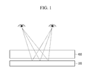
- FIGS. 1 and 2 are schematic views illustrating a configuration of an image display device according to an exemplary embodiment and methods of forming a 2D image and a 3D image, respectively.
- an image display device includes a display panel 300 displaying images, and a diffractive element 400 positioned in front of an image display surface of the display panel 300.
- the display panel 300 and the diffractive element 400 may operate in a 2D mode or a 3D mode.
- the display panel 300 may be any one of various types of flat panel displays, such as a plasma display panel (PDP), a liquid crystal display (LCD), an organic light emitting diode (OLED) display, etc.
- the display panel 300 includes a plurality of pixels PX which are arranged in a matrix and display an image.
- the display panel 300 displays one 2D image.
- the display panel 300 may alternately display images corresponding to various visual fields, such as right eye images, left eye images, etc., by a space or time division method.
- the display panel 300 may alternately display right eye images and left eye images every other pixel column in the 3D mode.
- the diffractive element 400 transmits an image displayed on the display panel 300 as it is, but in the 3D mode, it divides visual fields of the image of display panel 300. That is, the diffractive element 400 operating in the 3D mode focuses multiple viewpoint images, including the left eye image and the right eye image displayed on the display panel 300, on visual fields corresponding to each viewpoint image by using the diffraction and refraction phenomenon of light.
- FIG. 1 shows a case where the display panel 300 and the diffractive element 400 operate in the 2D mode in which the same image reaches the left eye and the right eye such that a 2D image is perceived
- FIG. 2 shows a case where the display panel 300 and the diffractive element 400 operate in the 3D mode in which the diffractive element 400 divides an image including an image for left eye and an image for right eye of the display panel 300 into individual visual fields such as the left eye and the right eye and diffracts the image such that a 3D image is perceived.
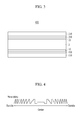
- FIG. 3 is an example of a cross-sectional view of the diffractive element of the image display device according to the exemplary embodiment.
- the diffractive element 400 includes a first substrate 110 and a second substrate 210 facing each other, and a liquid crystal layer 3 interposed between the two substrates 110 and 210.
- the first substrate 110 and the second substrate 210 are made of an insulating material such as glass, plastic, etc.
- polarizers On outside surfaces of the substrates 110 and 210, polarizers (not shown) may be provided.
- first electrode layer 190 and an alignment layer 11 are sequentially formed, and on the second substrate 210, a second electrode layer 290 and an alignment layer 21 are sequentially formed.
- the first electrode layer 190 and the second electrode layer 290 include a plurality of electrodes and may be made of a transparent conductive material such as ITO (indium tin oxide) or IZO(indium zinc oxide).
- ITO indium tin oxide
- IZO indium zinc oxide
- the alignment layers 11 and 21 determine the initial alignment of the liquid crystal molecules of the liquid crystal layer 3. Because the alignment layers 11 and 21 determine the arrangement direction of the liquid crystal molecules before voltages are applied, once voltages are applied, the liquid crystal molecules are quickly arranged according to the electric field formed in the liquid crystal layer 3.
- the liquid crystal layer 3 may be aligned in various modes such as a horizontal alignment mode, a vertical alignment mode, TN (twisted nematic) mode, etc.
- the diffractive element 400 operates in the 2D mode or the 3D mode according to voltages applied to the first electrode layer 190 and the second electrode layer 290. For example, when voltages are not applied to the first electrode layer 190 and the second electrode layer 290, the diffractive element 400 may operate in the 2D mode. When, on the other hand, voltages are applied to the first electrode layer 190 and the second electrode layer 290, the diffractive element 400 may operate in the 3D mode. To this end, the initial orientation direction of the liquid crystal molecules and the transmissive axis directions of the polarizers may be appropriately adjusted.
- the diffractive element 400 operating in the 3D mode includes a plurality of unit lenses.
- the plurality of unit lenses may be repeatedly arranged in one side direction of the diffractive element 400 at predetermined intervals.
- the positions of the unit lenses in the diffractive element 400 may be fixed or vary with time.
- Each unit lens may be implemented as a Fresnel zone plate.
- a Fresnel zone plate is a device functioning as a lens by using a plurality of concentric circles which are radially arranged and in which intervals therebetween decrease from the center to the outside, as Fresnel zones.
- a Fresnel zone plate uses the diffraction phenomenon of light, instead of the refraction phenomenon of light, to focus light.
- FIG. 4 is a graph illustrating, for a phase modulation type of Fresnel zone plate, changes in phase delay according to the position along the plate.
- each zone of the Fresnel zone plate is an area in which each repeated waveform in the graph is located.
- each zone the phase delay changes in a step-wise fashion.
- the phase delay changes in two stages.
- the phase delay changes in four stages.
- FIG. 4 is not intended to limit the number of stages in which the phase delay changes, and various numbers of stages may be used.
- the Fresnel zone plate shown in FIG. 4 in which the phase delay in each zone changes in the step-wise fashion, is referred to a multi-level phase modulation zone plate.
- the diffractive element diffracts light passing through the individual zones, and through the diffraction and the destructive and constructive interference of the light, it is focused.
- it is possible to create a lens effect by forming a phase delay distribution according to the Fresnel zone plate for each unit lens of the diffractive element 400.
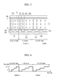
- FIG. 5 is a cross-sectional view illustrating a portion of a unit lens of the diffractive element 400 according to the exemplary embodiment.
- the identical components with those in the exemplary embodiment of FIG. 3 are denoted by the same reference numerals, and the same description is omitted.
- the diffractive element 400 includes the first substrate 110 and the second substrate 210 facing each other, and the liquid crystal layer 3 interposed between the two substrates 110 and 210.
- the first electrode layer 190 and the alignment layer 11 are sequentially formed, and on the second substrate 210, the second electrode layer 290 and the alignment layer 21 are sequentially formed.
- the first electrode layer 190 includes a first electrode array 191 including a plurality of first electrodes 193, an insulating layer 180 formed on the first electrode array 191, and a second electrode array 195 formed on the insulating layer 180 and including a plurality of second electrodes 197.
- the first electrodes 193 and the second electrodes 197 may be alternately positioned in a horizontal direction and may be arranged so that they do not overlap each other.
- FIG. 5 shows that the edges of the first electrodes 193 and the second electrodes 197 neighboring each other do not overlap each other, however, the edges may partially overlap each other.
- the horizontal widths of the first electrodes 193 and the second electrodes 197, the horizontal intervals between the first electrodes 193, and the horizontal intervals between the second electrodes 197 gradually decrease from the center of the unit lens to the outside of the unit lens, becoming smaller in the individual zones that are farther from the center.
- each zone of the unit lens such as the (n-1)-th zone, the n-th zone, and the (n+1)-th zone illustrated in FIG. 5 .
- two first electrodes 193 and two second electrodes 197 are positioned.
- An area in each zone where each of the electrodes 193 and 197 is positioned forms a subzone, such as subzones sZ1, sZ2, sZ3, or sZ4.
- FIG. 5 shows one zone including four subzones sZ1, sZ2, sZ3, and sZ4, but the number of subzones is not limited thereto. Also, unlike what is shown in FIG. 5 , the horizontal widths of the first electrodes 193 and the second electrodes 197 included in one zone may be constant, and the numbers of electrodes 193 and 197 included in the individual zones may decrease toward the outermost zone.
- the horizontal widths of the first electrodes 193 and the second electrodes 197 may be greater than or equal to a cell gap of the liquid crystal layer 3.
- the amount that the cell gap may be reduced is limited, due to process limitations and limitations imposed by the refractive index of the liquid crystal.
- the insulating layer 180 may be made of an inorganic material, an organic material, etc., and electrically insulates the first electrode array 191 and the second electrode array 195 from each other.
- the second electrode layer 290 is formed on the entire surface of the second substrate 210 and receives a predetermined voltage such as a common voltage Vcom, etc.
- the second electrode layer 290 may be made of a transparent conductive material such as ITO, IZO, etc.
- the alignment layers 11 and 21 may be rubbed in a longitudinal direction perpendicular to the width (horizontal) direction of the first electrode 193 and the second electrode 197 (a direction perpendicular to the plane of FIG. 5 ) or in a direction forming a predetermined angle with the width (horizontal direction.
- the rubbed directions of the alignment layer 11 and the alignment layer 21 may be opposite to each other.
- the liquid crystal molecules 31 of the liquid crystal layer 3 may be initially aligned, before application of an electric field, in a direction parallel to the surfaces of the substrates 110 and 210, but the alignment mode of the liquid crystal layer 3 is not limited thereto. Vertical alignment and other alignment modes are possible.
- FIG. 6 is a view illustrating the phase delay which should be achieved according to position in the diffractive element of FIG. 5 .
- each unit lens of the diffractive element is implemented as the phase modulation type of Fresnel zone plate.
- the phase delay changes in four stages.
- the phase delay increases in the step-wise fashion from the outside to the center (as shown in FIG. 4 ).
- the same subzones of the plurality of zones cause the same phase delay.
- the slope of the phase delay with respect to the base of the lens unit is vertical.
- phase delays according to the position in the diffractive element, voltages applied to the diffractive element are adjusted. However, it is difficult to make the slope of the phase delay vertical at the zone boundaries. In particular, it is difficult to control the phase delay at a zone boundary portion.
- the cell gap of the liquid crystal layer should be reduced. However, the amount that the cell gap may be reduced is limited, due to process limitations and limitations imposed by the refractive index of the liquid crystal.
- FIG. 7 is a view illustrating examples of voltages applied to the first electrode layer 190 of a diffractive element 400 in an image display device according to a first exemplary embodiment
- FIG. 8 is a view illustrating examples of voltages applied to a first electrode layer 190 of a diffractive element 400 in an image display device according to a second exemplary embodiment
- FIG. 9 is a view illustrating electric fields formed in the diffractive element when the voltages are applied to the first electrode layer 190 of the diffractive element 400 as in FIG. 8
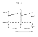
- FIG. 10 is a view illustrating a phase delay and transmittance according to the position in the diffractive element 400 of FIG. 9 .
- the identical components with those in the exemplary embodiment of FIG. 5 are denoted by the same reference numerals, and redundant description is omitted.
- voltages having positive polarity with respect to the common voltage Vcom are applied to the n-th zone of the unit lens of the diffractive element, and voltages having negative polarity with respect to the common voltage Vcom are applied to the (n-1)-th zone of the unit lens.
- the common voltage Vcom is applied to the second electrode layer 290 of the diffractive element (see FIG. 5 ).
- the polarity of the voltages applied to the first electrode layer 190 with respect to the common voltage Vcom (hereinafter, "the polarity of the voltages applied to the first electrode layer with respect to the common voltage” is simply referred to as “the polarity of the voltages applied to the first electrode layer”) is inverted every zone. Such inversion of the polarity of the voltages is referred to as a spatial inversion of the polarity of the voltage.
- a temporal inversion of the polarity of the voltage may occur with the spatial inversion, so a positive voltage changes periodically to a negative voltage and a negative voltage changes periodically to a positive voltage.
- the first electrode layer 190 of each zone receives step-wise voltages in which the differences from the common voltage Vcom gradually decrease from the outside to the center within each zone.
- voltages applied to the subzones sZ1, sZ2, sZ3, and sZ4 of the n-th zone and the (n-1)-th zone are denoted by reference symbols V1, ..., and V8 in order from the outside to the center.
- the voltages V1 to V8 can satisfy the following Equation with respect to the common voltage Vcom.
- P ⁇ V ⁇ 1 - Vcom P ⁇ V ⁇ 5 - Vcom
- P ⁇ V ⁇ 2 - Vcom P ⁇ V ⁇ 6 - Vcom
- P ⁇ V ⁇ 3 - Vcom P ⁇ V ⁇ 7 - Vcom
- P ⁇ V ⁇ 4 - Vcom P ⁇ V ⁇ 8 - Vcom
- P(V) means the phase delay which light of a specific single wavelength vertically incident to the liquid crystal layer undergoes when passing through the liquid crystal layer at the position of that electrode when voltage, which is the voltage difference between the electrode and the common electrode, is applied.
- the phase change of the light is due to realignment of liquid crystal molecules on each electrode as the result of the voltage difference between the electrode and the common electrode.
- Voffset V4-Vcom or Vcom-V8
- Voffset V4-Vcom or Vcom-V8
- the offset voltage Voffset is 0.
- the offset voltage Voffset can be adjusted as FIG. 8 , and the offset voltage Voffset may differ according to the positions of the zones even in one unit lens.
- electric fields are formed between the first electrode layer 190 and the second electrode layer 290, and an electric field is formed between two electrodes adjacent to the zone boundary.
- the intensities of the electric fields formed between the first electrode layer 190 and the second electrode layer 290 decrease from the outside to the center (as represented by fewer arrows as the intensity of the electric field decreases) . This is because the differences between the voltages applied to the first electrode layer 190 and the common voltage Vcom decrease from the outside to the center.
- a first electrode 193 of the n-th zone closest to the center forms a first electric field E1 together with an adjacent second electrode of the n-th zone, forms a second electric field E2 together with the second electrode layer 290, and forms a third electric field E3 together with an adjacent second electrode 197 of the (n-1)-th zone.
- the intensity of the third electric field E3 is higher than the intensities of the other electric fields E1 and E2.
- the diffractive element can form a phase delay distribution according to the Fresnel zone plate so as to create a lens effect.
- the slope of the phase delay at the zone boundaries is vertical.
- the slope of the phase delay at a zone boundary portion ZG is not vertical. Because it is difficult to control the phase delay in the zone boundary ZG, in the zone boundary portion ZG, the phase delay which should be achieved for a lens function is not properly implemented.
- the polarity of the voltages to the first electrode layer 190 is inverted every zone as shown in FIG. 8 , such that the electric field E3 is formed at the boundary of zones adjacent to each other and the liquid crystal molecules of the liquid crystal layer 3 are aligned according to the electric field E3, so as to reduce the transmittance in the zone boundary portion ZG.
- the voltage difference dV between the voltages applied two electrodes adjacent to each other at the zone boundary may be set so that the transmittance of the zone boundary portion ZG is equal to or less than a predetermined value.
- the transmittance reduction can act as amplitude grating. However, because degradation of lens characteristics caused by a phase control defect is greater than an amplitude grating effect, as the transmittance of the zone boundary portion ZG is reduced, diffraction efficiency can increase.
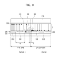
- FIG. 11 is a view illustrating electric fields formed in the diffractive element in the image display device according to another exemplary embodiment
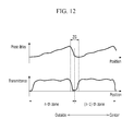
- FIG. 12 is a view illustrating a phase delay and transmittance according to the position in the diffractive element in the case of FIG. 11 .
- Identical components with those of the previous exemplary embodiment are denoted by the same reference numerals, and repetitive description is omitted.
- a unit lens according to the exemplary embodiment of FIG. 11 is almost the same as the unit lens shown in FIG. 9 , but is different from that shown in FIG. 9 in the configuration of the first electrode layer 190.
- the first electrode layer 190 in each zone, includes four electrodes. However, in FIG. 11 , in each zone, the first electrode layer 190 includes three electrodes.
- the first electrode layer 190 includes a first electrode array 191 including a plurality of first electrodes 194, an insulating layer 180 formed on the first electrode array 191, and a second electrode array 195 formed on the insulating layer 180 and including a plurality of second electrodes 198.
- the polarity of the voltages applied to the first electrode layer 190 is inverted every zone as described above with respect to FIGS. 7 and 8 .
- the first electrode layer 190 of each zone receives step-wise voltages in which the differences from the common voltage Vcom gradually decrease from the outside to the center. Voltages may be applied to electrodes corresponding to the same subzone for individual zones so that the phase delays at corresponding portions of the liquid crystal layer are the same.
- the edges of the first electrode 194 and the second electrode 198 adjacent to each other may be arranged so as to not overlap each other.
- An interval d between two electrodes adjacent to each other at a zone boundary may increase as compared to the case of FIG. 9 .
- an electrode interval D which is the interval between the first electrodes 194 or the interval between the second electrodes 198 may also increase as compared to the case of FIG. 9 .
- An interval d between two electrodes adjacent to each other at a zone boundary, the electrode interval D, and the cell gap may be set so that a phase delay distribution necessary for a lens function of the diffractive element is formed while the transmittance of the zone boundary portion is equal to or less than a predetermined value.
- the diffractive element in each zone, the phase delay increases from the outside to the center. Therefore, the diffractive element can form a phase delay distribution according to the Fresnel zone plate so as to create a lens effect.
- the slope of the phase delay is not vertical at the zone boundary portion ZG. Because it is difficult to control the phase delay in the zone boundary ZG, in the zone boundary portion ZG, the phase delay which should be achieved for a lens function is not properly implemented. Because the polarity of the voltages applied to the first electrode layer 190 is inverted every zone as shown in FIG. 11 , an electric field is formed at the boundary of zones adjacent to each other and the liquid crystal molecules of the liquid crystal layer 3 are aligned in a direction perpendicular to the electric field, so as to reduce the transmittance in the zone boundary portion ZG.
- an image display device capable of reducing the transmittance of the zone boundary portion and improving lens characteristics by inverting the polarity of the voltages every zone.
- Voffset is the difference between the center side voltage applied to the electrode of each zone closest to the center and the common voltage.
- Voffset the difference between the center side voltage applied to the electrode of each zone closest to the center and the common voltage.
- Voffset is the difference between the center side voltage applied to the electrode of each zone closest to the center and the common voltage.
- the degree of horizontal rotation of a director of the liquid crystal is controlled by controlling the voltage difference dV between the voltages applied to two electrodes adjacent to each other at the zone boundary. Because the transmittance of the diffractive element is influenced by the degree of horizontal rotation of the director of the liquid crystal, the transmittance of the zone boundary portion can be adjusted. This makes it possible to improve the liquid crystal lens characteristic of the diffractive element 400.
- the phase delay distribution and the transmittance of the zone boundary portion are simultaneously determined by the cell gap and the voltages applied to the diffractive element.
Landscapes
- Physics & Mathematics (AREA)
- Optics & Photonics (AREA)
- General Physics & Mathematics (AREA)
- Nonlinear Science (AREA)
- Signal Processing (AREA)
- Engineering & Computer Science (AREA)
- Multimedia (AREA)
- Crystallography & Structural Chemistry (AREA)
- Chemical & Material Sciences (AREA)
- Mathematical Physics (AREA)
- Geometry (AREA)
- Liquid Crystal (AREA)
- Testing, Inspecting, Measuring Of Stereoscopic Televisions And Televisions (AREA)
- Stereoscopic And Panoramic Photography (AREA)
- Devices For Indicating Variable Information By Combining Individual Elements (AREA)
Applications Claiming Priority (1)
| Application Number | Priority Date | Filing Date | Title |
|---|---|---|---|
| KR1020100136966A KR101707587B1 (ko) | 2010-12-28 | 2010-12-28 | 회절 소자를 이용한 영상 표시 장치 |
Publications (2)
| Publication Number | Publication Date |
|---|---|
| EP2472885A2 true EP2472885A2 (fr) | 2012-07-04 |
| EP2472885A3 EP2472885A3 (fr) | 2015-03-18 |
Family
ID=45747006
Family Applications (1)
| Application Number | Title | Priority Date | Filing Date |
|---|---|---|---|
| EP11174907.3A Withdrawn EP2472885A3 (fr) | 2010-12-28 | 2011-07-21 | Dispositif d'affichage d'images utilisant un élément diffractif |
Country Status (5)
| Country | Link |
|---|---|
| US (2) | US9256075B2 (fr) |
| EP (1) | EP2472885A3 (fr) |
| JP (1) | JP5877979B2 (fr) |
| KR (1) | KR101707587B1 (fr) |
| CN (1) | CN102566064B (fr) |
Cited By (2)
| Publication number | Priority date | Publication date | Assignee | Title |
|---|---|---|---|---|
| US9664912B2 (en) | 2013-02-13 | 2017-05-30 | Samsung Display Co., Ltd. | Image display and liquid crystal lens therefor |
| US10197880B2 (en) | 2016-06-17 | 2019-02-05 | Boe Technology Group Co., Ltd. | Liquid crystal lens, display device and driving method thereof |
Families Citing this family (38)
| Publication number | Priority date | Publication date | Assignee | Title |
|---|---|---|---|---|
| KR101698571B1 (ko) * | 2010-10-29 | 2017-02-02 | 삼성디스플레이 주식회사 | 회절 소자를 이용한 영상 표시 장치 |
| JP5599420B2 (ja) * | 2012-03-22 | 2014-10-01 | 株式会社東芝 | 液晶フレネルレンズ素子及び画像表示装置 |
| KR101923150B1 (ko) * | 2012-04-16 | 2018-11-29 | 삼성디스플레이 주식회사 | 표시 장치 및 이를 이용한 입체 영상 표시 방법 |
| KR101476884B1 (ko) * | 2012-06-22 | 2014-12-26 | 엘지디스플레이 주식회사 | 패럴랙스 배리어 타입의 입체영상 표시장치 |
| US20160277726A1 (en) * | 2012-08-30 | 2016-09-22 | 3Nd Technology Limited | Multi-purpose eyewear article |
| US20140063376A1 (en) * | 2012-08-30 | 2014-03-06 | 3Nd Technology Limited | Liquid-crystal optical modules and multi-purpose eyewear using the same |
| KR20140053741A (ko) * | 2012-10-26 | 2014-05-08 | 삼성디스플레이 주식회사 | 액정 렌즈, 이를 포함하는 액정 모듈 및 액정 모듈의 구동 방법 |
| CN104297929B (zh) * | 2013-07-19 | 2017-02-08 | 华为技术有限公司 | 立体成像的装置、方法和显示器 |
| KR20150045135A (ko) * | 2013-10-18 | 2015-04-28 | 삼성디스플레이 주식회사 | 입체영상 표시장치와 그 구동방법 |
| KR20150047967A (ko) * | 2013-10-25 | 2015-05-06 | 삼성디스플레이 주식회사 | 표시 장치 및 그 구동 방법 |
| KR102134904B1 (ko) | 2013-10-30 | 2020-07-17 | 삼성디스플레이 주식회사 | 3차원 표시 장치 및 3차원 표시 장치용 액정 렌즈부 |
| KR102114757B1 (ko) * | 2013-11-05 | 2020-05-26 | 삼성디스플레이 주식회사 | 영상 표시 장치 |
| KR20150054212A (ko) * | 2013-11-11 | 2015-05-20 | 삼성디스플레이 주식회사 | 표시 장치 및 이를 위한 액정 렌즈 패널 장치 |
| CN104007554A (zh) * | 2013-11-25 | 2014-08-27 | 深圳市亿思达显示科技有限公司 | 一种动态光栅装置 |
| CN104656321B (zh) * | 2013-11-25 | 2023-07-07 | 深圳市维超智能科技有限公司 | 一种动态光栅装置 |
| KR20150061967A (ko) * | 2013-11-28 | 2015-06-05 | 삼성디스플레이 주식회사 | 표시장치 |
| KR20150066363A (ko) | 2013-12-06 | 2015-06-16 | 삼성디스플레이 주식회사 | 액정 렌즈 모듈 |
| KR20150070784A (ko) * | 2013-12-17 | 2015-06-25 | 삼성디스플레이 주식회사 | 액정 프레넬 렌즈 및 그 제조 방법 |
| KR102141555B1 (ko) * | 2013-12-24 | 2020-08-05 | 엘지디스플레이 주식회사 | 입체 영상 표시 장치 및 이의 구동 방법 |
| KR102188512B1 (ko) | 2014-02-03 | 2020-12-09 | 삼성디스플레이 주식회사 | 입체 영상 표시 장치 및 입체 영상 표시 장치용 액정 렌즈 패널 |
| KR102192590B1 (ko) * | 2014-02-04 | 2020-12-18 | 삼성디스플레이 주식회사 | 표시 장치 및 이의 구동 방법 |
| KR102120422B1 (ko) * | 2014-02-05 | 2020-06-09 | 삼성디스플레이 주식회사 | 렌즈를 포함하는 표시 장치 |
| KR102192207B1 (ko) * | 2014-04-29 | 2020-12-18 | 삼성디스플레이 주식회사 | 영상 표시 장치 |
| KR20150139695A (ko) | 2014-06-03 | 2015-12-14 | 삼성디스플레이 주식회사 | 액정 렌즈 장치 및 이를 포함하는 표시 장치 |
| JP2016018126A (ja) * | 2014-07-09 | 2016-02-01 | 株式会社東芝 | 液晶レンズ装置及び画像表示装置 |
| KR102230549B1 (ko) | 2014-09-12 | 2021-03-22 | 삼성디스플레이 주식회사 | 접촉 감지 기능을 가진 광학계 및 이를 포함하는 표시 장치 |
| CN104317133A (zh) * | 2014-11-12 | 2015-01-28 | 京东方科技集团股份有限公司 | 液晶透镜及显示装置 |
| KR20160066658A (ko) * | 2014-12-02 | 2016-06-13 | 삼성디스플레이 주식회사 | 광 변조 장치 및 그 구동 방법 |
| KR102293125B1 (ko) | 2015-01-08 | 2021-08-24 | 삼성디스플레이 주식회사 | 접촉 감지 기능을 가진 광학계 및 이를 포함하는 표시 장치 |
| KR102323453B1 (ko) * | 2015-01-12 | 2021-11-08 | 삼성디스플레이 주식회사 | 액정을 포함한 광 변조 장치, 그 구동 방법 및 이를 이용한 광학 표시 장치 |
| JP6573467B2 (ja) * | 2015-03-31 | 2019-09-11 | 株式会社ジャパンディスプレイ | 画像表示装置及び液晶パネル |
| JP6514938B2 (ja) * | 2015-03-31 | 2019-05-15 | 株式会社ジャパンディスプレイ | 画像表示装置及び液晶パネル |
| CN105607379A (zh) * | 2016-03-16 | 2016-05-25 | 京东方科技集团股份有限公司 | 液晶透镜及其驱动方法、显示装置 |
| JP6284208B1 (ja) * | 2016-12-19 | 2018-02-28 | 国立大学法人秋田大学 | 液晶レンズアレイ |
| KR102394802B1 (ko) * | 2017-10-11 | 2022-05-04 | 현대자동차주식회사 | 운송 수단용 고분자 분산형 액정 필름 및 이를 포함하는 운송 수단 |
| CN110286529B (zh) * | 2018-03-19 | 2021-04-06 | 京东方科技集团股份有限公司 | 液晶盒及其驱动方法和液晶镜片 |
| KR102648614B1 (ko) | 2018-10-04 | 2024-03-19 | 삼성디스플레이 주식회사 | 표시 장치 |
| TWI885630B (zh) * | 2023-12-08 | 2025-06-01 | 宏碁股份有限公司 | 顯示裝置 |
Citations (1)
| Publication number | Priority date | Publication date | Assignee | Title |
|---|---|---|---|---|
| US20080252720A1 (en) * | 2007-04-12 | 2008-10-16 | Samsung Electronics Co., Ltd. | Highly efficient 2d-3d switchable display device |
Family Cites Families (15)
| Publication number | Priority date | Publication date | Assignee | Title |
|---|---|---|---|---|
| JP3401760B2 (ja) | 1997-11-04 | 2003-04-28 | 日本電信電話株式会社 | 光学装置 |
| KR100440956B1 (ko) | 2001-09-11 | 2004-07-21 | 삼성전자주식회사 | 2d/3d 겸용 디스플레이 |
| JP4349781B2 (ja) | 2002-09-10 | 2009-10-21 | パイオニア株式会社 | 液晶レンズ並びにその駆動方法及び装置 |
| JP4436070B2 (ja) | 2003-05-09 | 2010-03-24 | シチズンホールディングス株式会社 | 液晶光学素子及び光学装置 |
| US8885139B2 (en) * | 2005-01-21 | 2014-11-11 | Johnson & Johnson Vision Care | Adaptive electro-active lens with variable focal length |
| JP2006259058A (ja) | 2005-03-16 | 2006-09-28 | Matsushita Electric Ind Co Ltd | 三次元画像表示装置 |
| US7775666B2 (en) | 2005-03-16 | 2010-08-17 | Panasonic Corporation | Three-dimensional image communication terminal and projection-type three-dimensional image display apparatus |
| KR101201848B1 (ko) | 2006-02-20 | 2012-11-15 | 삼성디스플레이 주식회사 | 입체영상 변환패널 및 이를 갖는 입체영상 표시장치 |
| US8614782B2 (en) | 2006-06-27 | 2013-12-24 | Lg Display Co., Ltd. | Liquid crystal lens and image display device including the same |
| JP2008216626A (ja) * | 2007-03-05 | 2008-09-18 | Citizen Holdings Co Ltd | 可変焦点レンズ |
| KR20090004006A (ko) | 2007-07-06 | 2009-01-12 | 엘지디스플레이 주식회사 | 액정렌즈 |
| KR101222990B1 (ko) * | 2007-10-22 | 2013-01-18 | 엘지디스플레이 주식회사 | 액정 전계 렌즈 및 이를 이용한 입체 표시 장치 |
| WO2009072670A1 (fr) | 2007-12-06 | 2009-06-11 | Citizen Holdings Co., Ltd. | Lentille de fresnel à cristaux liquides |
| KR101472052B1 (ko) | 2008-07-30 | 2014-12-12 | 삼성디스플레이 주식회사 | 표시장치 |
| KR101772153B1 (ko) | 2010-03-17 | 2017-08-29 | 삼성디스플레이 주식회사 | 회절 렌즈를 이용한 영상 표시 장치 |
-
2010
- 2010-12-28 KR KR1020100136966A patent/KR101707587B1/ko not_active Expired - Fee Related
-
2011
- 2011-07-21 EP EP11174907.3A patent/EP2472885A3/fr not_active Withdrawn
- 2011-07-28 US US13/193,104 patent/US9256075B2/en not_active Expired - Fee Related
- 2011-09-20 JP JP2011204768A patent/JP5877979B2/ja not_active Expired - Fee Related
- 2011-10-24 CN CN201110326250.0A patent/CN102566064B/zh not_active Expired - Fee Related
-
2016
- 2016-01-11 US US14/992,737 patent/US9823483B2/en not_active Expired - Fee Related
Patent Citations (1)
| Publication number | Priority date | Publication date | Assignee | Title |
|---|---|---|---|---|
| US20080252720A1 (en) * | 2007-04-12 | 2008-10-16 | Samsung Electronics Co., Ltd. | Highly efficient 2d-3d switchable display device |
Cited By (3)
| Publication number | Priority date | Publication date | Assignee | Title |
|---|---|---|---|---|
| US9664912B2 (en) | 2013-02-13 | 2017-05-30 | Samsung Display Co., Ltd. | Image display and liquid crystal lens therefor |
| US10036894B2 (en) | 2013-02-13 | 2018-07-31 | Samsung Display Co., Ltd. | Image display and liquid crystal lens therefor |
| US10197880B2 (en) | 2016-06-17 | 2019-02-05 | Boe Technology Group Co., Ltd. | Liquid crystal lens, display device and driving method thereof |
Also Published As
| Publication number | Publication date |
|---|---|
| US9823483B2 (en) | 2017-11-21 |
| KR101707587B1 (ko) | 2017-02-17 |
| JP5877979B2 (ja) | 2016-03-08 |
| US20120162550A1 (en) | 2012-06-28 |
| US20160124237A1 (en) | 2016-05-05 |
| US9256075B2 (en) | 2016-02-09 |
| JP2012141575A (ja) | 2012-07-26 |
| CN102566064B (zh) | 2016-11-23 |
| CN102566064A (zh) | 2012-07-11 |
| KR20120074966A (ko) | 2012-07-06 |
| EP2472885A3 (fr) | 2015-03-18 |
Similar Documents
| Publication | Publication Date | Title |
|---|---|---|
| EP2472885A2 (fr) | Dispositif d'affichage d'images utilisant un élément diffractif | |
| US8605227B2 (en) | Image display device using diffractive device | |
| JP5596625B2 (ja) | 表示装置 | |
| JP5907653B2 (ja) | 回折レンズを利用した画像表示装置 | |
| US9164285B2 (en) | Three-dimensional image display apparatus | |
| US10036894B2 (en) | Image display and liquid crystal lens therefor | |
| KR20130060637A (ko) | 2차원/3차원 전환 가능한 디스플레이 장치 | |
| CN103257486B (zh) | 显示装置 | |
| EP2881786B1 (fr) | Module de lentille à cristaux liquides | |
| US9442298B2 (en) | Liquid crystal display panel and method for manufacturing the same | |
| TWI467245B (zh) | 顯示裝置及液晶透鏡 | |
| KR102371780B1 (ko) | 액정 렌즈 패널 및 이를 구비하는 표시 장치 | |
| US9759925B2 (en) | Three-dimensional image display apparatus | |
| US9557570B2 (en) | Display device and liquid crystal lens panel for the same | |
| US20160195739A1 (en) | Display device and liquid crystal lens panel | |
| US9658483B2 (en) | Liquid crystal lens and display including the same | |
| US9420267B2 (en) | Display device and liquid crystal lens panel device for the same | |
| KR20160110667A (ko) | 액정 렌즈 및 이를 포함하는 표시 장치 | |
| US9235081B2 (en) | Display device including lens | |
| US9726942B2 (en) | Liquid crystal lens panel | |
| US20150131012A1 (en) | Display device and liquid crystal lens panel device for the same |
Legal Events
| Date | Code | Title | Description |
|---|---|---|---|
| 17P | Request for examination filed |
Effective date: 20120328 |
|
| AK | Designated contracting states |
Kind code of ref document: A2 Designated state(s): AL AT BE BG CH CY CZ DE DK EE ES FI FR GB GR HR HU IE IS IT LI LT LU LV MC MK MT NL NO PL PT RO RS SE SI SK SM TR |
|
| AX | Request for extension of the european patent |
Extension state: BA ME |
|
| PUAI | Public reference made under article 153(3) epc to a published international application that has entered the european phase |
Free format text: ORIGINAL CODE: 0009012 |
|
| RAP1 | Party data changed (applicant data changed or rights of an application transferred) |
Owner name: SAMSUNG ELECTRONICS CO., LTD. |
|
| RAP1 | Party data changed (applicant data changed or rights of an application transferred) |
Owner name: SAMSUNG DISPLAY CO., LTD. |
|
| PUAL | Search report despatched |
Free format text: ORIGINAL CODE: 0009013 |
|
| AK | Designated contracting states |
Kind code of ref document: A3 Designated state(s): AL AT BE BG CH CY CZ DE DK EE ES FI FR GB GR HR HU IE IS IT LI LT LU LV MC MK MT NL NO PL PT RO RS SE SI SK SM TR |
|
| AX | Request for extension of the european patent |
Extension state: BA ME |
|
| RIC1 | Information provided on ipc code assigned before grant |
Ipc: G02B 5/18 20060101ALI20150212BHEP Ipc: G02F 1/1335 20060101ALI20150212BHEP Ipc: H04N 13/04 20060101AFI20150212BHEP |
|
| RAP1 | Party data changed (applicant data changed or rights of an application transferred) |
Owner name: SAMSUNG DISPLAY CO., LTD. |
|
| 17Q | First examination report despatched |
Effective date: 20170110 |
|
| STAA | Information on the status of an ep patent application or granted ep patent |
Free format text: STATUS: THE APPLICATION IS DEEMED TO BE WITHDRAWN |
|
| 18D | Application deemed to be withdrawn |
Effective date: 20170802 |