EP2473654B1 - Verfahren zur elektrochemischen verarbeitung von unebenen proben - Google Patents
Verfahren zur elektrochemischen verarbeitung von unebenen proben Download PDFInfo
- Publication number
- EP2473654B1 EP2473654B1 EP10737059.5A EP10737059A EP2473654B1 EP 2473654 B1 EP2473654 B1 EP 2473654B1 EP 10737059 A EP10737059 A EP 10737059A EP 2473654 B1 EP2473654 B1 EP 2473654B1
- Authority
- EP
- European Patent Office
- Prior art keywords
- sample
- carrying element
- fixing element
- carrying
- electrical contact
- Prior art date
- Legal status (The legal status is an assumption and is not a legal conclusion. Google has not performed a legal analysis and makes no representation as to the accuracy of the status listed.)
- Not-in-force
Links
Images



Classifications
-
- C—CHEMISTRY; METALLURGY
- C25—ELECTROLYTIC OR ELECTROPHORETIC PROCESSES; APPARATUS THEREFOR
- C25F—PROCESSES FOR THE ELECTROLYTIC REMOVAL OF MATERIALS FROM OBJECTS; APPARATUS THEREFOR
- C25F7/00—Constructional parts, or assemblies thereof, of cells for electrolytic removal of material from objects; Servicing or operating
-
- C—CHEMISTRY; METALLURGY
- C25—ELECTROLYTIC OR ELECTROPHORETIC PROCESSES; APPARATUS THEREFOR
- C25D—PROCESSES FOR THE ELECTROLYTIC OR ELECTROPHORETIC PRODUCTION OF COATINGS; ELECTROFORMING; APPARATUS THEREFOR
- C25D17/00—Constructional parts, or assemblies thereof, of cells for electrolytic coating
- C25D17/005—Contacting devices
-
- C—CHEMISTRY; METALLURGY
- C25—ELECTROLYTIC OR ELECTROPHORETIC PROCESSES; APPARATUS THEREFOR
- C25D—PROCESSES FOR THE ELECTROLYTIC OR ELECTROPHORETIC PRODUCTION OF COATINGS; ELECTROFORMING; APPARATUS THEREFOR
- C25D17/00—Constructional parts, or assemblies thereof, of cells for electrolytic coating
- C25D17/06—Suspending or supporting devices for articles to be coated
- C25D17/08—Supporting racks, i.e. not for suspending
-
- C—CHEMISTRY; METALLURGY
- C25—ELECTROLYTIC OR ELECTROPHORETIC PROCESSES; APPARATUS THEREFOR
- C25D—PROCESSES FOR THE ELECTROLYTIC OR ELECTROPHORETIC PRODUCTION OF COATINGS; ELECTROFORMING; APPARATUS THEREFOR
- C25D7/00—Electroplating characterised by the article coated
-
- H—ELECTRICITY
- H10—SEMICONDUCTOR DEVICES; ELECTRIC SOLID-STATE DEVICES NOT OTHERWISE PROVIDED FOR
- H10P—GENERIC PROCESSES OR APPARATUS FOR THE MANUFACTURE OR TREATMENT OF DEVICES COVERED BY CLASS H10
- H10P72/00—Handling or holding of wafers, substrates or devices during manufacture or treatment thereof
- H10P72/04—Apparatus for manufacture or treatment
- H10P72/0402—Apparatus for fluid treatment
- H10P72/0418—Apparatus for fluid treatment for etching
- H10P72/0422—Apparatus for fluid treatment for etching for wet etching
- H10P72/0426—Apparatus for fluid treatment for etching for wet etching with the semiconductor substrates being dipped in baths or vessels
Definitions
- This invention relates to methods and systems for electrochemical processing of non-flat samples and/or samples that may change shape during electrochemical processing. More in particular it relates to methods and systems for holding such samples and for maintaining a good electrical contact to such samples during electrochemical processing, e.g. electrochemical etching, plating or cleaning.
- a wafering technique is described that enables the production of very thin (e.g. thinner than 100 micrometer) crystalline silicon wafers. This process is also known as the SLIM-Cut (Stress-induced Lift-off Method) process.
- SLIM-Cut Stress-induced Lift-off Method
- a layer e.g. a metallic layer with mismatched thermal expansion coefficient with respect to the mother substrate is provided, e.g. screen printed.
- the thermal coefficient of expansion of the metallic layer is much higher, e.g. more than a factor of 10 higher, than the thermal coefficient of expansion of silicon.
- Good bonding between the metallic layer and the silicon mother substrate can for example be achieved by a treatment at high temperature in a belt furnace. Upon cooling to room temperature, the metallic layer and the silicon substrate undergo a thermal contraction, and the mismatch in coefficient of thermal expansion between the metallic layer and the silicon induces a large stress field in the mother substrate. Since the bonding between the metallic layer and the silicon is sufficiently strong to withstand this stress load, the stress builds up inside the silicon material during cooling down. When the stress reaches a threshold value, the system tends to relax by the initiation and the propagation of a crack parallel to the main surface of the mother substrate. After the crack has completely propagated through the mother substrate, a film is detached and the mother substrate can be reused.
- the film detached is composed of the metallic layer and a thin silicon substrate lifted-off from the mother substrate.
- the film is still under stress and exhibits therefore some bending.
- the metal can (at least partially) be removed, resulting in a (flat) thin silicon film on which e.g. a photovoltaic cell process can be applied.
- the film detached from the mother substrate may be a rolled-up stack comprising the thin silicon substrate and at least one layer of stress inducing material, e.g. metallic layer.
- the at least one layer of stress inducing material may be removed e.g. by chemical etching.
- the stress is relieved from the thin substrate and the thin substrate can then become flat and stress-free.
- removing the Ag/Al layers after release of a film from the mother substrate may comprise dipping the detached film in a warm HCl solution and in a mixture of HCl and HNO 3 .
- Ag cannot be recovered easily.
- Embodiments of the present invention relate to a method and a system for electrochemical processing of non-flat samples and/or samples that can change shape during processing.
- a system according to one embodiment comprises a sample holder that provides an electrical contact to the sample during electrochemical processing, wherein the holder allows the sample to change shape during electrochemical processing without interrupting the electrical contact.
- a system according to embodiments of the present invention can be used for processing fragile samples with a low risk of breakage.
- electrochemical etching it allows a better control of the etch rate and has the potential of higher etch rates as compared to chemical etching, which may lead to faster processing.
- etching solutions may be used that are less aggressive than in case of chemical etching.
- metals such as Ag can be recovered more easily than in case of chemical etching.
- Embodiments of the present invention relate to a system comprising a sample holder, the sample holder comprising a grid-shaped carrying element and a fixing element adapted for being pressed against each other, thereby allowing clamping of a sample, e.g. a substantially non-flat sample, in between the fixing element and the carrying element.
- a sample e.g. a substantially non-flat sample
- At least one of the carrying element and the fixing element is electrically conductive and maintains an electrical contact to the sample, enabling electrochemical processing.
- the fixing element may be a linear element, such that the contact area between the fixing element and the sample is a linear area. It is an advantage of using a linear fixing element that it allows fixing a sample bent in one direction on the carrying element and that it allows the sample to change shape while being fixed on the carrying element.
- the fixing element may be such that the contact area between the fixing element and the sample is a point or a very small area, e.g. a substantially circular area, wherein the dimensions in one direction of the contact area are less than 10% of the dimensions in that direction of the sample.
- the carrying element may be such that it can be bent in a first direction and in a second direction different from the first direction, wherein bending of the carrying element towards the second direction causes the carrying element to be pushed towards the fixing element.
- the fixing element can be attached to the carrying element or it can be a separate element.
- a system according to embodiments of the present invention can advantageously be used for holding a sample, e.g. a substantially non-flat sample or a sample that can change shape during electrochemical processing, e.g. electrochemical etching, cleaning or plating.
- a sample e.g. a substantially non-flat sample or a sample that can change shape during electrochemical processing, e.g. electrochemical etching, cleaning or plating.
- first, second, third and the like in the description are used for distinguishing between similar elements and not necessarily for describing a sequence, either temporally, spatially, in ranking or in any other manner. It is to be understood that the terms so used are interchangeable under appropriate circumstances and that the embodiments of the invention described herein are capable of operation in other sequences than described or illustrated herein.
- top, bottom, over, under and the like in the description are used for descriptive purposes and not necessarily for describing relative positions. It is to be understood that the terms so used are interchangeable under appropriate circumstances and that the embodiments of the invention described herein are capable of operation in other orientations than described or illustrated herein.
- Certain embodiments of the present invention relate to a method and a system for holding non-flat samples during electrochemical processing (e.g. electrochemical etching, electrochemical plating or electrochemical cleaning), wherein the samples can be substantially non-flat and/or wherein the samples can change shape (e.g. become more flat) during the electrochemical process.
- the system allows holding the non-flat samples with a low risk of breakage and it allows providing and maintaining an electrical contact to the samples during the whole electrochemical process. For example, if the sample is initially rolled up, it can unroll during the electrochemical process, e.g. etching process, without losing the electrical contact.
- the system allows electrochemical etching or cleaning of fragile samples with a low risk of breakage, for example of samples, for example semiconductor material samples such as silicon samples, with a thickness below 100 ⁇ m.
- a system comprises a sample holder comprising as a carrying element a grid for carrying and mechanically supporting the (substantially) non-flat sample, and a fixing element such as e.g. a wire or a rod to fix the sample on the carrying element e.g. during an electrochemical process, thereby allowing clamping the sample in between the fixing element and the carrying element.
- a fixing element such as e.g. a wire or a rod to fix the sample on the carrying element e.g. during an electrochemical process, thereby allowing clamping the sample in between the fixing element and the carrying element.
- At least one of the carrying element and the fixing element is electrically conductive and provides an electrical contact to the sample during electrochemical processing.
- the sample e.g. non-flat sample, is located and fixed in between the carrying element and the fixing element.
- the carrying element is an electrically conductive element, e.g. a metallic grid, carrying the (substantially) non-flat sample and providing an electrical contact to the sample during electrochemical processing, and wherein the fixing element is electrically non-conductive.
- the invention is not limited thereto.
- the system is used for holding a sample comprising a thin silicon layer (e.g. a silicon layer with a thickness lower than 100 micrometer, e.g. lower than 80 micrometer, e.g. lower than 60 micrometer) and at least one metallic layer, the sample being bent in one direction, and for electrochemically etching the at least one metallic layer from the silicon layer.
- a sample comprising a thin silicon layer and at least one metallic layer may for example result from a SLIM-cut process (as described in US 2007/0249140 ).
- the at least one metallic layer needs to be removed at least partially.
- Certain embodiments of the present invention relate to methods and systems for removing the at least one metallic layer by electrochemical etching. Due to stress in the silicon/metal sample, the sample is initially curled or rolled up, e.g. in a cylindrical shape. During the etching process the stress is released and the sample may change its shape, e.g. from a cylindrical shape to a substantially flat or flat shape or to a cylindrical shape with a larger radius.
- a sample holder allows uncurling of the sample during the electrochemical process, e.g. electrochemical etching process. During the electrochemical process an electrical contact to the sample is provided, and it is maintained even when the sample is changing shape, e.g. when it is uncurling.
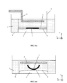
- Figure 1 and Figure 2 show schematic drawings illustrating a system according to an embodiment of the present invention, wherein a curled sample 1 comprising a thin silicon layer and at least one metal layer can be etched, i.e. wherein the at least one metal layer can be removed from the sample.
- Figures 1(a) and 2(a) show a cross section of the system along the y-direction, the y-direction being a direction in which the sample is not bent or curled.
- Figures 1(b) and 2(b) show a cross section of the system along the x-direction, the x-direction being a direction in which the sample is bent or curled and being substantially orthogonal to the y-direction.
- An electrochemical etching solution 2 such as e.g.
- a salt/acid aqueous solution also called electrolyte
- a container 8 e.g. a beaker made of a material or coated with a material that is not damaged by the electrochemical etching solution, such as for example glass or plastic.
- a platform 3 is provided at the bottom of the container 8 .
- This platform 3 can for example have a square shape in a plane parallel to the container bottom and it can for example be bent in one direction. In the embodiment illustrated in Figure 1 and Figure 2 , the platform 3 is bent along the x-direction and not along the y-direction. However, other shapes of the platform 3 can be used.
- the platform 3 is used to reverse the bending direction of a grid 4, carrying the sample 1 to be etched. This leads to good fixing of the sample between the grid 4 and a fixing element, e.g wire 5, and thus to good electrical contact to the clamped sample 1. Therefore, the shape of the platform 3 may be compatible with the shape of the grid 4.
- a flexible carrying element 4 a grid
- a frame 10 of smaller dimensions can be clamped in a frame 10 of smaller dimensions than the carrying element 4 such that the carrying element 4 can be in two different stable positions, each stable position corresponding to a different bending direction of the carrying element.
- the carrying element 4 can be bent in a first direction, e.g. as illustrated for example in Figure 5(b) , when introducing the sample 1 in the electrochemical processing solution or when removing the sample from the electrochemical processing solution.
- the carrying element 4 can be bent in a second, different, direction during electrochemical processing, as illustrated for example in Figure 5(a) .
- Figure 1 shows a system according to an embodiment of the present invention during introduction of the sample 1 into the container 8 comprising the etching solution 2.
- Figure 1(a) shows a cross-section along the y-direction;
- Figure 1(b) shows a cross-section along the x-direction.
- the sample is introduced in such a way that the direction in which it is bent is aligned with the direction in which the platform 3 is bent (in the example illustrated the x-direction).
- the sample 1 in the example shown a cylindrically curled sample 1 is placed on a holder comprising an electrically conductive bendable carrying element, grid 4, e.g. an electrically conductive grid such as a metallic grid 4. Other electrically conductive materials may be used for forming the grid 4.
- the curvature of the cylindrical sample has a smaller diameter than the curvature of the carrying element 4.
- a grid 4 is advantageous as it may improve liquid flows and release of bubbles.
- the sample 1 is kept in place on the grid 4 by means of a fixing element 5, for example a linear fixing element e.g. a wire 5.
- a fixing element for example a linear fixing element e.g. a wire 5.
- other fixing elements can be used, such as for example a rod or two small fixing elements, one at or close to two opposite extremities of the sample.
- the fixing element can be a rigid element or a flexible element or can be made of a material that allows some degree of deformation (such as e.g. rubber or foam).
- the fixing element can be attached to the grid or it can be a separate element.
- the sample 1 is bent in one direction and the wire 5 is oriented in a direction that is substantially equal to a direction in which the sample 1 is not bent.
- a handler 7 can be attached to the holder, to enable easy handling of the holder comprising the carrying element 4 and the fixing element 5.
- Figure 2 shows the system during electrochemical etching.
- Figure 2(a) shows a cross-section along the y-direction;
- Figure 2(b) shows a cross-section along the x-direction.
- the carrying element 4, e.g. bendable grid 4 is pushed to the platform 3 at the bottom of the container 8, such that it follows the shape of the platform 3.
- the grid 4 is electrically conductive and provides an electrical contact to the sample 1 to enable electrochemical processing.
- electrochemical processing e.g. etching
- the conductive carrying element, grid 4, and the wire 5 are pushed towards one another, thereby clamping the sample 1 and ensuring good electrical contact to the sample.
- an electrode e.g. negative electrode 6, is provided in the etching solution 2 in the etching solution 2 etching solution 2 a electrode, e.g. negative electrode 6, is provided in the etching solution 2 .
- the negative electrode 6 can for example be in the form of a plate or a grid and is made of an electrically conductive material, such as for example stainless steel or any other electrically conductive material that is resistant to the electrochemical process.
- an electrically conductive material such as for example stainless steel or any other electrically conductive material that is resistant to the electrochemical process.
- Figure 3 shows the system with the holder and the sample after electrochemical etching.
- a cross section along the x-direction is shown, i.e. along the direction in which the sample was initially bent.
- the sample is substantially uncurled. It can be removed from the etching bath by means of the holder comprising the carrying element 4 and the handler 7.
- the etched sample can be fragile, for example it can be a thin silicon layer (e.g. a few tens of micrometers thick).
- FIG. 1 to 3 a horizontal implementation of a system according to embodiments of the present invention is shown, other implementations are possible.
- a vertical implementation can be used allowing these compounds to fall on the bottom of the beaker e.g. by gravity.
- a platform 3 would not be provided at the bottom of the container 8 but it could be clamped to the grid holder, as illustrated in Figure 4 .
Landscapes
- Chemical & Material Sciences (AREA)
- Engineering & Computer Science (AREA)
- Chemical Kinetics & Catalysis (AREA)
- Electrochemistry (AREA)
- Materials Engineering (AREA)
- Metallurgy (AREA)
- Organic Chemistry (AREA)
- Sampling And Sample Adjustment (AREA)
Claims (11)
- System zum elektrochemischen Verarbeiten unebener Proben (1) und/oder Proben, welche während des elektrochemischen Verarbeitens ihre Form verändern können, umfassend einen Probenhalter zum Bereitstellen eines elektrischen Kontakts zu der Probe (1) während des elektrochemischen Verarbeitens,
wobei der Probenhalter ein gitterförmiges Trägerelement (4) und ein Befestigungselement (5) zum Einklemmen der Probe (1) zwischen dem Befestigungselement (5) und dem Trägerelement (4) umfasst, wobei folglich ein elektrischer Kontakt zu der Probe (1) bereitgestellt wird, während der Probe (1) ermöglicht wird, ihre Form zu verändern, ohne den elektrischen Kontakt zu unterbrechen. - System nach Anspruch 1, wobei das Trägerelement (4) in mindestens eine erste Richtung (x) gebogen ist.
- System nach einem der vorhergehenden Ansprüche, wobei das Trägerelement (4) ein flexibles Trägerelement ist, welches in einem Rahmen (10) von kleineren Abmessungen als den Abmessungen des Trägerelements (4) derartig eingeklemmt ist, dass das Trägerelement (4) eine von zwei stabilen Positionen einnehmen kann, wobei jede stabile Position einer verschiedenen Biegerichtung des Trägerelements (4) entspricht.
- System nach einem der Ansprüche 2 oder 3, welches weiterhin eine vorgeformte Plattform (3) zum Umkehren der Biegung des Trägerelements (4) beim Betrieb umfasst.
- System nach einem der vorhergehenden Ansprüche, wobei das Befestigungselement (5) ein lineares Befestigungselement ist.
- System nach einem der Ansprüche 1 bis 4, wobei das Befestigungselement (5) derartig ist, dass es beim Betrieb eine Kontaktfläche zwischen dem Befestigungselement (5) und einer Probe in der Form eines Punkts oder einer Fläche mit beschränkten Abmessungen von weniger als 10 % der entsprechenden Abmessungen der Probe bereitstellt.
- System nach Anspruch 6, wobei das Befestigungselement (5) derartig ist, dass die Kontaktfläche zwischen dem Befestigungselement (5) und einer Probe (1) beim Betrieb eine im Wesentlichen kreisförmige Kontaktfläche ist.
- System nach einem der vorhergehenden Ansprüche, wobei das Befestigungselement (5) und/oder das Trägerelement (4) elektrisch leitfähig ist.
- System nach einem der vorhergehenden Ansprüche, weiterhin eine Handhabevorrichtung (7) zum Handhaben des Probenhalters umfassend.
- Verfahren zum elektrochemischen Verarbeiten von unebenen Proben (1) und/oder von Proben, welche ihre Form während des Verarbeitens verändern können, Folgendes umfassend
Einklemmen einer Probe (1) zwischen einem gitterförmigen Trägerelement (4) und einem Befestigungselement (5) an mindestens einem Punkt, wobei folglich ein elektrischer Kontakt zu der Probe (1) bereitgestellt wird, und
elektrochemisches Verarbeiten der eingeklemmten Probe, während der elektrochemisch verarbeiteten Probe ermöglicht wird, ihre Form zu verändern, ohne den elektrischen Kontakt zu unterbrechen. - Verfahren nach Anspruch 10, wobei das Ermöglichen der elektrochemisch verarbeiteten Probe, ihre Form zu verändern, ein Umkehren der Biegerichtung des Trägerelements (4) umfasst, welches die Probe (1) trägt.
Applications Claiming Priority (2)
| Application Number | Priority Date | Filing Date | Title |
|---|---|---|---|
| US23899309P | 2009-09-01 | 2009-09-01 | |
| PCT/EP2010/060965 WO2011026696A1 (en) | 2009-09-01 | 2010-07-28 | Method for electrochemical processing of non-flat samples |
Publications (2)
| Publication Number | Publication Date |
|---|---|
| EP2473654A1 EP2473654A1 (de) | 2012-07-11 |
| EP2473654B1 true EP2473654B1 (de) | 2013-10-30 |
Family
ID=42945976
Family Applications (1)
| Application Number | Title | Priority Date | Filing Date |
|---|---|---|---|
| EP10737059.5A Not-in-force EP2473654B1 (de) | 2009-09-01 | 2010-07-28 | Verfahren zur elektrochemischen verarbeitung von unebenen proben |
Country Status (3)
| Country | Link |
|---|---|
| US (1) | US20120255869A1 (de) |
| EP (1) | EP2473654B1 (de) |
| WO (1) | WO2011026696A1 (de) |
Family Cites Families (6)
| Publication number | Priority date | Publication date | Assignee | Title |
|---|---|---|---|---|
| US5904820A (en) * | 1996-05-30 | 1999-05-18 | Brown; Howard | Holding clamp for electroplating articles |
| DE10019720A1 (de) * | 2000-04-20 | 2001-10-31 | Atotech Deutschland Gmbh | Verfahren und Vorrichtung zum elektrischen Kontaktieren von plattenförmigem Behandlungsgut bei elektrolytischen Prozessen |
| US7090750B2 (en) * | 2002-08-26 | 2006-08-15 | Micron Technology, Inc. | Plating |
| EP1863100A1 (de) | 2006-05-30 | 2007-12-05 | INTERUNIVERSITAIR MICROELEKTRONICA CENTRUM vzw (IMEC) | Verfahren zur Herstellung von dünnen Substraten |
| DE102006033353B4 (de) * | 2006-07-19 | 2010-11-18 | Höllmüller Maschinenbau GmbH | Verfahren und Vorrichtung zum Behandeln von flachen, zerbrechlichen Substraten |
| DE202006012842U1 (de) * | 2006-08-18 | 2007-01-11 | Wolf-Thilo Fortak Industrieberatung und techn. Service für die Galvanotechnik | Vorrichtung zum Anodisieren von Behandlungsgut |
-
2010
- 2010-07-28 WO PCT/EP2010/060965 patent/WO2011026696A1/en not_active Ceased
- 2010-07-28 EP EP10737059.5A patent/EP2473654B1/de not_active Not-in-force
-
2012
- 2012-02-29 US US13/408,899 patent/US20120255869A1/en not_active Abandoned
Also Published As
| Publication number | Publication date |
|---|---|
| US20120255869A1 (en) | 2012-10-11 |
| EP2473654A1 (de) | 2012-07-11 |
| WO2011026696A1 (en) | 2011-03-10 |
Similar Documents
| Publication | Publication Date | Title |
|---|---|---|
| US10751986B2 (en) | Systems for transferring graphene | |
| US6448155B1 (en) | Production method of semiconductor base material and production method of solar cell | |
| JPH11195775A (ja) | 半導体基板および薄膜半導体素子およびそれらの製造方法ならびに陽極化成装置 | |
| CN101680106B (zh) | 硅基材的加工方法、其加工品和加工装置 | |
| EP1385199A1 (de) | Verfahren zur Herstellung von Dünnfilmelementen für Solarzellen oder SOI Anwendungen | |
| CN105377755A (zh) | 转移石墨烯的电化学方法 | |
| CN105073412B (zh) | 薄玻璃长条体 | |
| KR101317133B1 (ko) | 태양전지용 전기 도금을 위한 기판 캐리어 장치 | |
| TW201514110A (zh) | 膜狀玻璃的製造方法、電子元件的製造方法及玻璃膜積層體的製造方法 | |
| WO2014200827A1 (en) | Methods and apparatuses for delaminating process pieces | |
| US10037896B2 (en) | Electro-assisted transfer and fabrication of wire arrays | |
| US9522521B2 (en) | Apparatus and method for separating a stacked arrangement | |
| CN104603930B (zh) | 分离层的方法 | |
| US20120255869A1 (en) | System and method for electrochemical processing of non-flat samples | |
| US20090280588A1 (en) | Method of forming an electronic device including removing a differential etch layer | |
| WO2017074867A1 (en) | Transfer of vertically aligned ultra-high density nanowires onto flexible substrates | |
| US20170167044A1 (en) | Systems, methods and apparatus for electroplating photovoltaic cells | |
| CN201397821Y (zh) | 石墨载板 | |
| CN111180392A (zh) | 基于绝缘体上硅大批量获得大尺寸单晶硅纳米膜的方法 | |
| JP2004087981A (ja) | エッチング装置およびエッチング方法 | |
| KR101645533B1 (ko) | 기판 식각 방법 및 장치, 기판 식각용 스탬프 및 이의 제조 방법 | |
| KR20180036262A (ko) | 그래핀 도핑 방법 및 제조 방법과, 이에 의해 제조되는 그래핀 | |
| CN119650424A (zh) | 一种半导体薄膜及其制备方法与应用 | |
| EP1385200B1 (de) | Verfahren zur Herstellung von Dünnschichtbauelementen für Solarzellen oder SOI-Anwendungen | |
| CN222600958U (zh) | 一种清洗腐蚀夹具 |
Legal Events
| Date | Code | Title | Description |
|---|---|---|---|
| PUAI | Public reference made under article 153(3) epc to a published international application that has entered the european phase |
Free format text: ORIGINAL CODE: 0009012 |
|
| 17P | Request for examination filed |
Effective date: 20120327 |
|
| AK | Designated contracting states |
Kind code of ref document: A1 Designated state(s): AL AT BE BG CH CY CZ DE DK EE ES FI FR GB GR HR HU IE IS IT LI LT LU LV MC MK MT NL NO PL PT RO SE SI SK SM TR |
|
| DAX | Request for extension of the european patent (deleted) | ||
| GRAP | Despatch of communication of intention to grant a patent |
Free format text: ORIGINAL CODE: EPIDOSNIGR1 |
|
| GRAS | Grant fee paid |
Free format text: ORIGINAL CODE: EPIDOSNIGR3 |
|
| GRAA | (expected) grant |
Free format text: ORIGINAL CODE: 0009210 |
|
| RAP1 | Party data changed (applicant data changed or rights of an application transferred) |
Owner name: KATHOLIEKE UNIVERSITEIT LEUVEN Owner name: IMEC |
|
| AK | Designated contracting states |
Kind code of ref document: B1 Designated state(s): AL AT BE BG CH CY CZ DE DK EE ES FI FR GB GR HR HU IE IS IT LI LT LU LV MC MK MT NL NO PL PT RO SE SI SK SM TR |
|
| REG | Reference to a national code |
Ref country code: GB Ref legal event code: FG4D |
|
| REG | Reference to a national code |
Ref country code: CH Ref legal event code: EP |
|
| REG | Reference to a national code |
Ref country code: AT Ref legal event code: REF Ref document number: 638521 Country of ref document: AT Kind code of ref document: T Effective date: 20131115 |
|
| REG | Reference to a national code |
Ref country code: IE Ref legal event code: FG4D |
|
| REG | Reference to a national code |
Ref country code: DE Ref legal event code: R096 Ref document number: 602010011347 Country of ref document: DE Effective date: 20131224 |
|
| REG | Reference to a national code |
Ref country code: NL Ref legal event code: VDEP Effective date: 20131030 |
|
| REG | Reference to a national code |
Ref country code: AT Ref legal event code: MK05 Ref document number: 638521 Country of ref document: AT Kind code of ref document: T Effective date: 20131030 |
|
| REG | Reference to a national code |
Ref country code: LT Ref legal event code: MG4D |
|
| PG25 | Lapsed in a contracting state [announced via postgrant information from national office to epo] |
Ref country code: NO Free format text: LAPSE BECAUSE OF FAILURE TO SUBMIT A TRANSLATION OF THE DESCRIPTION OR TO PAY THE FEE WITHIN THE PRESCRIBED TIME-LIMIT Effective date: 20140130 Ref country code: BE Free format text: LAPSE BECAUSE OF FAILURE TO SUBMIT A TRANSLATION OF THE DESCRIPTION OR TO PAY THE FEE WITHIN THE PRESCRIBED TIME-LIMIT Effective date: 20131030 Ref country code: NL Free format text: LAPSE BECAUSE OF FAILURE TO SUBMIT A TRANSLATION OF THE DESCRIPTION OR TO PAY THE FEE WITHIN THE PRESCRIBED TIME-LIMIT Effective date: 20131030 Ref country code: FI Free format text: LAPSE BECAUSE OF FAILURE TO SUBMIT A TRANSLATION OF THE DESCRIPTION OR TO PAY THE FEE WITHIN THE PRESCRIBED TIME-LIMIT Effective date: 20131030 Ref country code: SE Free format text: LAPSE BECAUSE OF FAILURE TO SUBMIT A TRANSLATION OF THE DESCRIPTION OR TO PAY THE FEE WITHIN THE PRESCRIBED TIME-LIMIT Effective date: 20131030 Ref country code: IS Free format text: LAPSE BECAUSE OF FAILURE TO SUBMIT A TRANSLATION OF THE DESCRIPTION OR TO PAY THE FEE WITHIN THE PRESCRIBED TIME-LIMIT Effective date: 20140228 Ref country code: LT Free format text: LAPSE BECAUSE OF FAILURE TO SUBMIT A TRANSLATION OF THE DESCRIPTION OR TO PAY THE FEE WITHIN THE PRESCRIBED TIME-LIMIT Effective date: 20131030 Ref country code: HR Free format text: LAPSE BECAUSE OF FAILURE TO SUBMIT A TRANSLATION OF THE DESCRIPTION OR TO PAY THE FEE WITHIN THE PRESCRIBED TIME-LIMIT Effective date: 20131030 |
|
| PG25 | Lapsed in a contracting state [announced via postgrant information from national office to epo] |
Ref country code: ES Free format text: LAPSE BECAUSE OF FAILURE TO SUBMIT A TRANSLATION OF THE DESCRIPTION OR TO PAY THE FEE WITHIN THE PRESCRIBED TIME-LIMIT Effective date: 20131030 Ref country code: AT Free format text: LAPSE BECAUSE OF FAILURE TO SUBMIT A TRANSLATION OF THE DESCRIPTION OR TO PAY THE FEE WITHIN THE PRESCRIBED TIME-LIMIT Effective date: 20131030 Ref country code: LV Free format text: LAPSE BECAUSE OF FAILURE TO SUBMIT A TRANSLATION OF THE DESCRIPTION OR TO PAY THE FEE WITHIN THE PRESCRIBED TIME-LIMIT Effective date: 20131030 Ref country code: CY Free format text: LAPSE BECAUSE OF FAILURE TO SUBMIT A TRANSLATION OF THE DESCRIPTION OR TO PAY THE FEE WITHIN THE PRESCRIBED TIME-LIMIT Effective date: 20131030 |
|
| PG25 | Lapsed in a contracting state [announced via postgrant information from national office to epo] |
Ref country code: PT Free format text: LAPSE BECAUSE OF FAILURE TO SUBMIT A TRANSLATION OF THE DESCRIPTION OR TO PAY THE FEE WITHIN THE PRESCRIBED TIME-LIMIT Effective date: 20140228 |
|
| PG25 | Lapsed in a contracting state [announced via postgrant information from national office to epo] |
Ref country code: EE Free format text: LAPSE BECAUSE OF FAILURE TO SUBMIT A TRANSLATION OF THE DESCRIPTION OR TO PAY THE FEE WITHIN THE PRESCRIBED TIME-LIMIT Effective date: 20131030 |
|
| REG | Reference to a national code |
Ref country code: DE Ref legal event code: R097 Ref document number: 602010011347 Country of ref document: DE |
|
| PG25 | Lapsed in a contracting state [announced via postgrant information from national office to epo] |
Ref country code: PL Free format text: LAPSE BECAUSE OF FAILURE TO SUBMIT A TRANSLATION OF THE DESCRIPTION OR TO PAY THE FEE WITHIN THE PRESCRIBED TIME-LIMIT Effective date: 20131030 Ref country code: SK Free format text: LAPSE BECAUSE OF FAILURE TO SUBMIT A TRANSLATION OF THE DESCRIPTION OR TO PAY THE FEE WITHIN THE PRESCRIBED TIME-LIMIT Effective date: 20131030 Ref country code: CZ Free format text: LAPSE BECAUSE OF FAILURE TO SUBMIT A TRANSLATION OF THE DESCRIPTION OR TO PAY THE FEE WITHIN THE PRESCRIBED TIME-LIMIT Effective date: 20131030 Ref country code: RO Free format text: LAPSE BECAUSE OF FAILURE TO SUBMIT A TRANSLATION OF THE DESCRIPTION OR TO PAY THE FEE WITHIN THE PRESCRIBED TIME-LIMIT Effective date: 20131030 Ref country code: IT Free format text: LAPSE BECAUSE OF FAILURE TO SUBMIT A TRANSLATION OF THE DESCRIPTION OR TO PAY THE FEE WITHIN THE PRESCRIBED TIME-LIMIT Effective date: 20131030 |
|
| PLBE | No opposition filed within time limit |
Free format text: ORIGINAL CODE: 0009261 |
|
| STAA | Information on the status of an ep patent application or granted ep patent |
Free format text: STATUS: NO OPPOSITION FILED WITHIN TIME LIMIT |
|
| PG25 | Lapsed in a contracting state [announced via postgrant information from national office to epo] |
Ref country code: DK Free format text: LAPSE BECAUSE OF FAILURE TO SUBMIT A TRANSLATION OF THE DESCRIPTION OR TO PAY THE FEE WITHIN THE PRESCRIBED TIME-LIMIT Effective date: 20131030 |
|
| 26N | No opposition filed |
Effective date: 20140731 |
|
| REG | Reference to a national code |
Ref country code: DE Ref legal event code: R097 Ref document number: 602010011347 Country of ref document: DE Effective date: 20140731 |
|
| REG | Reference to a national code |
Ref country code: DE Ref legal event code: R119 Ref document number: 602010011347 Country of ref document: DE |
|
| PG25 | Lapsed in a contracting state [announced via postgrant information from national office to epo] |
Ref country code: SI Free format text: LAPSE BECAUSE OF FAILURE TO SUBMIT A TRANSLATION OF THE DESCRIPTION OR TO PAY THE FEE WITHIN THE PRESCRIBED TIME-LIMIT Effective date: 20131030 Ref country code: LU Free format text: LAPSE BECAUSE OF FAILURE TO SUBMIT A TRANSLATION OF THE DESCRIPTION OR TO PAY THE FEE WITHIN THE PRESCRIBED TIME-LIMIT Effective date: 20140728 |
|
| REG | Reference to a national code |
Ref country code: CH Ref legal event code: PL |
|
| GBPC | Gb: european patent ceased through non-payment of renewal fee |
Effective date: 20140728 |
|
| REG | Reference to a national code |
Ref country code: IE Ref legal event code: MM4A |
|
| REG | Reference to a national code |
Ref country code: DE Ref legal event code: R119 Ref document number: 602010011347 Country of ref document: DE Effective date: 20150203 |
|
| REG | Reference to a national code |
Ref country code: FR Ref legal event code: ST Effective date: 20150331 |
|
| PG25 | Lapsed in a contracting state [announced via postgrant information from national office to epo] |
Ref country code: LI Free format text: LAPSE BECAUSE OF NON-PAYMENT OF DUE FEES Effective date: 20140731 Ref country code: DE Free format text: LAPSE BECAUSE OF NON-PAYMENT OF DUE FEES Effective date: 20150203 Ref country code: CH Free format text: LAPSE BECAUSE OF NON-PAYMENT OF DUE FEES Effective date: 20140731 |
|
| PG25 | Lapsed in a contracting state [announced via postgrant information from national office to epo] |
Ref country code: FR Free format text: LAPSE BECAUSE OF NON-PAYMENT OF DUE FEES Effective date: 20140731 Ref country code: GB Free format text: LAPSE BECAUSE OF NON-PAYMENT OF DUE FEES Effective date: 20140728 |
|
| PG25 | Lapsed in a contracting state [announced via postgrant information from national office to epo] |
Ref country code: IE Free format text: LAPSE BECAUSE OF NON-PAYMENT OF DUE FEES Effective date: 20140728 |
|
| PG25 | Lapsed in a contracting state [announced via postgrant information from national office to epo] |
Ref country code: SM Free format text: LAPSE BECAUSE OF FAILURE TO SUBMIT A TRANSLATION OF THE DESCRIPTION OR TO PAY THE FEE WITHIN THE PRESCRIBED TIME-LIMIT Effective date: 20131030 Ref country code: MC Free format text: LAPSE BECAUSE OF FAILURE TO SUBMIT A TRANSLATION OF THE DESCRIPTION OR TO PAY THE FEE WITHIN THE PRESCRIBED TIME-LIMIT Effective date: 20131030 |
|
| PG25 | Lapsed in a contracting state [announced via postgrant information from national office to epo] |
Ref country code: BG Free format text: LAPSE BECAUSE OF FAILURE TO SUBMIT A TRANSLATION OF THE DESCRIPTION OR TO PAY THE FEE WITHIN THE PRESCRIBED TIME-LIMIT Effective date: 20131030 Ref country code: MT Free format text: LAPSE BECAUSE OF FAILURE TO SUBMIT A TRANSLATION OF THE DESCRIPTION OR TO PAY THE FEE WITHIN THE PRESCRIBED TIME-LIMIT Effective date: 20131030 Ref country code: GR Free format text: LAPSE BECAUSE OF FAILURE TO SUBMIT A TRANSLATION OF THE DESCRIPTION OR TO PAY THE FEE WITHIN THE PRESCRIBED TIME-LIMIT Effective date: 20140131 |
|
| PG25 | Lapsed in a contracting state [announced via postgrant information from national office to epo] |
Ref country code: TR Free format text: LAPSE BECAUSE OF FAILURE TO SUBMIT A TRANSLATION OF THE DESCRIPTION OR TO PAY THE FEE WITHIN THE PRESCRIBED TIME-LIMIT Effective date: 20131030 Ref country code: HU Free format text: LAPSE BECAUSE OF FAILURE TO SUBMIT A TRANSLATION OF THE DESCRIPTION OR TO PAY THE FEE WITHIN THE PRESCRIBED TIME-LIMIT; INVALID AB INITIO Effective date: 20100728 |
|
| PG25 | Lapsed in a contracting state [announced via postgrant information from national office to epo] |
Ref country code: MK Free format text: LAPSE BECAUSE OF FAILURE TO SUBMIT A TRANSLATION OF THE DESCRIPTION OR TO PAY THE FEE WITHIN THE PRESCRIBED TIME-LIMIT Effective date: 20131030 |
|
| PG25 | Lapsed in a contracting state [announced via postgrant information from national office to epo] |
Ref country code: AL Free format text: LAPSE BECAUSE OF FAILURE TO SUBMIT A TRANSLATION OF THE DESCRIPTION OR TO PAY THE FEE WITHIN THE PRESCRIBED TIME-LIMIT Effective date: 20131030 |