EP2474095B1 - Commutateur inductif retroeclaire - Google Patents
Commutateur inductif retroeclaire Download PDFInfo
- Publication number
- EP2474095B1 EP2474095B1 EP10745503.2A EP10745503A EP2474095B1 EP 2474095 B1 EP2474095 B1 EP 2474095B1 EP 10745503 A EP10745503 A EP 10745503A EP 2474095 B1 EP2474095 B1 EP 2474095B1
- Authority
- EP
- European Patent Office
- Prior art keywords
- layer
- inductive
- substrate
- sense coil
- light
- Prior art date
- Legal status (The legal status is an assumption and is not a legal conclusion. Google has not performed a legal analysis and makes no representation as to the accuracy of the status listed.)
- Active
Links
Images

Classifications
-
- H—ELECTRICITY
- H03—ELECTRONIC CIRCUITRY
- H03K—PULSE TECHNIQUE
- H03K17/00—Electronic switching or gating, i.e. not by contact-making and –breaking
- H03K17/94—Electronic switching or gating, i.e. not by contact-making and –breaking characterised by the way in which the control signals are generated
- H03K17/945—Proximity switches
- H03K17/95—Proximity switches using a magnetic detector
- H03K17/952—Proximity switches using a magnetic detector using inductive coils
-
- H—ELECTRICITY
- H03—ELECTRONIC CIRCUITRY
- H03K—PULSE TECHNIQUE
- H03K17/00—Electronic switching or gating, i.e. not by contact-making and –breaking
- H03K17/94—Electronic switching or gating, i.e. not by contact-making and –breaking characterised by the way in which the control signals are generated
- H03K17/96—Touch switches
-
- H—ELECTRICITY
- H03—ELECTRONIC CIRCUITRY
- H03K—PULSE TECHNIQUE
- H03K17/00—Electronic switching or gating, i.e. not by contact-making and –breaking
- H03K17/94—Electronic switching or gating, i.e. not by contact-making and –breaking characterised by the way in which the control signals are generated
- H03K17/96—Touch switches
- H03K17/962—Capacitive touch switches
-
- H—ELECTRICITY
- H03—ELECTRONIC CIRCUITRY
- H03K—PULSE TECHNIQUE
- H03K2217/00—Indexing scheme related to electronic switching or gating, i.e. not by contact-making or -breaking covered by H03K17/00
- H03K2217/94—Indexing scheme related to electronic switching or gating, i.e. not by contact-making or -breaking covered by H03K17/00 characterised by the way in which the control signal is generated
- H03K2217/96—Touch switches
- H03K2217/96038—Inductive touch switches
-
- H—ELECTRICITY
- H03—ELECTRONIC CIRCUITRY
- H03K—PULSE TECHNIQUE
- H03K2217/00—Indexing scheme related to electronic switching or gating, i.e. not by contact-making or -breaking covered by H03K17/00
- H03K2217/94—Indexing scheme related to electronic switching or gating, i.e. not by contact-making or -breaking covered by H03K17/00 characterised by the way in which the control signal is generated
- H03K2217/96—Touch switches
- H03K2217/96042—Touch switches with illumination
-
- H—ELECTRICITY
- H03—ELECTRONIC CIRCUITRY
- H03K—PULSE TECHNIQUE
- H03K2217/00—Indexing scheme related to electronic switching or gating, i.e. not by contact-making or -breaking covered by H03K17/00
- H03K2217/94—Indexing scheme related to electronic switching or gating, i.e. not by contact-making or -breaking covered by H03K17/00 characterised by the way in which the control signal is generated
- H03K2217/96—Touch switches
- H03K2217/96042—Touch switches with illumination
- H03K2217/96046—Key-pad combined with display, back-lit
-
- H—ELECTRICITY
- H03—ELECTRONIC CIRCUITRY
- H03K—PULSE TECHNIQUE
- H03K2217/00—Indexing scheme related to electronic switching or gating, i.e. not by contact-making or -breaking covered by H03K17/00
- H03K2217/94—Indexing scheme related to electronic switching or gating, i.e. not by contact-making or -breaking covered by H03K17/00 characterised by the way in which the control signal is generated
- H03K2217/965—Switches controlled by moving an element forming part of the switch
- H03K2217/9653—Switches controlled by moving an element forming part of the switch with illumination
- H03K2217/9655—Switches controlled by moving an element forming part of the switch with illumination using a single or more light guides
Definitions
- the present disclosure relates to inductive touch sensor keys or buttons, and, more particularly, to backlighting of the inductive touch sensor keys or buttons.
- Each inductive touch sensor key or button comprises an inductive sensor on a substrate, a thin non-magnetic spacer layer over the inductive touch sensor, and a deformable metal target layer (e.g., key or button) over the thin non-magnetic spacer layer.
- a deformable metal target layer e.g., key or button
- the inductive sensor detects a change in its impedance. This change in impedance is detected and is used to indicate that the key or button has been pressed.
- the deformable metal target layer is light opaque and therefore precludes backlighting thereof.
- Existing published solutions for inductive touch sensor designs are mechanically very thin. They rely on simple flat spacer layers less than .020 inch thick and continuous conductive metal sheets for targets that do not allow light to pass therethrough.
- WO 2008/012491 A1 relates to an inductive sensor keys panel to measure the deformation of a body.
- WO2006/064234 A1 discloses an inductive button detector, whereby measurement of the ratio of two inductances indicates a position of a first body relative to a second body.
- a molded spacer layer and a discrete metal disk may be used for the inductive target.
- inductive touch sensor keys may be backlit.
- Backlighting of inductive touch sensor keys or buttons is especially desirable for use in appliances, automotive controls, consumer products such as television set top box converters for cable or satellite television reception, security entry pads, intercom buttons, computers, industrial control panels, etc.
- Backlighting of the keys or buttons may be used to indicate that the key or button has been pressed, e.g ., visual feedback, and/or improved visibility under poor lighting conditions.
- Inductive touch buttons in most cases require that the metal fascia be the target, but according to the teachings of this disclosure it would be moved away from the inductive coil to the point where it will not work as the target. To counteract this, a suspended target proximate to the inductive sensor coil is used. By configuring the lighted inductive touch buttons as such, height may be added to the inductive touch panel design that will allow placement of light emitting diodes (LEDs) on the top and/or bottom side(s) of the circuit board comprising the inductive sensor coil.
- LEDs light emitting diodes
- a molded plastic layer(s) may be used to create light pipes that allow for backlighting of the inductive touch sensor buttons.
- a metallic target layer is attached and/or molded on the plastic layer proximate to the inductive sensor coil. As this metallic target layer moves closer to the inductor sensor coil when the button is depressed, the impedance of the inductor sensor coil thereby changes and is detected.
- the metallic target layer may also be used as a shield to prevent or reduce hot (bright) spots in the lighting of the inductive touch sensor button.
- the material that holds the suspended metallic target may be translucent and function as a light pipe for the light from a light source, e.g., light emitting diodes (LEDs). This translucent material may also function as a seal for the holes that may now be placed in the metal cover to allow light to pass therethrough.
- the material that is used as the spacer surrounding the inductive coil may be of a non-translucent material so as to prevent bleeding of light from one adjacent button to the next.
- the light source LEDs do not have to be mounted on the top side of the circuit board, as they can be mounted elsewhere as needed. Also the top layer does not have to be flat or even metal, and it may be curved or use an over-mold process for sealing of the button.
- a backlit inductive touch sensor key according to claim 1 is disclosed.
- a backlit inductive touch sensor key according to claim 2 is disclosed.
- a backlit inductive touch sensor key according to claim 3 is disclosed.
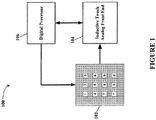
- a digital processor 106 e.g., a microprocessor, microcomputer, digital signal processor (DSP), application specific integrated circuit (ASIC), programmable logic array (PLA), etc.
- DSP digital signal processor
- ASIC application specific integrated circuit
- PPA programmable logic array
- AFE inductive touch analog front end
- Typical inductive touch sensor keys 102 may comprise Microchip inductive mTouchTM sensors more fully described at www.microchip.com .
- the digital processor 106 and AFE 104 may be part of a mixed signal (analog and digital circuits) integrated circuit device.
- the inductive touch AFE 104 facilitates, with a single low-cost integrated circuit device, all active functions used in determining when there is actuation of inductive sensors, e.g., by pressing and deflecting a target key that changes the impedance value of an associated inductive sensor.
- the inductive touch AFE 104 measures the impedance value of each sensor of the matrix of inductive touch sensor keys 102 and converts the impedance values into respective analog direct current (dc) voltages that are read and converted into digital values by the digital processor 106.
- dc direct current
- the digital processor 106 supplies clock and control functions to the inductive touch AFE 104, reads the analog voltage detector output of the inductive touch AFE 104, and selects each key of the matrix of inductive touch sensor keys 102. When actuation of a key of the matrix of inductive touch sensor keys 102 is determined, the digital processor 106 will take an appropriate action.
- each key (touch buttons) of the matrix of inductive touch sensor keys 102 is illuminated, as more fully disclosed hereinafter.
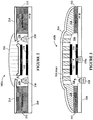
- FIG. 2 depicted is a schematic elevational view of a back-lighted inductive touch key comprising a light transmissive button in combination with an over-layer having holes therein for light to pass therethrough, according to a specific example embodiment of this disclosure.
- a back-lighted inductive touch key 102a comprises a substrate 210, e.g., printed circuit board (PCB); an inductive sense coil 220, a light source, e.g., light emitting diodes (LEDs) 218; a non-translucent (opaque) molded spacer layer 212 surrounds the inductive sense coil 220 and LEDs 218, an over-layer 214 having openings therein for light from the LEDs 218 to pass therethrough, and an over-mold button 216 that is translucent for illumination thereof by the light from the LEDs 218.
- a substrate 210 e.g., printed circuit board (PCB)
- an inductive sense coil 220 e.g., a light source, e.g., light emitting diodes (LEDs) 218
- a non-translucent (opaque) molded spacer layer 212 surrounds the inductive sense coil 220 and LEDs 218, an over-layer 214 having openings therein for light from
- a metallic target 222 is disposed on a surface of the over-layer 214 proximate to the inductive sense coil 220.
- a metallic over-layer 214 may be for example, but is not limited to, aluminum, steel, stainless steel, copper, titanium, etc.
- a non-metallic over-layer 214 may be for example, but is not limited to, plastic, Teflon, polyamide, etc.
- the molded spacer layer 212 surrounding the inductive sense coil 220 and LEDs 218 is substantially non-translucent (opaque) so that light does not bleed over to another adjacent back-lighted inductive touch key (not shown).
- the LEDs 218 (light source) may be mounted on top of the substrate 210, and inside of a cavity 226 formed by the substrate 210, the molded spacer layer 212 and the over-layer 214.
- the LEDs 218 may also be mounted in the substrate 210 or on the opposite side thereof (e.g., LED 318a or LED 318, respectively, of Figure 3 ). LEDs 218 may be on either side and/or inside of the inductive sense coil 220.
- the over-mold button 216 is flexible wherein when pushed (actuated) by an external force, e.g., push from a finger, the over-layer 214 portion over inductive sense coil 220 moves closer thereto and thereby changes the impedance thereof. If the over-layer 214 is non-metallic and does not affect the impedance of the inductive sense coil 220, then a metallic target 222 may be attached to the over-layer 214 proximate to the inductive sense coil 220.
- the inductive touch AFE 104 ( Figure 1 ) detects this change in impedance of the sense coil 220 and indicates this event to the digital processor 106 for appropriate action to be taken.
- a change in intensity and/or color of the light from the LEDs 218 may indicate successful actuation of this specific inductive touch sensor key 102a. It is contemplated and within the scope of this disclosure that the over-layer 214 portion over the inductive sense coil 220 and/or the target 222 may be any type of material that affects the impedance value of the inductive sense coil 220 when there is a change in distance therebetween.
- a back-lighted inductive touch key 102b comprises a substrate 310, e.g., a printed circuit board (PCB); an inductive sense coil 320, a light source, e.g., light emitting diodes (LEDs) 318 and/or 318a; a non-translucent (opaque) molded spacer layer 312 surrounds the inductive sense coil 320 and LEDs 318, a light transmissive layer 316, a metallic target 322 attached to the layer 316 and proximate to the inductive sense coil 320, and an over-layer 314 that a portion thereof is either light transmissive or has openings therein for light from the LEDs 318 to pass therethrough.
- a substrate 310 e.g., a printed circuit board (PCB)
- an inductive sense coil 320 e.g., a light source, e.g., light emitting diodes (LEDs) 318 and/or 318a
- the molded spacer layer 312 surrounding the inductive sense coil 320 and LEDs 318 and/or 318a is substantially non-translucent (opaque) so that light does not bleed over to another adjacent back-lighted inductive touch key (not shown).
- the LEDs 318 (light source) may be mounted on top of the substrate 310 ( e.g., LED 218 of Figure 2 ) and inside of a cavity 326 formed by the substrate 310, the molded spacer layer 312 and the light transmissive layer 316.
- the LEDs 318a may also be mounted in the substrate 310 or on the opposite side thereof, e.g., LED 318. LEDs 318 may be on either side and/or inside of the inductive sense coil 320.
- the light transmissive layer 316 may be flexible wherein when pushed (actuated) by an external force, e.g., push from a finger, the light transmissive layer 316 portion over inductive sense coil 320 moves closer thereto and thereby changes the impedance thereof. If the light transmissive layer 316 is not made of a flexible and/or light transmissive material then openings or gaps 324 may be disposed within a portion of the light transmissive layer 316 for light from the LEDs 318 to pass therethrough.
- the over-layer 314 may be used for protection from physical abuse and/or harmful water and/or chemical infiltration.
- the over-layer 314 may comprise a thin metal layer, e.g., aluminum, steel, stainless steel, copper, titanium, etc.. or a non-metallic layer, e.g., plastic, Teflon, polyamide, etc. If the material of the over-layer 314 is not light transmissive then opening may be placed therein (not shown) for light transmission therethrough.
- the light transmissive layer 316 is non-metallic and does not affect the impedance of the inductive sense coil 320, then a metallic target 322 may be attached to the light transmissive layer 316 proximate to the inductive sense coil 320.
- the inductive touch AFE 104 ( Figure 1 ) detects a change in impedance of the sense coil 320 and indicates this event to the digital processor 106 for appropriate action to be taken. For example, but not limited to, a change in intensity and/or color of the light from the LEDs 318 may indicate successful actuation of this specific inductive touch sensor key 102b.
- the light transmissive layer 316 and/or the target 322 over the inductive sense coil 320 may be any type of material that affects the impedance value of the inductive sense coil 320 when there is a change in distance therebetween.
- the target 322 may also provide light shielding an light diffusion from the light source, e.g ., LED 318a, so as to prevent light intensity "hot spots" in the back-lighted inductive touch key 102b.
- a back-lighted inductive touch key 102c comprises a substrate 410, e.g., a printed circuit board (PCB); an inductive sense coil 420, a light source, e.g., light emitting diodes (LEDs) 418; a non-translucent (opaque) molded spacer layer 412 surrounds the inductive sense coil 420 and LEDs 418, a light transmissive (translucent) layer 416, a metallic target 422 attached to the layer 416 and proximate to the inductive sense coil 420, and an over-layer fascia 414 that a portion thereof is either light transmissive or has openings therein for light from the light transmissive layer 416 to pass therethrough.
- a substrate 410 e.g., a printed circuit board (PCB)
- an inductive sense coil 420 e.g., a light source, e.g., light emitting diodes (LEDs) 418
- the over-layer fascia 414 may be substantially flat and attached to the non-translucent (opaque) molded spacer layer 412 for support thereof.
- the light transmissive layer 416 is attached to the over-layer fascia 414 and in cooperation therewith moves the metallic target 422 closer to the inductive sense coil 420 when a force is applied to the over-layer fascia 414 proximate to the light transmissive layer 416.
- the light transmissive layer 416 serves as a light pipe for illumination of an information area of the over-layer fascia 414.
- the material of the over-layer fascia 414 may comprise metal or be nonmetallic as desired, and if this material is opaque (non-light transmissive), openings 428 therein may be provided for light to pass therethrough.
- the molded spacer layer 412 surrounding the inductive sense coil 420 and LEDs 418 is substantially non-translucent (opaque) so that light does not bleed over to another adjacent back-lighted inductive touch key (not shown).
- the LEDs 418 (light source) may be mounted on top of the substrate 410 ( e.g., LED 218 of Figure 2 ) and inside of a cavity 426 formed by the substrate 410, the molded spacer layer 412 and the over-layer fascia 414.
- the LEDs 418 may also be mounted in the substrate 410, e.g., LED 318a. LEDs 418 may be on either side and/or inside of the inductive sense coil 420.
- the over-layer fascia 414 may be used for protection from physical abuse and/or harmful water and/or chemical infiltration.
- the over-layer fascia 414 may comprise a thin metal layer such as for example, but is not limited to, aluminum, steel, stainless steel, copper, titanium, etc., or a non-metallic layer such as for example, but is not limited to, plastic, Teflon, polyamide, etc.
- the inductive touch AFE 104 detects a change in impedance of the sense coil 420 and indicates this event to the digital processor 106 for appropriate action to be taken. For example, but not limited to, a change in intensity and/or color of the light from the LEDs 418 may indicate successful actuation of this specific inductive touch sensor key 102c. It is contemplated and within the scope of this disclosure that the light transmissive layer 416 and/or the target 422 over the inductive sense coil 420 may be any type of material that affects the impedance value of the inductive sense coil 420 when there is a change in distance therebetween.
Landscapes
- Push-Button Switches (AREA)
- Switch Cases, Indication, And Locking (AREA)
- Switches That Are Operated By Magnetic Or Electric Fields (AREA)
Claims (15)
- Touche de capteur tactile inductif rétroéclairé, comprenant :un substrat (210) ;une bobine de détection inductive (220) sur le substrat (210) ;une source de lumière (218 ; 318 ; 418) montée sur le dessus du substrat (210), dans le substrat (210) ou sur le côté opposé du substrat (210), dans laquelle la source de lumière (218 ; 318 ; 418) est montée d'un côté ou de l'autre ou à l'intérieur de la bobine de détection inductive (220) ;une couche d'espacement opaque (212) située sur le substrat (210) et présentant une ouverture qui entoure la bobine de détection inductive (220) et la source de lumière (218 ; 318 ; 418) ;une couche de protection (214) dotée d'ouvertures destinées à laisser passer la lumière provenant de la source de lumière, la couche de protection (214) étant montée sur la couche d'espacement (212) et formant une cavité comprenant une cavité de transmission de lumière (226) entre le substrat et la couche de protection ;un bouton surmoulé (216) fixé à un côté de la couche de protection (214) opposé à la cavité de transmission de lumière (226), le bouton surmoulé (216) transmettant la lumière ; etune cible métallique (222) fixée directement au-dessus de la bobine de détection inductive (220) dans la cavité de transmission de lumière (226) à une face de la couche de protection (214) qui peut être poussée dans la cavité vers la bobine de détection inductive (220), à la suite de quoi une valeur d'impédance de la bobine de détection inductive (220) change.
- Touche de capteur tactile inductif rétroéclairé, comprenant :un substrat (310) ;une bobine de détection inductive (320) sur le substrat (310) ;une source de lumière (318) montée sur le dessus du substrat (310), dans le substrat (310) ou sur le côté opposé du substrat (310), dans laquelle la source de lumière (318) est montée d'un côté ou de l'autre ou à l'intérieur de la bobine de détection inductive (320) ;une couche d'espacement opaque (312) montée sur le substrat (310) et présentant une ouverture qui entoure la bobine de détection inductive (320) et la source de lumière (318) ; etune couche flexible (316) d'un matériau transmettant la lumière, dans laquelle la couche flexible (316) s'étend sur la bobine de détection inductive (320) et la source de lumière (318), et est fixée à la couche d'espacement opaque (312), dans laquelle une cavité de transmission de lumière (326) est formée entre le substrat (310) et la couche flexible (316) ;une couche de protection (314) couvrant ladite couche flexible (316) transmettant la lumière ou comprenant des ouvertures pour la transmission de la lumière ;une cible métallique (322) fixée à la couche flexible et opposée à ladite bobine de détection inductive (320) dans ladite cavité de transmission de lumière (326) ; etdans laquelle lorsque la couche flexible (316) est sollicitée vers la bobine de détection inductive (320), une valeur d'impédance de la bobine de détection inductive (320) change.
- Touche de capteur tactile inductif rétroéclairé, comprenant :un substrat (410) ;une bobine de détection inductive (420) sur le substrat (410) ;une source de lumière (418) montée sur le dessus du substrat (410), dans le substrat (410) ou sur le côté opposé du substrat (410), dans laquelle la source de lumière (418) est montée d'un côté ou de l'autre ou à l'intérieur de la bobine de détection inductive (420) ;une couche d'espacement opaque (412) montée sur le substrat (410) et présentant une ouverture qui entoure la bobine de détection inductive (420) et la source de lumière (418) ;une couche d'habillage flexible (414) conçue pour laisser passer la lumière, la couche d'habillage flexible (414) s'étendant sur la bobine de détection inductive (420) et la source de lumière (418), et étant fixée à la couche d'espacement opaque (412), dans laquelle une cavité de transmission de lumière (426) est formée entre le substrat (410) et la couche d'habillage flexible (414) ;une couche transparente ou transmettant la lumière (416) fixée à un côté d'une partie de la couche d'habillage flexible (414) située en face et à l'intérieur de la cavité de transmission de lumière (426) ; etune cible métallique (422) fixée à une face de la couche transparente (416) proche de la bobine de détection inductive (420) ;dans laquelle lorsque la couche d'habillage flexible (414) est sollicitée vers la bobine de détection inductive (420), une valeur d'impédance de la bobine de détection inductive (420) change.
- Touche de capteur tactile inductif rétroéclairé selon la revendication 3, dans laquelle la couche d'habillage flexible (414) est faite d'un matériau opaque à la lumière et comprend des ouvertures (428), en particulier d'un métal choisi dans le groupe constitué de l'aluminium, de l'acier, de l'inox, du cuivre et du titane, et présente une ouverture destinée à laisser passer la lumière provenant de la source de lumière.
- Touche de capteur tactile inductif rétroéclairé selon la revendication 3, dans laquelle la couche d'habillage flexible (414) est non métallique et transmet la lumière ou comprend des ouvertures (428).
- Touche de capteur tactile inductif rétroéclairé selon la revendication 5, dans laquelle la couche d'habillage non métallique flexible (414) est choisie dans le groupe constitué de la matière plastique, du Téflon et du polyamide.
- Touche de capteur tactile inductif rétroéclairé selon l'une des revendications précédentes, dans laquelle la source de lumière (218 ; 318 ; 418) est au moins une diode électroluminescente (DEL).
- Touche de capteur tactile inductif rétroéclairé selon la revendication 7, dans laquelle l'au moins une DEL se trouve sur un même côté du substrat (210 ; 310 ; 410) que la bobine de détection inductive (220 ; 320 ; 420) et éclaire la cavité de transmission de lumière (226 ; 326 ; 426).
- Touche de capteur tactile inductif rétroéclairé selon la revendication 7, dans laquelle l'au moins une DEL se trouve sur un côté du substrat (210 ; 310 ; 410) opposé à celui de la bobine de détection inductive (220 ; 320 ; 420) et éclaire la cavité de transmission de lumière (226 ; 326 ; 426).
- Touche de capteur tactile inductif rétroéclairé selon la revendication 7, dans laquelle l'au moins une DEL se trouve dans le substrat (210; 310; 410) et éclaire la cavité de transmission de lumière (226 ; 326 ; 426).
- Touche de capteur tactile inductif rétroéclairé selon l'une des revendications précédentes, dans laquelle la couche de protection ou la couche d'habillage flexible (314 ; 414) est non métallique, dans laquelle la couche de protection non métallique (214 ; 314 ; 414) est choisie dans le groupe constitué de la matière plastique, du Téflon et du polyamide.
- Touche de capteur tactile inductif rétroéclairé selon l'une des revendications précédentes, dans laquelle le substrat (210 ; 310 ; 410) est une carte de circuit imprimé.
- Touche de capteur tactile inductif rétroéclairé selon l'une des revendications 2 à 12 précédentes, dans laquelle la couche de protection ou la couche d'habillage flexible (314 ; 414) transmet la lumière sans ouvertures.
- Touche de capteur tactile inductif rétroéclairé selon l'une des revendications 1 à 12 précédentes, dans laquelle la couche de protection ou la couche d'habillage flexible (214 ; 314 ; 414) est opaque et comprend des ouvertures pour la transmission de la lumière.
- Touche de capteur tactile inductif rétroéclairé selon la revendication 2, dans laquelle la source de lumière (318a) est montée à l'intérieur de la bobine de détection inductive (220).
Applications Claiming Priority (3)
| Application Number | Priority Date | Filing Date | Title |
|---|---|---|---|
| US23871809P | 2009-09-01 | 2009-09-01 | |
| US12/787,474 US8408723B2 (en) | 2009-09-01 | 2010-05-26 | Backlighting inductive touch buttons |
| PCT/US2010/044845 WO2011028366A1 (fr) | 2009-09-01 | 2010-08-09 | Rétroéclairage de boutons tactiles inductifs |
Publications (2)
| Publication Number | Publication Date |
|---|---|
| EP2474095A1 EP2474095A1 (fr) | 2012-07-11 |
| EP2474095B1 true EP2474095B1 (fr) | 2020-04-29 |
Family
ID=43624132
Family Applications (1)
| Application Number | Title | Priority Date | Filing Date |
|---|---|---|---|
| EP10745503.2A Active EP2474095B1 (fr) | 2009-09-01 | 2010-08-09 | Commutateur inductif retroeclaire |
Country Status (6)
| Country | Link |
|---|---|
| US (1) | US8408723B2 (fr) |
| EP (1) | EP2474095B1 (fr) |
| KR (1) | KR101723157B1 (fr) |
| CN (1) | CN102835030B (fr) |
| TW (1) | TWI524257B (fr) |
| WO (1) | WO2011028366A1 (fr) |
Families Citing this family (47)
| Publication number | Priority date | Publication date | Assignee | Title |
|---|---|---|---|---|
| US20110187204A1 (en) * | 2010-01-29 | 2011-08-04 | Diehl Ako Stiftung & Co. Kg | Inductive touch key switch system, assembly and circuit |
| DE102011075970B4 (de) * | 2011-05-17 | 2013-02-28 | Ifm Electronic Gmbh | Induktiver Näherungsschalter |
| DE202011110179U1 (de) * | 2011-07-25 | 2013-05-08 | BSH Bosch und Siemens Hausgeräte GmbH | Bedienvorrichtung für ein Haushaltsgerät und Haushaltsgerät |
| DE102011079737A1 (de) * | 2011-07-25 | 2013-01-31 | BSH Bosch und Siemens Hausgeräte GmbH | Bedienvorrichtung für ein Haushaltsgerät und Haushaltsgerät |
| US8946875B2 (en) * | 2012-01-20 | 2015-02-03 | Intersil Americas LLC | Packaged semiconductor devices including pre-molded lead-frame structures, and related methods and systems |
| KR20130091193A (ko) * | 2012-02-07 | 2013-08-16 | 삼성전자주식회사 | 피드백 기능을 구비한 전자 장치 |
| TWI452554B (zh) * | 2012-02-29 | 2014-09-11 | Au Optronics Corp | 觸控面板、觸控顯示器及其組裝方法 |
| US8935774B2 (en) | 2012-03-02 | 2015-01-13 | Microsoft Corporation | Accessory device authentication |
| US9075566B2 (en) | 2012-03-02 | 2015-07-07 | Microsoft Technoogy Licensing, LLC | Flexible hinge spine |
| US9426905B2 (en) | 2012-03-02 | 2016-08-23 | Microsoft Technology Licensing, Llc | Connection device for computing devices |
| US9064654B2 (en) | 2012-03-02 | 2015-06-23 | Microsoft Technology Licensing, Llc | Method of manufacturing an input device |
| US8873227B2 (en) | 2012-03-02 | 2014-10-28 | Microsoft Corporation | Flexible hinge support layer |
| US9360893B2 (en) | 2012-03-02 | 2016-06-07 | Microsoft Technology Licensing, Llc | Input device writing surface |
| US9134807B2 (en) * | 2012-03-02 | 2015-09-15 | Microsoft Technology Licensing, Llc | Pressure sensitive key normalization |
| US9870066B2 (en) | 2012-03-02 | 2018-01-16 | Microsoft Technology Licensing, Llc | Method of manufacturing an input device |
| USRE48963E1 (en) | 2012-03-02 | 2022-03-08 | Microsoft Technology Licensing, Llc | Connection device for computing devices |
| US20130300590A1 (en) | 2012-05-14 | 2013-11-14 | Paul Henry Dietz | Audio Feedback |
| US10031556B2 (en) | 2012-06-08 | 2018-07-24 | Microsoft Technology Licensing, Llc | User experience adaptation |
| US9019615B2 (en) | 2012-06-12 | 2015-04-28 | Microsoft Technology Licensing, Llc | Wide field-of-view virtual image projector |
| US8964379B2 (en) | 2012-08-20 | 2015-02-24 | Microsoft Corporation | Switchable magnetic lock |
| TW201419043A (zh) * | 2012-11-13 | 2014-05-16 | Wintek Corp | 觸控顯示裝置與觸控顯示裝置的操作方法 |
| CN104995840B (zh) * | 2013-01-17 | 2019-05-21 | 密克罗奇普技术公司 | 物理力电容式触摸传感器 |
| US9304549B2 (en) | 2013-03-28 | 2016-04-05 | Microsoft Technology Licensing, Llc | Hinge mechanism for rotatable component attachment |
| EP2827496A1 (fr) * | 2013-07-15 | 2015-01-21 | Electrolux Appliances Aktiebolag | Commutateur tactile pour dispositif de commande d'un appareil électrique et/ou électronique |
| WO2015015292A1 (fr) * | 2013-08-02 | 2015-02-05 | Kongsberg Inc. | Ensemble clavier éclairé |
| ITMI20131877A1 (it) | 2013-11-12 | 2015-05-13 | Whirlpool Co | Interfaccia di comando di tipo capacitivo, in particolare per elettrodomestico, con sicurezza d'uso perfezionata |
| EP3084963B1 (fr) | 2013-12-17 | 2019-05-15 | Electrolux Appliances Aktiebolag | Agencement d'interface utilisateur |
| US9677740B2 (en) | 2014-02-21 | 2017-06-13 | Toshiba Global Commerce Solutions Holdings Corporation | Transforming graphical expressions to indicate button function |
| US9424048B2 (en) | 2014-09-15 | 2016-08-23 | Microsoft Technology Licensing, Llc | Inductive peripheral retention device |
| US9927907B2 (en) * | 2014-10-10 | 2018-03-27 | Whirlpool Corporation | Method and apparatus for operating a touch input device, a lighting device, and a circuit |
| CN106033700A (zh) * | 2015-03-16 | 2016-10-19 | 联想(北京)有限公司 | 按键、耳机、电子设备、信息处理方法和装置 |
| FR3040336B1 (fr) | 2015-08-28 | 2017-10-06 | Faurecia Interieur Ind | Panneau de commande a led imprimee pour un vehicule et procede pour le realiser |
| CN108121953A (zh) * | 2016-08-12 | 2018-06-05 | 广东欧珀移动通信有限公司 | 指纹按键及终端设备 |
| DE102016121076B4 (de) * | 2016-11-04 | 2021-02-18 | Behr-Hella Thermocontrol Gmbh | Bedienvorrichtung für eine Fahrzeugkomponente |
| CN106936420A (zh) * | 2017-03-21 | 2017-07-07 | 佛山市顺德区楠楠电子有限公司 | 具有发光元件的触摸按键 |
| US11589456B2 (en) | 2017-12-08 | 2023-02-21 | Molex, Llc | Backlit user interface |
| CN107942838B (zh) * | 2017-12-28 | 2020-10-16 | 张泽浩 | 一种悬浮式控制面板及悬浮式控制面板的使用方法 |
| KR102292238B1 (ko) * | 2019-07-18 | 2021-08-24 | 주식회사 다모아텍 | 전원 버튼 및 인덕티브 터치 포스 센서를 포함하는 전자 장치 |
| US11460357B2 (en) | 2019-06-24 | 2022-10-04 | Damoatech Co., Ltd. | Electronic device including power-on button and inductive touch force sensor |
| DE102019210351A1 (de) * | 2019-07-12 | 2021-01-14 | E.G.O. Elektro-Gerätebau GmbH | Sensorelementeinrichtung für eine Bedieneinrichtung, Bedieneinrichtung und Elektrogerät mit einer solchen Bedieneinrichtung |
| KR102315414B1 (ko) | 2019-07-18 | 2021-10-21 | 주식회사 다모아텍 | 인덕티브 센싱과 정전용량형 센싱을 이용하는 터치 포스 센서 및 그 동작 방법 |
| CN111447761B (zh) * | 2020-03-27 | 2021-09-14 | 维沃移动通信有限公司 | 电子设备 |
| KR102404327B1 (ko) * | 2020-06-03 | 2022-06-07 | 삼성전기주식회사 | 배치 자유도를 개선한 터치 센싱 디바이스 및 전자 기기 |
| US11880506B2 (en) * | 2020-10-06 | 2024-01-23 | Sensel, Inc. | Haptic keyboard system |
| US12089335B2 (en) * | 2020-11-09 | 2024-09-10 | Flex Ltd. | Touch detection through metal with detailed lit icon |
| WO2023139416A1 (fr) * | 2022-01-24 | 2023-07-27 | Sateco Ag | Ensemble approprié pour être utilisé dans un ensemble bouton/commutateur |
| KR20250141385A (ko) * | 2024-03-20 | 2025-09-29 | 삼성전자주식회사 | 인덕티브 센서를 포함하는 가전장치 |
Family Cites Families (9)
| Publication number | Priority date | Publication date | Assignee | Title |
|---|---|---|---|---|
| JP2002056737A (ja) * | 2000-08-08 | 2002-02-22 | Seiko Precision Inc | 照光式スイッチ |
| DE10117956B4 (de) | 2001-04-10 | 2004-04-08 | Schott Glas | Berührungsschalter mit einer Bedienfläche |
| JP2004079232A (ja) * | 2002-08-12 | 2004-03-11 | Nec Corp | 押しボタンの照光構造と該押しボタンを備えた電子機器 |
| DE102004002825A1 (de) * | 2004-01-12 | 2005-08-04 | E.G.O. Elektro-Gerätebau GmbH | Bedieneinrichtung mit einem kapazitiven Sensorelement und Elektrogerät mit einer solchen Bedieneinrichtung |
| WO2006064234A1 (fr) | 2004-12-14 | 2006-06-22 | Mark Anthony Howard | Detecteur |
| KR100652755B1 (ko) * | 2005-08-30 | 2006-12-01 | 엘지전자 주식회사 | 백라이팅이 가능한 터치 및 푸시 입력 방식의 휴대폰 |
| EP2005281B3 (fr) | 2006-07-22 | 2017-11-08 | Darran Kreit | Détecteur inductif sensible à la pression pour interfaces utilisateur |
| US20090067151A1 (en) * | 2007-09-06 | 2009-03-12 | 3M Innovative Properties Company | Light guide with flexibility and durability |
| EP2048781B1 (fr) | 2007-10-08 | 2018-06-13 | Whirlpool Corporation | Interrupteur tactile pour appareils électriques et appareil électrique doté d'un tel interrupteur |
-
2010
- 2010-05-26 US US12/787,474 patent/US8408723B2/en active Active
- 2010-08-04 TW TW099125980A patent/TWI524257B/zh active
- 2010-08-09 KR KR1020127003204A patent/KR101723157B1/ko active Active
- 2010-08-09 CN CN201080037506.XA patent/CN102835030B/zh active Active
- 2010-08-09 WO PCT/US2010/044845 patent/WO2011028366A1/fr not_active Ceased
- 2010-08-09 EP EP10745503.2A patent/EP2474095B1/fr active Active
Non-Patent Citations (1)
| Title |
|---|
| None * |
Also Published As
| Publication number | Publication date |
|---|---|
| CN102835030A (zh) | 2012-12-19 |
| US20110050626A1 (en) | 2011-03-03 |
| TWI524257B (zh) | 2016-03-01 |
| WO2011028366A1 (fr) | 2011-03-10 |
| EP2474095A1 (fr) | 2012-07-11 |
| TW201124900A (en) | 2011-07-16 |
| KR20120059494A (ko) | 2012-06-08 |
| US8408723B2 (en) | 2013-04-02 |
| KR101723157B1 (ko) | 2017-04-05 |
| CN102835030B (zh) | 2016-07-06 |
Similar Documents
| Publication | Publication Date | Title |
|---|---|---|
| EP2474095B1 (fr) | Commutateur inductif retroeclaire | |
| US8858003B2 (en) | Physical force capacitive touch sensors having conductive plane and backlighting | |
| US9543948B2 (en) | Physical force capacitive touch sensors | |
| EP2946473B1 (fr) | Capteurs tactiles capacitifs de force physique | |
| US8462022B2 (en) | Control unit for domestic appliances | |
| US9705494B2 (en) | Vehicle assemblies having fascia panels with capacitance sensors operative for detecting proximal objects | |
| EP2048780B1 (fr) | Interrupteur tactile capacitatif et appareil domestique doté d'un tel interrupteur | |
| EP3017545B1 (fr) | Écran tactile capacitif | |
| US20070018965A1 (en) | Illuminated touch control interface | |
| US8926107B2 (en) | Control panel including a resistive-type backlit key | |
| EP2878080B1 (fr) | Dispositif de contrôle, en particulier pour un appareil domestique | |
| CN108886362A (zh) | 操作装置、特别是用于电子家用设备的操作装置 | |
| CN102214523B (zh) | 便携式电子装置及其按键结构 | |
| US6958459B2 (en) | Contact switching arrangement | |
| US20180248547A1 (en) | Capacitive touch switch, configuration of capacitive touch switches and operating device | |
| EP1894712B1 (fr) | Feuille tactile et interrupteur fabriqué avec | |
| US12089335B2 (en) | Touch detection through metal with detailed lit icon | |
| WO2015015292A1 (fr) | Ensemble clavier éclairé |
Legal Events
| Date | Code | Title | Description |
|---|---|---|---|
| PUAI | Public reference made under article 153(3) epc to a published international application that has entered the european phase |
Free format text: ORIGINAL CODE: 0009012 |
|
| 17P | Request for examination filed |
Effective date: 20120320 |
|
| AK | Designated contracting states |
Kind code of ref document: A1 Designated state(s): AL AT BE BG CH CY CZ DE DK EE ES FI FR GB GR HR HU IE IS IT LI LT LU LV MC MK MT NL NO PL PT RO SE SI SK SM TR |
|
| DAX | Request for extension of the european patent (deleted) | ||
| STAA | Information on the status of an ep patent application or granted ep patent |
Free format text: STATUS: EXAMINATION IS IN PROGRESS |
|
| 17Q | First examination report despatched |
Effective date: 20170601 |
|
| GRAP | Despatch of communication of intention to grant a patent |
Free format text: ORIGINAL CODE: EPIDOSNIGR1 |
|
| STAA | Information on the status of an ep patent application or granted ep patent |
Free format text: STATUS: GRANT OF PATENT IS INTENDED |
|
| INTG | Intention to grant announced |
Effective date: 20191205 |
|
| GRAS | Grant fee paid |
Free format text: ORIGINAL CODE: EPIDOSNIGR3 |
|
| GRAA | (expected) grant |
Free format text: ORIGINAL CODE: 0009210 |
|
| STAA | Information on the status of an ep patent application or granted ep patent |
Free format text: STATUS: THE PATENT HAS BEEN GRANTED |
|
| AK | Designated contracting states |
Kind code of ref document: B1 Designated state(s): AL AT BE BG CH CY CZ DE DK EE ES FI FR GB GR HR HU IE IS IT LI LT LU LV MC MK MT NL NO PL PT RO SE SI SK SM TR |
|
| REG | Reference to a national code |
Ref country code: GB Ref legal event code: FG4D |
|
| REG | Reference to a national code |
Ref country code: CH Ref legal event code: EP |
|
| REG | Reference to a national code |
Ref country code: DE Ref legal event code: R096 Ref document number: 602010064106 Country of ref document: DE |
|
| REG | Reference to a national code |
Ref country code: AT Ref legal event code: REF Ref document number: 1264845 Country of ref document: AT Kind code of ref document: T Effective date: 20200515 |
|
| REG | Reference to a national code |
Ref country code: IE Ref legal event code: FG4D |
|
| REG | Reference to a national code |
Ref country code: NL Ref legal event code: MP Effective date: 20200429 |
|
| REG | Reference to a national code |
Ref country code: LT Ref legal event code: MG4D |
|
| PG25 | Lapsed in a contracting state [announced via postgrant information from national office to epo] |
Ref country code: SE Free format text: LAPSE BECAUSE OF FAILURE TO SUBMIT A TRANSLATION OF THE DESCRIPTION OR TO PAY THE FEE WITHIN THE PRESCRIBED TIME-LIMIT Effective date: 20200429 Ref country code: FI Free format text: LAPSE BECAUSE OF FAILURE TO SUBMIT A TRANSLATION OF THE DESCRIPTION OR TO PAY THE FEE WITHIN THE PRESCRIBED TIME-LIMIT Effective date: 20200429 Ref country code: NO Free format text: LAPSE BECAUSE OF FAILURE TO SUBMIT A TRANSLATION OF THE DESCRIPTION OR TO PAY THE FEE WITHIN THE PRESCRIBED TIME-LIMIT Effective date: 20200729 Ref country code: PT Free format text: LAPSE BECAUSE OF FAILURE TO SUBMIT A TRANSLATION OF THE DESCRIPTION OR TO PAY THE FEE WITHIN THE PRESCRIBED TIME-LIMIT Effective date: 20200831 Ref country code: IS Free format text: LAPSE BECAUSE OF FAILURE TO SUBMIT A TRANSLATION OF THE DESCRIPTION OR TO PAY THE FEE WITHIN THE PRESCRIBED TIME-LIMIT Effective date: 20200829 Ref country code: GR Free format text: LAPSE BECAUSE OF FAILURE TO SUBMIT A TRANSLATION OF THE DESCRIPTION OR TO PAY THE FEE WITHIN THE PRESCRIBED TIME-LIMIT Effective date: 20200730 Ref country code: LT Free format text: LAPSE BECAUSE OF FAILURE TO SUBMIT A TRANSLATION OF THE DESCRIPTION OR TO PAY THE FEE WITHIN THE PRESCRIBED TIME-LIMIT Effective date: 20200429 |
|
| REG | Reference to a national code |
Ref country code: AT Ref legal event code: MK05 Ref document number: 1264845 Country of ref document: AT Kind code of ref document: T Effective date: 20200429 |
|
| PG25 | Lapsed in a contracting state [announced via postgrant information from national office to epo] |
Ref country code: HR Free format text: LAPSE BECAUSE OF FAILURE TO SUBMIT A TRANSLATION OF THE DESCRIPTION OR TO PAY THE FEE WITHIN THE PRESCRIBED TIME-LIMIT Effective date: 20200429 Ref country code: LV Free format text: LAPSE BECAUSE OF FAILURE TO SUBMIT A TRANSLATION OF THE DESCRIPTION OR TO PAY THE FEE WITHIN THE PRESCRIBED TIME-LIMIT Effective date: 20200429 Ref country code: BG Free format text: LAPSE BECAUSE OF FAILURE TO SUBMIT A TRANSLATION OF THE DESCRIPTION OR TO PAY THE FEE WITHIN THE PRESCRIBED TIME-LIMIT Effective date: 20200729 |
|
| PG25 | Lapsed in a contracting state [announced via postgrant information from national office to epo] |
Ref country code: NL Free format text: LAPSE BECAUSE OF FAILURE TO SUBMIT A TRANSLATION OF THE DESCRIPTION OR TO PAY THE FEE WITHIN THE PRESCRIBED TIME-LIMIT Effective date: 20200429 Ref country code: AL Free format text: LAPSE BECAUSE OF FAILURE TO SUBMIT A TRANSLATION OF THE DESCRIPTION OR TO PAY THE FEE WITHIN THE PRESCRIBED TIME-LIMIT Effective date: 20200429 |
|
| PG25 | Lapsed in a contracting state [announced via postgrant information from national office to epo] |
Ref country code: RO Free format text: LAPSE BECAUSE OF FAILURE TO SUBMIT A TRANSLATION OF THE DESCRIPTION OR TO PAY THE FEE WITHIN THE PRESCRIBED TIME-LIMIT Effective date: 20200429 Ref country code: IT Free format text: LAPSE BECAUSE OF FAILURE TO SUBMIT A TRANSLATION OF THE DESCRIPTION OR TO PAY THE FEE WITHIN THE PRESCRIBED TIME-LIMIT Effective date: 20200429 Ref country code: DK Free format text: LAPSE BECAUSE OF FAILURE TO SUBMIT A TRANSLATION OF THE DESCRIPTION OR TO PAY THE FEE WITHIN THE PRESCRIBED TIME-LIMIT Effective date: 20200429 Ref country code: EE Free format text: LAPSE BECAUSE OF FAILURE TO SUBMIT A TRANSLATION OF THE DESCRIPTION OR TO PAY THE FEE WITHIN THE PRESCRIBED TIME-LIMIT Effective date: 20200429 Ref country code: AT Free format text: LAPSE BECAUSE OF FAILURE TO SUBMIT A TRANSLATION OF THE DESCRIPTION OR TO PAY THE FEE WITHIN THE PRESCRIBED TIME-LIMIT Effective date: 20200429 Ref country code: SM Free format text: LAPSE BECAUSE OF FAILURE TO SUBMIT A TRANSLATION OF THE DESCRIPTION OR TO PAY THE FEE WITHIN THE PRESCRIBED TIME-LIMIT Effective date: 20200429 Ref country code: ES Free format text: LAPSE BECAUSE OF FAILURE TO SUBMIT A TRANSLATION OF THE DESCRIPTION OR TO PAY THE FEE WITHIN THE PRESCRIBED TIME-LIMIT Effective date: 20200429 Ref country code: CZ Free format text: LAPSE BECAUSE OF FAILURE TO SUBMIT A TRANSLATION OF THE DESCRIPTION OR TO PAY THE FEE WITHIN THE PRESCRIBED TIME-LIMIT Effective date: 20200429 |
|
| REG | Reference to a national code |
Ref country code: DE Ref legal event code: R097 Ref document number: 602010064106 Country of ref document: DE |
|
| PG25 | Lapsed in a contracting state [announced via postgrant information from national office to epo] |
Ref country code: SK Free format text: LAPSE BECAUSE OF FAILURE TO SUBMIT A TRANSLATION OF THE DESCRIPTION OR TO PAY THE FEE WITHIN THE PRESCRIBED TIME-LIMIT Effective date: 20200429 Ref country code: PL Free format text: LAPSE BECAUSE OF FAILURE TO SUBMIT A TRANSLATION OF THE DESCRIPTION OR TO PAY THE FEE WITHIN THE PRESCRIBED TIME-LIMIT Effective date: 20200429 |
|
| PLBE | No opposition filed within time limit |
Free format text: ORIGINAL CODE: 0009261 |
|
| STAA | Information on the status of an ep patent application or granted ep patent |
Free format text: STATUS: NO OPPOSITION FILED WITHIN TIME LIMIT |
|
| PG25 | Lapsed in a contracting state [announced via postgrant information from national office to epo] |
Ref country code: MC Free format text: LAPSE BECAUSE OF FAILURE TO SUBMIT A TRANSLATION OF THE DESCRIPTION OR TO PAY THE FEE WITHIN THE PRESCRIBED TIME-LIMIT Effective date: 20200429 |
|
| REG | Reference to a national code |
Ref country code: CH Ref legal event code: PL |
|
| 26N | No opposition filed |
Effective date: 20210201 |
|
| GBPC | Gb: european patent ceased through non-payment of renewal fee |
Effective date: 20200809 |
|
| PG25 | Lapsed in a contracting state [announced via postgrant information from national office to epo] |
Ref country code: CH Free format text: LAPSE BECAUSE OF NON-PAYMENT OF DUE FEES Effective date: 20200831 Ref country code: LI Free format text: LAPSE BECAUSE OF NON-PAYMENT OF DUE FEES Effective date: 20200831 Ref country code: LU Free format text: LAPSE BECAUSE OF NON-PAYMENT OF DUE FEES Effective date: 20200809 |
|
| REG | Reference to a national code |
Ref country code: BE Ref legal event code: MM Effective date: 20200831 |
|
| PG25 | Lapsed in a contracting state [announced via postgrant information from national office to epo] |
Ref country code: SI Free format text: LAPSE BECAUSE OF FAILURE TO SUBMIT A TRANSLATION OF THE DESCRIPTION OR TO PAY THE FEE WITHIN THE PRESCRIBED TIME-LIMIT Effective date: 20200429 |
|
| PG25 | Lapsed in a contracting state [announced via postgrant information from national office to epo] |
Ref country code: FR Free format text: LAPSE BECAUSE OF NON-PAYMENT OF DUE FEES Effective date: 20200831 |
|
| PG25 | Lapsed in a contracting state [announced via postgrant information from national office to epo] |
Ref country code: BE Free format text: LAPSE BECAUSE OF NON-PAYMENT OF DUE FEES Effective date: 20200831 Ref country code: IE Free format text: LAPSE BECAUSE OF NON-PAYMENT OF DUE FEES Effective date: 20200809 Ref country code: GB Free format text: LAPSE BECAUSE OF NON-PAYMENT OF DUE FEES Effective date: 20200809 |
|
| PG25 | Lapsed in a contracting state [announced via postgrant information from national office to epo] |
Ref country code: TR Free format text: LAPSE BECAUSE OF FAILURE TO SUBMIT A TRANSLATION OF THE DESCRIPTION OR TO PAY THE FEE WITHIN THE PRESCRIBED TIME-LIMIT Effective date: 20200429 Ref country code: MT Free format text: LAPSE BECAUSE OF FAILURE TO SUBMIT A TRANSLATION OF THE DESCRIPTION OR TO PAY THE FEE WITHIN THE PRESCRIBED TIME-LIMIT Effective date: 20200429 Ref country code: CY Free format text: LAPSE BECAUSE OF FAILURE TO SUBMIT A TRANSLATION OF THE DESCRIPTION OR TO PAY THE FEE WITHIN THE PRESCRIBED TIME-LIMIT Effective date: 20200429 |
|
| PG25 | Lapsed in a contracting state [announced via postgrant information from national office to epo] |
Ref country code: MK Free format text: LAPSE BECAUSE OF FAILURE TO SUBMIT A TRANSLATION OF THE DESCRIPTION OR TO PAY THE FEE WITHIN THE PRESCRIBED TIME-LIMIT Effective date: 20200429 |
|
| P01 | Opt-out of the competence of the unified patent court (upc) registered |
Effective date: 20230528 |
|
| PGFP | Annual fee paid to national office [announced via postgrant information from national office to epo] |
Ref country code: DE Payment date: 20250730 Year of fee payment: 16 |
|
| REG | Reference to a national code |
Ref country code: DE Ref legal event code: R082 Ref document number: 602010064106 Country of ref document: DE Representative=s name: SSM SANDMAIR PATENTANWAELTE RECHTSANWALT PARTN, DE |