EP2475005A2 - Senkrechte montagetransiente Spannungsunterdrückungsanordnung - Google Patents
Senkrechte montagetransiente Spannungsunterdrückungsanordnung Download PDFInfo
- Publication number
- EP2475005A2 EP2475005A2 EP11196213A EP11196213A EP2475005A2 EP 2475005 A2 EP2475005 A2 EP 2475005A2 EP 11196213 A EP11196213 A EP 11196213A EP 11196213 A EP11196213 A EP 11196213A EP 2475005 A2 EP2475005 A2 EP 2475005A2
- Authority
- EP
- European Patent Office
- Prior art keywords
- package
- transient voltage
- leads
- tvs
- major surfaces
- Prior art date
- Legal status (The legal status is an assumption and is not a legal conclusion. Google has not performed a legal analysis and makes no representation as to the accuracy of the status listed.)
- Withdrawn
Links
Images


Classifications
-
- H—ELECTRICITY
- H10—SEMICONDUCTOR DEVICES; ELECTRIC SOLID-STATE DEVICES NOT OTHERWISE PROVIDED FOR
- H10W—GENERIC PACKAGES, INTERCONNECTIONS, CONNECTORS OR OTHER CONSTRUCTIONAL DETAILS OF DEVICES COVERED BY CLASS H10
- H10W70/00—Package substrates; Interposers; Redistribution layers [RDL]
- H10W70/40—Leadframes
- H10W70/481—Leadframes for devices being provided for in groups H10D8/00 - H10D48/00
-
- H—ELECTRICITY
- H10—SEMICONDUCTOR DEVICES; ELECTRIC SOLID-STATE DEVICES NOT OTHERWISE PROVIDED FOR
- H10W—GENERIC PACKAGES, INTERCONNECTIONS, CONNECTORS OR OTHER CONSTRUCTIONAL DETAILS OF DEVICES COVERED BY CLASS H10
- H10W42/00—Arrangements for protection of devices
- H10W42/80—Arrangements for protection of devices protecting against overcurrent or overload, e.g. fuses or shunts
-
- H—ELECTRICITY
- H10—SEMICONDUCTOR DEVICES; ELECTRIC SOLID-STATE DEVICES NOT OTHERWISE PROVIDED FOR
- H10W—GENERIC PACKAGES, INTERCONNECTIONS, CONNECTORS OR OTHER CONSTRUCTIONAL DETAILS OF DEVICES COVERED BY CLASS H10
- H10W76/00—Containers; Fillings or auxiliary members therefor; Seals
- H10W76/40—Fillings or auxiliary members in containers, e.g. centering rings
-
- H—ELECTRICITY
- H10—SEMICONDUCTOR DEVICES; ELECTRIC SOLID-STATE DEVICES NOT OTHERWISE PROVIDED FOR
- H10W—GENERIC PACKAGES, INTERCONNECTIONS, CONNECTORS OR OTHER CONSTRUCTIONAL DETAILS OF DEVICES COVERED BY CLASS H10
- H10W90/00—Package configurations
- H10W90/811—Multiple chips on leadframes
-
- H—ELECTRICITY
- H10—SEMICONDUCTOR DEVICES; ELECTRIC SOLID-STATE DEVICES NOT OTHERWISE PROVIDED FOR
- H10W—GENERIC PACKAGES, INTERCONNECTIONS, CONNECTORS OR OTHER CONSTRUCTIONAL DETAILS OF DEVICES COVERED BY CLASS H10
- H10W74/00—Encapsulations, e.g. protective coatings
- H10W74/01—Manufacture or treatment
- H10W74/014—Manufacture or treatment using batch processing
-
- H—ELECTRICITY
- H10—SEMICONDUCTOR DEVICES; ELECTRIC SOLID-STATE DEVICES NOT OTHERWISE PROVIDED FOR
- H10W—GENERIC PACKAGES, INTERCONNECTIONS, CONNECTORS OR OTHER CONSTRUCTIONAL DETAILS OF DEVICES COVERED BY CLASS H10
- H10W74/00—Encapsulations, e.g. protective coatings
- H10W74/10—Encapsulations, e.g. protective coatings characterised by their shape or disposition
- H10W74/111—Encapsulations, e.g. protective coatings characterised by their shape or disposition the semiconductor body being completely enclosed
-
- H—ELECTRICITY
- H10—SEMICONDUCTOR DEVICES; ELECTRIC SOLID-STATE DEVICES NOT OTHERWISE PROVIDED FOR
- H10W—GENERIC PACKAGES, INTERCONNECTIONS, CONNECTORS OR OTHER CONSTRUCTIONAL DETAILS OF DEVICES COVERED BY CLASS H10
- H10W90/00—Package configurations
- H10W90/701—Package configurations characterised by the relative positions of pads or connectors relative to package parts
- H10W90/751—Package configurations characterised by the relative positions of pads or connectors relative to package parts of bond wires
- H10W90/756—Package configurations characterised by the relative positions of pads or connectors relative to package parts of bond wires between a chip and a stacked lead frame, conducting package substrate or heat sink
Definitions
- This invention relates generally to voltage suppression, and specifically to voltage suppressors for lightning-induced transients and other fast, high-power pulses.
- the invention concerns a robust transient voltage suppression system capable of high reliability operation for aircraft engine mounted electronics, avionics systems, and other mission-critical electronics applications.
- Lightning suppression and related transient voltage control techniques are important to a wide range of electronics applications, including power transmission, telecommunications and transportation.
- voltage transients pose particular challenges due to the unique environmental exposure conditions, and the relatively serious potential consequences of transient-induced failure modes.
- This invention concerns a transient voltage suppression system.
- the system comprises a package having top and bottom surfaces, a plurality of transient voltage suppressors, and a robust lead frame.
- the transient voltage suppressors are arranged vertically between the top and bottom surfaces of the package, with first and second major surfaces substantially perpendicular to the bottom.
- the lead frame comprises a plurality of leads connected to the first and second major surfaces of the transient voltage suppressors.
- Each of the leads has a thickness of at least 0.015 inches (or 0.381 mm) in a mounting portion, in order to dissipate heat from the transient voltage suppressors and to resist vibration-induced stress on the package.
- FIG. 1A is a schematic side view of a transient voltage suppression (TVS) system.
- TVS transient voltage suppression
- FIG. 1B is a schematic top view of the TVS system.
- FIG. 1C is a schematic end view of the TVS system.
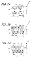
- FIG. 2A is a schematic top view of the TVS system, in a four-die embodiment.
- FIG. 2B is a schematic top view of the TVS system, with transverse die orientation.
- FIG. 2C is a schematic view of the TVS system, with a cross-pin lead configuration.
- FIG. 3A is a schematic diagram of the TVS system, in a unipolar embodiment.
- FIG. 3B is a schematic diagram of the TVS system, in a bipolar embodiment.
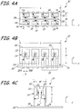
- FIG. 4A is a top view of the TVS system, in a sixteen-pin dual in-line package (DIP) configuration with surface-mount leads.
- DIP dual in-line package
- FIG. 4B is a side view of the TVS system, in a through-hole mount configuration.
- FIG. 4C is an end view of the TVS system, in the surface mount configuration.
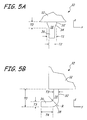
- FIG. 5A is an electrode detail for the through-hole configuration of FIG. 4B .
- FIG. 5B is an electrode detail for the surface mount configuration of FIG. 4C .
- FIG. 1A is a schematic side view of transient voltage suppression (TVS) system 10.
- System 10 comprises package 12, an array of TVS devices 14 comprising individual dies 15, and lead frame 16.
- the body of package 12 is typically manufactured from an insulating and heat resistant material such as a plastic polymer or ceramic, which is molded or formed around TVS devices 14 and lead frame 16.
- package 12 is formed as a shell and TVS dies 15 are attached to lead frame 16 and then inserted into package 12, which is then be filled with a potting compound or other insulating material.
- TVS devices 14 comprise semiconductor-based solid state electronics elements or dies 15, which operate as transient voltage suppressors or surge suppressors.
- Dies 15 are typically formed by thin-film deposition onto a substrate, with individual leads 18 connecting to the major parallel surfaces of each die 15.
- TVS devices 14 are arranged in one or more rows of four dies 15 each, with each die 15 oriented in a longitudinal sense along the inside of package 12.
- different numbers of TVS devices 14 are provided, for example between four and twenty-four, and dies 15 are arrayed either longitudinally or transversely within package 12, as described below.
- Lead frame 16 comprises a plurality of individual leads or pin electrodes 18. Leads 18 are arranged in pairs 18A, 18B, with leads from each pair connected to the opposite major surfaces of die 15.
- leads 18A and 18B extend from the major surfaces of dies 15 to adjacent pin locations along one side of package 12. Individual leads 18A are bonded to the front surface of each die 15 using lead bond or bond wire 19, and leads 18B are bonded to the back.
- TVS devices 14 are selected for relatively higher power capacity when used with exposed signal lines subject to direct transient signal sources, and relatively lower capacity for less exposed lines, which are primarily subject to indirectly induced transients.
- high-power TVS devices 14 utilize dies 15 with power ratings of 3 kW or more, for example about 3 kW, about 5 kW, about 10 kW or about 15 kW.
- TVS devices 14 utilize dies 15 with peak power ratings of 2 kW, 1 kW or less.
- TVS devices 14 In lightning suppression and other short-pulse width, high-amplitude applications, TVS devices 14 have a response time of 1-10 ⁇ s or less and are capable of peak power dissipation of at least 3 kW without thermal failure, internal sparking or shorting between input and output leads 18. Leads 18 have sufficiently low impedance to provide fast voltage clamping without excessive overshoot, and sufficient current carrying capacity to realize the given power rating and response time under a range of different operating conditions.
- the working voltage depends on the desired signal range and expected voltage surge conditions.
- different TVS devices 14 provide working voltage ranges including, but not limited to, 5 V, 6 V, 12 V, 18 V, 20 V, 24 V and 40 V.
- Voltage clamping is characterized by the rapid turn-on of a shunt current (rise time 1-10 ⁇ s or less) as the signal reaches the breakdown threshold.
- the shunt current dissipates pulse energy and clamps the peak voltage at approximately the breakdown potential, preventing transient spikes from propagating downstream, where they could damage sensitive electronics.
- System 10 provides this protection in a high-power, space-efficient, multiple-TVS package 12, offering fast, reliable transient suppression for avionics systems and other applications subject to high levels of vibration and temperature-induced stress, as described below.
- FIG. 1B is a schematic top view of TVS system 10.
- eight individual TVS devices 14 are arranged within package 12, in two rows of four dies 15 each.
- the rows of dies 15 are separated by spacer layer or insulator 20.
- dies 15 are bonded to opposite surface of spacer 20, and in other embodiments spacer 20 comprises a substrate on which dies 15 are formed.
- spacer 20 is inserted between two or more rows of TVS dies 15, as shown in FIG. 1 B , or between individual TVS devices 14.
- the material of package 12 provides an insulating layer or gap between rows of dies 15, or between individual TVS devices 14.
- FIG. 1C is a schematic end view of TVS system 10.
- TVS devices 14 are vertically oriented within package 12, with the major surfaces of each die 15 substantially perpendicular to top and bottom surfaces 22 and 24.
- the vertical orientation of TVS devices 14 substantially reduces surface area requirements for system 10, as compared to horizontally-mounted designs.
- the opposing major surfaces of each TVS die 15 are substantially perpendicular with respect to the horizontal plane of package 12, as defined by bottom surface 24.
- Leads 18 are connected to opposite major surfaces of each TVS die 15, either by soldering or other direct connection, or using lead bonds 19 as described above.
- TVS devices 14 within package 12 provides substantial size and weight savings for transient voltage suppression system 10, but also raises power management, temperature and vibration issues.
- thermal power management is a critical design issue because TVS dies 15 are more closely spaced in system 10 than in other, larger-area and discrete-element designs.
- Vibration control is also a critical design issue because the vertical array of TVS dies 15 changes the normal mode characteristics of package 12, as compared to discrete and horizontally-mounted embodiments.
- TVS elements 14 and lead frame 16 within package 12 This allows system 10 to be adapted to a range of high vibration, high temperature cycling environments and applications, including, but not limited to, avionics systems for fixed-wing and rotary-wing aircraft.
- FIG. 2A is a schematic top view of TVS system 10, with four TVS devices 14 housed in an eight-pin package 12.
- Package length L is defined in the longitudinal direction, along the two rows of leads 18, and package width W is defined in the transverse direction, across the two rows of leads 18.
- Package length L is generally greater than, or at least as great as, package width W.
- TVS devices 14 are arranged in a two by two matrix of dies 15.
- Each die 15 is arranged vertically within package 12 and longitudinally with respect to lead frame 16; that is, with major surfaces oriented along length L of package 12.
- FIG. 2B is a schematic top view of TVS system 10, with transverse die orientation.
- TVS devices 14 are arranged in a single row (or one-dimensional array) of four individual dies 15, with major surfaces substantially perpendicular or transverse to package length L, and oriented across package width W.
- FIG. 2C is a schematic top view of TVS system 10, with cross-pin lead pairs 18A and 18B.
- TVS devices 14 are vertically arranged in a single row or one-dimensional matrix, with transverse orientation for each die 15.
- lead frame 16 is arranged to connect TVS devices 14 across opposing lead pairs 18A and 18B, on opposite sides of package 12.
- Cross-pin lead configurations are also applicable to longitudinal die orientations and sixteen-pin packages 12. More generally, TVS system 10 encompasses embodiments with each of the variations described herein, either alone or in combination. In addition, system 10 is not limited to any particular eight or sixteen-pin embodiment of package 12, where lead frame 16 encompasses different numbers of leads 18, including, but not limited to, four-pin, ten-pin, fourteen-pin, twenty-pin, and twenty-four pin configurations.
- FIG. 3A is a schematic diagram of TVS system 10, in a unipolar (unidirectional) embodiment.
- Dies D1-D8 are electrically isolated inside package 12, with first and second major surfaces attached to separate pairs of leads 18 in lead frame 16. Outside package 12, individual leads 18 connect to signals S1-S6 and S8, and to a chassis or ground plane.
- TVS devices 14 are utilized to suppress remaining transients, shunting current to the ground plane and clamping the signal line voltage to protect downstream electronics.
- TVS devices 14 provide clamping capability for either positive or negative voltage surges on signal lines S1-S6 and S8, depending on the signal and ground connections to lead frame 16.
- signal lines S1-S6 are connected in a simple shunt-type arrangement, with each die D1-D6 connecting to a single signal line on one end, and to the ground plane or chassis on the other.
- Signals S1-S4 are connected in a positive or forward sense across dies D1-D4, and operate at positive voltages below the working voltage. When a lightning surge or other potentially damaging transient exceeds the breakdown potential, current shunts TVS device 14 to ground, clamping the signal voltage dissipating the pulse energy.
- Signals S5 and S6 are connected in a backward or negative sense across dies D5 and D6, operating with negative signal amplitudes and shunting current when the signal drops below the negative of the breakdown threshold.
- Signal S8 is connected across dies D7 and D8 in series, increasing the effective working voltage and reducing heat dissipation in individual TVS devices 14 by dividing the shunt voltage (and power output) across dies D7 and D8.
- FIG. 3B is a schematic diagram of TVS system 10, in a bipolar embodiment.
- dies D1-D6 are connected individually along signals S1-S6, which operate at either positive or negative working voltages, as described above, and signal S8 is connected across dies D7 and D8 in series.
- system 10 provides voltage clamping and transient suppression for a range of different signal configurations.
- system 10 is applicable to both single-ended and differential signal lines S1-S6 and S8, with either voltage-based or current-based signal protocols and both positive or negative signal conventions.
- FIG. 4A is a top view of TVS system 10, in a sixteen-pin embodiment with dual in-line package 12.
- Dual-in line package (DIP) 12 forms a substantially rectangular or oblong housing for the array of TVS devices 14, which are arranged on lead frame 16 with dies 15 in a vertical and longitudinal orientation.
- Package 12 is formed of a temperature-resistant insulating material such as a high-temperature thermoplastic or ceramic.
- the package material is formed or molded about TVS devices 14 and lead frame 16, producing multiple-TVS system 10 with an array of vertically oriented dies 15.
- TVS devices 14 are vertically oriented within package 12 to reduce surface area in the horizontal x-y plane. Dies 15 are also independently connected to lead frame 16 using separate leads 18, without internal cross-connections. This limits potential failure modes to individual dies 15, so that one short or other failure does not readily propagate to other TVS devices 14.
- TVS devices 14 are arranged in two longitudinal rows of four dies 15 each, separated by insulating layer or substrate 20.
- dies 15 are transversely oriented, as described above, or arranged in a single row or one-dimensional array.
- lead frame 16 comprises sixteen individual pin electrodes or leads 18, with pairs of adjacent leads connected across each of the eight TVS devices 14. Leads 18 are numbered in a counterclockwise sense, with pins P1 to P8 arranged sequentially along one side of package 12, and pins P9 to P16 on the other. In some embodiments, pin P1 is indicated by forming notch 26 or dot 28 on the top surface of package 12. In other embodiments, the pin numbering and identification scheme vary.
- FIG. 4B is a side view of TVS system 10, in a sixteen-pin DIP embodiment with through-hole electrode frame 16.
- Leads 18 are connected to opposite surfaces of each TVS device 14, with dies 15 oriented in a longitudinal direction along length L of package 12, between top surface 22 and bottom surface 24.
- the major surfaces of dies 15 are oriented in the vertical x-z plane, as opposed to the vertical y-z plane for transverse embodiments.
- Lead pairs 18A, 18B of lead frame 16 extend down through bottom surface (or bottom plane) 24 to adjacent pin locations along one side of package 12.
- leads 18 extend in a substantially vertical sense (along the z direction) to accommodate a through-plated solder connection to electronics board or chassis 30.
- package 12 is socket-mounted, or leads 18 may be bent for surface mounting as described below with respect to FIG. 4C .
- Adjacent lead spacing S is generally uniform, for example with a 0.10 inch or 100 mil (2.54 mm) pitch.
- the pitch is larger or smaller, including 0.20 inch or 200 mil (5.08 mm) pitch arrangements for larger, typically higher-power TVS devices 14, and 0.05 inch or 50 mil (1.27 mm) "half-pitch" arrangements for smaller, typically lower-power TVS devices 14.
- Metric pitches are also utilized, including 2.5 mm (0.098 inch), 5 mm (0.197 inch) and 8 mm (0.315 inch), with smaller pitches ranging from 0.5 mm (0.0197 inch) to 1.0 mm (0.039 inch) or 1.25 mm (0.049 inch), and larger pitches ranging up to 10 mm (0.394 inch) or more.
- FIG. 4C is an end view of TVS system 10, in a surface mount configuration.
- pin leads 18 are bent from the vertical (z) direction into the horizontal x-y plane, in order to accommodate surface-mount solder connections to electronics board or chassis 30.
- Vertical TVS elements 14 are shown in a longitudinal orientation, with the major surfaces of dies 15 aligned along package height H in the vertical x-z plane.
- TVS elements 14 and dies 15 depend on the location of system 10 within a particular electronics application, the vertical and horizontal planes of FIGS. 4A-4C are defined according to the features of package 12.
- TVS devices 14 are vertically oriented with respect to horizontal plane x-y of package 12, as defined by lead frame 16 and top and bottom surfaces 22 and 24.
- each die 15 are oriented along the vertical z-axis and in the direction of package height H, substantially perpendicular to horizontal plane x-y and top and bottom surfaces 22 and 24.
- the major surfaces of dies 15 are oriented in the vertical x-z plane, along package length L, and in transverse embodiments the major surfaces of dies 15 are oriented in the vertical y-z plane, across package width W.
- these vertical-mount configurations substantially reduce the surface area requirements of system 10 in the horizontal or x-y plane.
- lead frame 16 provides substantially more robust leads 18 than other designs, in order to more effectively dissipate heat from TVS devices 14 and package 12. Leads 18 also provide greater bonding strength in both surface mount and through-hole configurations, and robust lead frame 16 stiffens the mechanical structure of package 12 to resist temperature and vibration-induced stresses in operating environments subject to high levels of vibration and temperature cycling.
- FIG. 5A is an electrode detail for lead 18 of TVS system 10, in a through-hole or through-plated mounting configuration.
- Lead 18 is typically formed of a conducting material such as copper, with a coating such as hot-dipped tin/lead to prevent oxidization and facilitate solder or socket-type electrical connections.
- a coating such as hot-dipped tin/lead to prevent oxidization and facilitate solder or socket-type electrical connections.
- Other low resistivity metals are also used, and the contact surfaces are sometimes plated with conductors such as silver or gold, or left unplated.
- lead 18 is oriented in a substantially vertical sense along the z axis, with top collar portion 32, middle shoulder or neck-down portion 34, and bottom connecting or mounting portion 36.
- Top collar portion 32 has width T1 along the longitudinal x axis, where width T1 is typically greater than the diameter of the through-plated hole in order to provide washout spacing T0 between the bottom surface of package 12 and the circuit board.
- Neck-down portion 34 of lead 18 transitions from width T1 in top collar portion 32 to width T2 in bottom mounting portion 36, where width T2 is typically of smaller diameter to enable through-hole solder connections to a circuit board, or to insert lead 18 into a chip socket.
- FIG. 5B is an electrode detail for lead 18 of TVS system 10, in a surface mount configuration.
- lead 18 has bend 38 below top portion 32, with radius of curvature R selected to orient bottom mounting portion 36 in the horizontal (x-y) plane for surface-mount connection to a circuit board.
- Lead 18 has thickness T3 in mounting portion 36, and surface mount attachment length T4.
- connecting leads 18 provide thermal power management and vibration control features.
- leads 18 are substantially thicker and more robust than other pin designs, in order to dissipate thermal energy (heat) from TVS elements 14, and to resist vibration and temperature-induced stresses on package 12.
- lead 18 has width T1 of at least 0.040 inches (or about 1.016 mm) in collar portion 32.
- lead 18 has collar width T1 of at least 0.050 inches (1.27 mm), or at least 0.060 inches (1.524 mm).
- lead 18 has width T1 of at least 0.060 ⁇ 0.005 inches (1.524 ⁇ 0.127 mm) in collar portion 32.
- Lead 18 has width T2 in mounting portion 36.
- width T2 is at least 0.020 inches (or about 0.508 mm), at least 0.030 inches (0.762 mm), or at least 0.040 inches (1.016 mm).
- lead 18 has width T2 of at least 0.035 ⁇ 0.005 inches (0.889 ⁇ 0.127 mm) in mounting portion 36.
- Lead 18 also has thickness T3 in mounting portion 36, where thickness T3 is transverse to width T2.
- thickness T3 is at least 0.015 inches (or about 0.381 mm), at least 0.020 inches (0.508 mm), or at least 0.030 inches (0.762 mm).
- lead 18 has thickness T3 of at least 0.020 ⁇ 0.005 inches (0.508 ⁇ 0.127 mm) in mounting portion 36.
- Surface-mount attachment length T4 in mounting portion 36 also varies, for example in a range of at least 0.050 inches (or about 1.270 mm) or more. Alternatively, surface-mount attachment length T4 is at least 0.065 ⁇ 0.005 inches (1.651 ⁇ 0.127 mm).
- washout spacing T0 is about 0.030 ⁇ 0.005 inches (or about 0.762 ⁇ 0.127 mm) in through-plated configurations, or at least 0.020 inches (0.508 mm). In surface mount embodiments, washout spacing T0 is about 0.060 ⁇ 0.005 inches (1.524 ⁇ 0.127 mm), in order to position bend or curvature region 38 outside of neck-down or transition portion 34 on lead 18, or at least 0.050 inches (1.27 mm).
- Peak signal voltage and current depend on the relative exposure of the signal network, shielding configuration, and transient signal induction geometry. Generally, signal lines near a wing, nose, fuselage or rotor surface are subject to larger transients, because these surfaces are subject to direct attachment, and both magnetic and potential coupling occurs. The current path is also a critical variable, and widely-distributed flight control systems may require greater levels of transient voltage protection than other, more limited-area avionics systems, which are restricted to particular sections of the aircraft.
- Design considerations are also different for engine-mounted FADEC systems, as typical of fixed-wing aircraft, and cockpit or nacelle-mounted systems, as typical of rotary-wing helicopters.
- Engine-mounted FADEC systems for example, are susceptible to aperture coupling and similar induced transients, and cockpit and cabin-mounted systems are susceptible to electromagnetic (Faraday) coupling through windows and other openings in the outer skin of the aircraft.
- Faraday electromagnetic
- composite structural materials tend to provide less inherent shielding than metals.
- Other relevant effects include high intensity radiated fields (HIRF), electromagnetic pulses (EMP), and other high-energy pulses from non-lightning sources.
- HIRF high intensity radiated fields
- EMP electromagnetic pulses
- TVS management is a highly complex and unpredictable art, in which even relatively minor changes and modifications may have unexpected consequences.
- the peak transient pulse voltage may range above 500 V, for example 750 V, 1,000 V, 1,500 V or more.
- the peak current varies accordingly, for example 500 A, 750 A, 1,000 A, 1,500 A or more, based on a nominal one-ohm signal impedance.
- the shunt current ranges from up to 600 A at a clamping voltage of 5 V, to around 150 A at a clamping voltage of 20 V.
- leads 18 provide TVS system 10 with the ability to dissipate heat without substantially increasing the temperature of package 12.
- Results are based on a single standard 10 ⁇ s ⁇ 1,000 ⁇ s test pulse with a rise time of 10 ⁇ s to a peak of 750 V, and a decay time or half-life of 1,000 ⁇ s (1 ms). Under these conditions, the temperature increase was no more than 2 °C when up to eight or more TVS elements in a single package 12 were subject to the same test pulse. For higher-magnitude peaks of up to 1,500 V, the corresponding temperature increase may be less than about 5° C.
- the test pulse is repeated at intervals of several milliseconds (e.g., 1-10 ms for up to ten pulses), over a range of about 100 ms.
- leads 18 provide TVS system 10 with similar thermal management capability, limiting the temperature increase of package 12 to less than 5 °C for 750 V pulses, or less than 10 °C for higher amplitude pulses of up to 1,500 V at peak.
- Actual power dissipation also varies based on signal size, package and die configuration, and operating temperature.
- the nominal thermal load may reach 24 kW.
- TVS devices 14 are typically de-rated, and the peak power dissipation may be reduced accordingly.
- system 10 also lowers the real-time operating temperature of package 12, reducing de-rating effects. This increases the actual or net power capacity under actual operating conditions, and may extend the qualification testing range to higher ambient temperatures.
- Leads 18 also provide vibration management by structurally stiffening package 12, and changing the natural mode distribution.
- SIP single in-line package
- the arrangement of multiple TVS devices in package 12 suppresses lower-order bending modes, including first-order flexing modes characterized by oscillation in and out of the vertical z axis.
- the use of multiple, robust leads 18 also stiffens the overall structure of TVS system 10, increasing other natural mode frequencies, including in-plane modes where package 12 vibrates back and forth in the horizontal (x-y) plane.
- the lowest-order natural vibration mode frequency for package 12 is above (greater than) 1,000 Hz, for example at least 1,500 Hz.
- robust lead frame 16 shifts the lowest-order mode frequency above 2,000 Hz, for example to at least 2,500 Hz, or at least 3,000 Hz.
- vibration and thermal management features have utility in a range of applications including fixed-wing and rotary-wing avionics systems, where lightning-induced transients are experienced in high vibration and thermal cycling environments.
- the robust configuration of leads 18 provides TVS system 10 and package 12 with improved power management and mechanical performance at temperatures ranging from -55 °C or less to +125 °C or more, and when subject to engine and rotor-induced vibrations at frequencies up to 1,000 Hz, up to 1,500 Hz, or up to 2,000 Hz or more.
Landscapes
- Lead Frames For Integrated Circuits (AREA)
Applications Claiming Priority (1)
| Application Number | Priority Date | Filing Date | Title |
|---|---|---|---|
| US12/987,219 US8638535B2 (en) | 2011-01-10 | 2011-01-10 | Vertical mount transient voltage suppressor array |
Publications (2)
| Publication Number | Publication Date |
|---|---|
| EP2475005A2 true EP2475005A2 (de) | 2012-07-11 |
| EP2475005A3 EP2475005A3 (de) | 2014-03-26 |
Family
ID=45524293
Family Applications (1)
| Application Number | Title | Priority Date | Filing Date |
|---|---|---|---|
| EP11196213.0A Withdrawn EP2475005A3 (de) | 2011-01-10 | 2011-12-30 | Senkrechte montagetransiente Spannungsunterdrückungsanordnung |
Country Status (2)
| Country | Link |
|---|---|
| US (1) | US8638535B2 (de) |
| EP (1) | EP2475005A3 (de) |
Families Citing this family (4)
| Publication number | Priority date | Publication date | Assignee | Title |
|---|---|---|---|---|
| US9042072B2 (en) * | 2012-03-30 | 2015-05-26 | General Electric Company | Method and system for lightning protection with distributed transient voltage suppression |
| CN103617953A (zh) * | 2013-12-12 | 2014-03-05 | 天津中环半导体股份有限公司 | 一种矩阵式瞬态抑制二极管的制造方法 |
| CN108807316B (zh) * | 2017-08-14 | 2020-07-10 | 苏州捷芯威半导体有限公司 | 半导体封装结构及半导体器件 |
| CN112867928B (zh) | 2018-07-17 | 2024-09-17 | 哈勃股份有限公司 | 用于电力分配系统装置的电压采集器 |
Family Cites Families (33)
| Publication number | Priority date | Publication date | Assignee | Title |
|---|---|---|---|---|
| DE1439244B2 (de) * | 1963-05-29 | 1971-06-09 | Siemens AG, 1000 Berlin u 8000 München | Verfahren zum herstellen von halbleiterbauelementen |
| US4600960A (en) * | 1979-09-17 | 1986-07-15 | General Semiconductor Industries, Inc. | Four terminal pulse suppressor |
| JPH0331020Y2 (de) * | 1985-06-17 | 1991-07-01 | ||
| DE3629106A1 (de) | 1985-09-18 | 1987-03-26 | Smiths Industries Plc | Vorrichtung zur verminderung elektromagnetischer interferenzen |
| US5041901A (en) * | 1989-05-10 | 1991-08-20 | Hitachi, Ltd. | Lead frame and semiconductor device using the same |
| US5103193A (en) | 1989-08-25 | 1992-04-07 | The Boeing Company | Apparatus and methods for simulating a lightning strike in an aircraft avionics environment |
| US5103289A (en) * | 1990-02-06 | 1992-04-07 | Square D Company | Dual sip package structures |
| US5142263A (en) | 1991-02-13 | 1992-08-25 | Electromer Corporation | Surface mount device with overvoltage protection feature |
| JP2936769B2 (ja) * | 1991-03-28 | 1999-08-23 | 日本電気株式会社 | 半導体装置用リードフレーム |
| US5189387A (en) | 1991-07-11 | 1993-02-23 | Electromer Corporation | Surface mount device with foldback switching overvoltage protection feature |
| US5201855A (en) | 1991-09-30 | 1993-04-13 | Ikola Dennis D | Grid system matrix for transient protection of electronic circuitry |
| US5291375A (en) * | 1991-09-30 | 1994-03-01 | Kabushiki Kaisha Toshiba | Printed circuit board and electric device configured to facilitate bonding |
| US5528079A (en) * | 1991-12-23 | 1996-06-18 | Gi Corporation | Hermetic surface mount package for a two terminal semiconductor device |
| US5337216A (en) * | 1992-05-18 | 1994-08-09 | Square D Company | Multichip semiconductor small outline integrated circuit package structure |
| US5367124A (en) * | 1993-06-28 | 1994-11-22 | International Business Machines Corporation | Compliant lead for surface mounting a chip package to a substrate |
| JP3130784B2 (ja) * | 1995-12-28 | 2001-01-31 | アルプス電気株式会社 | 電子部品の端子構造 |
| JP2002043730A (ja) * | 2000-07-24 | 2002-02-08 | Mitsubishi Electric Corp | 集積回路パッケイジの実装方法および集積回路パッケイジ実装基板 |
| US6664656B2 (en) | 2000-09-14 | 2003-12-16 | The Boeing Company | Aircraft electrical power distribution network |
| USD466485S1 (en) * | 2001-05-23 | 2002-12-03 | Shindengen Electric Manufactuturing Co., Ltd. | Semiconductor package |
| CA2366941C (en) * | 2002-01-02 | 2010-06-29 | Marzio Paride Pozzuoli | Power supply circuit for an intelligent eclectronic device |
| US6919625B2 (en) * | 2003-07-10 | 2005-07-19 | General Semiconductor, Inc. | Surface mount multichip devices |
| US7310573B2 (en) | 2004-04-13 | 2007-12-18 | Pratt & Whitney Canada Corp. | Method and apparatus for isolating aircraft equipment |
| US7350281B2 (en) | 2004-07-26 | 2008-04-01 | Hamilton Sundstrand Corporation | Method of protecting a capacitor |
| US7432836B2 (en) | 2006-08-01 | 2008-10-07 | Hamilton Sundstrand Corporation | Multiplexed signal conditioner |
| US7558036B2 (en) | 2006-08-23 | 2009-07-07 | Hamilton Sundstrand Corporation | High speed lightning regulator circuit with self test attributes |
| US7741706B2 (en) * | 2006-09-29 | 2010-06-22 | Microsemi Corporation | Plastic surface mount large area power device |
| US20090015978A1 (en) * | 2007-07-12 | 2009-01-15 | Clark O Melville | Non-inductive silicon transient voltage suppressor |
| US8354847B2 (en) * | 2007-08-15 | 2013-01-15 | Electrostatic Answers Llc | Electrometer with in-measurement range adjustment and methods thereof for measuring electrostatic charge |
| US7821111B2 (en) * | 2007-10-05 | 2010-10-26 | Texas Instruments Incorporated | Semiconductor device having grooved leads to confine solder wicking |
| US20090254888A1 (en) * | 2008-04-07 | 2009-10-08 | International Business Machines Corporation | Debug tours for software debugging |
| WO2009142657A1 (en) * | 2008-05-19 | 2009-11-26 | Polyphaser Corporation | Dc and rf pass broadband surge suppressor |
| US8023245B2 (en) | 2008-10-13 | 2011-09-20 | Hamilton Sundstrand Corporation | Lightning strike mitigation for aircraft |
| US8274164B2 (en) * | 2008-11-06 | 2012-09-25 | Microsemi Corporation | Less expensive high power plastic surface mount package |
-
2011
- 2011-01-10 US US12/987,219 patent/US8638535B2/en active Active
- 2011-12-30 EP EP11196213.0A patent/EP2475005A3/de not_active Withdrawn
Non-Patent Citations (1)
| Title |
|---|
| None |
Also Published As
| Publication number | Publication date |
|---|---|
| US8638535B2 (en) | 2014-01-28 |
| EP2475005A3 (de) | 2014-03-26 |
| US20120176716A1 (en) | 2012-07-12 |
Similar Documents
| Publication | Publication Date | Title |
|---|---|---|
| US9414532B2 (en) | Electronic power module arrangement | |
| US8638535B2 (en) | Vertical mount transient voltage suppressor array | |
| EP4106501A1 (de) | Kabelanordnung, signalübertragungsstruktur und elektronische vorrichtung | |
| CN103077938A (zh) | 用于瞬时电压抑制器的方法和系统 | |
| TWI327803B (en) | Circuit for preventing surge, connector and electronic apparatus thereof | |
| US10622287B2 (en) | Semiconductor package | |
| JP3940431B2 (ja) | 避雷装置 | |
| US10743406B2 (en) | Galvanic isolation for isolation transformer | |
| US20240096763A1 (en) | Package structure for asymmetric transient voltage suppressor | |
| CN107068312B (zh) | 一种具有空气放电结构的一体化盒装fdmov复合组件 | |
| Kosteletskii et al. | Development of a high current protection device against ultrashort pulse | |
| US11380631B2 (en) | Lead frame for multi-chip modules with integrated surge protection | |
| US3359360A (en) | Xelectronic c component assembly including a mounting bracket with removable loops | |
| US12260975B2 (en) | Over-voltage circuit protection device | |
| CN218896632U (zh) | 瞬态电压抑制单向器件 | |
| TWI591794B (zh) | 靜電放電保護元件 | |
| CN223487055U (zh) | 用于瞬态电压抑制器(tvs)器件的封装结构 | |
| CN223321264U (zh) | 用于高电流SIDACtor的封装结构 | |
| US12622278B2 (en) | Semiconductor package | |
| CN113078621B (zh) | 一种嵌入式mov组件 | |
| US5244416A (en) | Multicontact connector protected against interference | |
| CN218996453U (zh) | 一种贴片式并联压敏电阻器 | |
| KR102839039B1 (ko) | 모놀리식 다중 채널 보호 장치 | |
| CN214043647U (zh) | 表面贴装封装和表面贴装芯片封装的引线框架结构装置 | |
| US11751324B2 (en) | Electronic card comprising a first ground plane and a second ground plane |
Legal Events
| Date | Code | Title | Description |
|---|---|---|---|
| PUAI | Public reference made under article 153(3) epc to a published international application that has entered the european phase |
Free format text: ORIGINAL CODE: 0009012 |
|
| AK | Designated contracting states |
Kind code of ref document: A2 Designated state(s): AL AT BE BG CH CY CZ DE DK EE ES FI FR GB GR HR HU IE IS IT LI LT LU LV MC MK MT NL NO PL PT RO RS SE SI SK SM TR |
|
| AX | Request for extension of the european patent |
Extension state: BA ME |
|
| PUAL | Search report despatched |
Free format text: ORIGINAL CODE: 0009013 |
|
| RIC1 | Information provided on ipc code assigned before grant |
Ipc: H01L 21/56 20060101ALI20140213BHEP Ipc: H01L 23/62 20060101AFI20140213BHEP Ipc: H01L 23/49 20060101ALI20140213BHEP Ipc: H01L 23/31 20060101ALI20140213BHEP Ipc: H01L 23/495 20060101ALI20140213BHEP Ipc: H01L 23/16 20060101ALI20140213BHEP |
|
| AK | Designated contracting states |
Kind code of ref document: A3 Designated state(s): AL AT BE BG CH CY CZ DE DK EE ES FI FR GB GR HR HU IE IS IT LI LT LU LV MC MK MT NL NO PL PT RO RS SE SI SK SM TR |
|
| AX | Request for extension of the european patent |
Extension state: BA ME |
|
| RIC1 | Information provided on ipc code assigned before grant |
Ipc: H01L 23/495 20060101ALI20140217BHEP Ipc: H01L 21/56 20060101ALI20140217BHEP Ipc: H01L 23/62 20060101AFI20140217BHEP Ipc: H01L 23/31 20060101ALI20140217BHEP Ipc: H01L 23/16 20060101ALI20140217BHEP Ipc: H01L 23/49 20060101ALI20140217BHEP |
|
| STAA | Information on the status of an ep patent application or granted ep patent |
Free format text: STATUS: THE APPLICATION IS DEEMED TO BE WITHDRAWN |
|
| 18D | Application deemed to be withdrawn |
Effective date: 20140927 |