EP2476775A1 - Film de protection et son procédé de production - Google Patents
Film de protection et son procédé de production Download PDFInfo
- Publication number
- EP2476775A1 EP2476775A1 EP10815514A EP10815514A EP2476775A1 EP 2476775 A1 EP2476775 A1 EP 2476775A1 EP 10815514 A EP10815514 A EP 10815514A EP 10815514 A EP10815514 A EP 10815514A EP 2476775 A1 EP2476775 A1 EP 2476775A1
- Authority
- EP
- European Patent Office
- Prior art keywords
- protective film
- substrate
- film
- segments
- depositing
- Prior art date
- Legal status (The legal status is an assumption and is not a legal conclusion. Google has not performed a legal analysis and makes no representation as to the accuracy of the status listed.)
- Withdrawn
Links
Images




Classifications
-
- C—CHEMISTRY; METALLURGY
- C23—COATING METALLIC MATERIAL; COATING MATERIAL WITH METALLIC MATERIAL; CHEMICAL SURFACE TREATMENT; DIFFUSION TREATMENT OF METALLIC MATERIAL; COATING BY VACUUM EVAPORATION, BY SPUTTERING, BY ION IMPLANTATION OR BY CHEMICAL VAPOUR DEPOSITION, IN GENERAL; INHIBITING CORROSION OF METALLIC MATERIAL OR INCRUSTATION IN GENERAL
- C23C—COATING METALLIC MATERIAL; COATING MATERIAL WITH METALLIC MATERIAL; SURFACE TREATMENT OF METALLIC MATERIAL BY DIFFUSION INTO THE SURFACE, BY CHEMICAL CONVERSION OR SUBSTITUTION; COATING BY VACUUM EVAPORATION, BY SPUTTERING, BY ION IMPLANTATION OR BY CHEMICAL VAPOUR DEPOSITION, IN GENERAL
- C23C16/00—Chemical coating by decomposition of gaseous compounds, without leaving reaction products of surface material in the coating, i.e. chemical vapour deposition [CVD] processes
- C23C16/04—Coating on selected surface areas, e.g. using masks
- C23C16/042—Coating on selected surface areas, e.g. using masks using masks
-
- C—CHEMISTRY; METALLURGY
- C23—COATING METALLIC MATERIAL; COATING MATERIAL WITH METALLIC MATERIAL; CHEMICAL SURFACE TREATMENT; DIFFUSION TREATMENT OF METALLIC MATERIAL; COATING BY VACUUM EVAPORATION, BY SPUTTERING, BY ION IMPLANTATION OR BY CHEMICAL VAPOUR DEPOSITION, IN GENERAL; INHIBITING CORROSION OF METALLIC MATERIAL OR INCRUSTATION IN GENERAL
- C23C—COATING METALLIC MATERIAL; COATING MATERIAL WITH METALLIC MATERIAL; SURFACE TREATMENT OF METALLIC MATERIAL BY DIFFUSION INTO THE SURFACE, BY CHEMICAL CONVERSION OR SUBSTITUTION; COATING BY VACUUM EVAPORATION, BY SPUTTERING, BY ION IMPLANTATION OR BY CHEMICAL VAPOUR DEPOSITION, IN GENERAL
- C23C14/00—Coating by vacuum evaporation, by sputtering or by ion implantation of the coating forming material
- C23C14/04—Coating on selected surface areas, e.g. using masks
-
- C—CHEMISTRY; METALLURGY
- C23—COATING METALLIC MATERIAL; COATING MATERIAL WITH METALLIC MATERIAL; CHEMICAL SURFACE TREATMENT; DIFFUSION TREATMENT OF METALLIC MATERIAL; COATING BY VACUUM EVAPORATION, BY SPUTTERING, BY ION IMPLANTATION OR BY CHEMICAL VAPOUR DEPOSITION, IN GENERAL; INHIBITING CORROSION OF METALLIC MATERIAL OR INCRUSTATION IN GENERAL
- C23C—COATING METALLIC MATERIAL; COATING MATERIAL WITH METALLIC MATERIAL; SURFACE TREATMENT OF METALLIC MATERIAL BY DIFFUSION INTO THE SURFACE, BY CHEMICAL CONVERSION OR SUBSTITUTION; COATING BY VACUUM EVAPORATION, BY SPUTTERING, BY ION IMPLANTATION OR BY CHEMICAL VAPOUR DEPOSITION, IN GENERAL
- C23C14/00—Coating by vacuum evaporation, by sputtering or by ion implantation of the coating forming material
- C23C14/04—Coating on selected surface areas, e.g. using masks
- C23C14/042—Coating on selected surface areas, e.g. using masks using masks
-
- C—CHEMISTRY; METALLURGY
- C23—COATING METALLIC MATERIAL; COATING MATERIAL WITH METALLIC MATERIAL; CHEMICAL SURFACE TREATMENT; DIFFUSION TREATMENT OF METALLIC MATERIAL; COATING BY VACUUM EVAPORATION, BY SPUTTERING, BY ION IMPLANTATION OR BY CHEMICAL VAPOUR DEPOSITION, IN GENERAL; INHIBITING CORROSION OF METALLIC MATERIAL OR INCRUSTATION IN GENERAL
- C23C—COATING METALLIC MATERIAL; COATING MATERIAL WITH METALLIC MATERIAL; SURFACE TREATMENT OF METALLIC MATERIAL BY DIFFUSION INTO THE SURFACE, BY CHEMICAL CONVERSION OR SUBSTITUTION; COATING BY VACUUM EVAPORATION, BY SPUTTERING, BY ION IMPLANTATION OR BY CHEMICAL VAPOUR DEPOSITION, IN GENERAL
- C23C16/00—Chemical coating by decomposition of gaseous compounds, without leaving reaction products of surface material in the coating, i.e. chemical vapour deposition [CVD] processes
- C23C16/04—Coating on selected surface areas, e.g. using masks
-
- C—CHEMISTRY; METALLURGY
- C23—COATING METALLIC MATERIAL; COATING MATERIAL WITH METALLIC MATERIAL; CHEMICAL SURFACE TREATMENT; DIFFUSION TREATMENT OF METALLIC MATERIAL; COATING BY VACUUM EVAPORATION, BY SPUTTERING, BY ION IMPLANTATION OR BY CHEMICAL VAPOUR DEPOSITION, IN GENERAL; INHIBITING CORROSION OF METALLIC MATERIAL OR INCRUSTATION IN GENERAL
- C23C—COATING METALLIC MATERIAL; COATING MATERIAL WITH METALLIC MATERIAL; SURFACE TREATMENT OF METALLIC MATERIAL BY DIFFUSION INTO THE SURFACE, BY CHEMICAL CONVERSION OR SUBSTITUTION; COATING BY VACUUM EVAPORATION, BY SPUTTERING, BY ION IMPLANTATION OR BY CHEMICAL VAPOUR DEPOSITION, IN GENERAL
- C23C16/00—Chemical coating by decomposition of gaseous compounds, without leaving reaction products of surface material in the coating, i.e. chemical vapour deposition [CVD] processes
- C23C16/22—Chemical coating by decomposition of gaseous compounds, without leaving reaction products of surface material in the coating, i.e. chemical vapour deposition [CVD] processes characterised by the deposition of inorganic material, other than metallic material
- C23C16/26—Deposition of carbon only
-
- Y—GENERAL TAGGING OF NEW TECHNOLOGICAL DEVELOPMENTS; GENERAL TAGGING OF CROSS-SECTIONAL TECHNOLOGIES SPANNING OVER SEVERAL SECTIONS OF THE IPC; TECHNICAL SUBJECTS COVERED BY FORMER USPC CROSS-REFERENCE ART COLLECTIONS [XRACs] AND DIGESTS
- Y10—TECHNICAL SUBJECTS COVERED BY FORMER USPC
- Y10T—TECHNICAL SUBJECTS COVERED BY FORMER US CLASSIFICATION
- Y10T428/00—Stock material or miscellaneous articles
- Y10T428/24—Structurally defined web or sheet [e.g., overall dimension, etc.]
- Y10T428/24802—Discontinuous or differential coating, impregnation or bond [e.g., artwork, printing, retouched photograph, etc.]
Definitions
- the present invention relates to protective films having segmented shapes, obtained by depositing films to be divided into segments, and in particularly a diamond-like carbon (DLC) protective film, and to methods for producing the protective films.
- DLC diamond-like carbon
- a technology for coating on a material surface a hard film that has long life and high reliability and can be used in a carefree manner has been sought, as a protective film for mechanical components or the like.
- a hard carbon film particularly diamond-like carbon (DLC)
- DLC diamond-like carbon
- DLC is a material that contains carbon as a main component, is generally amorphous while carbon atoms have graphite sp 2 bonds and diamond sp 3 bonds, and exhibits intermediate physical properties between graphite and diamond.
- Patent Literature 1 a protective film having a segmented shape, wherein a film formed divided into segments is deposited on a substrate.
- Patent Literature 1 It is known that, to obtain such a protective film having a segmented shape, a substrate is masked using a wire gauze of a tungsten wire or the like and a protective film is thereafter deposited (Patent Literature 1). More specifically, the parts corresponding to wire gauze meshes constitute segments by performing masking using a wire gauze of a tungsten wire or the like, a lattice-shaped segmented film is obtained, and wire gauze parts, namely, the parts corresponding to the net wires of the wire gauze constitute spacings between adjacent segments.
- a segmented shape by masking using a wire gauze is limited by the processability (degree of freedom) of the wire gauze.
- a film deposited in the meshes of the wire gauze may only have a constant thickness.
- the meshes of an ordinary wire gauze are uniform, the shapes of segments are difficult to change correspondingly to the portion on which a film is formed.
- even masking by a wire gauze can be relatively easily applied when a substrate to be masked is planar while the application of the masking by the wire gauze is difficult when the substrate has a three-dimensional shape.
- Objects of the present invention are: to provide a DLC film, wherein a protective film having a segmented shape is easily formed, quality control of the protective film is improved, segmented shapes with a high degree of freedom (that are complicated) are possible, and the application of the DLC film is possible not only to two-dimensional shapes but also to three-dimensional shapes; and to provide a method for forming the DLC film.
- a DLC film wherein a protective film having a segmented shape is easily formed, quality control of the protective film is improved, segmented shapes with a high degree of freedom (that are complicated) are possible, and the application of the DLC film is possible not only to two-dimensional shapes but also to three-dimensional shapes; and a method for forming the DLC film are provided.
- the protective film according to the present invention is characterized by, when forming on a substrate the protective film having a segmented shape formed by depositing a film so that the film is formed divided into segments, masking the substrate using a drawing material so that segments having predetermined shapes are obtained, thereafter depositing the protective film, and then removing the masked part to form a spacing between segments.
- an embodiment of the present invention is the protective film obtained by, when forming on a substrate the protective film having a segmented shape formed by depositing a film so that the film is formed divided into segments, groove-processing the substrate using a cutting tool so that segments having predetermined shapes are obtained, and thereafter depositing the protective film to form a spacing between segments.
- the protective film according to the present invention is described in detail below. It is necessary that the protective film according to the present invention should have a segmented shape formed by depositing a film so that the film is formed divided into segments.
- the segments have shapes that are not particularly limited but may appropriately be selected from triangles, quadrangles, circles and the like.
- the segments have sizes that are usually selected from one side or an outside diameter of 1 ⁇ m to 3 mm.
- the spacing between adjacent segments is usually 0.1 ⁇ m to 1 mm.
- the segments usually have film thicknesses of 1 nm to 200 ⁇ m.
- the substrate is masked using the drawing material in sizes and shapes corresponding to segment spacing parts so that the segments having predetermined shapes are obtained.
- the drawing-masking may be performed by the drawing mechanism using various printing techniques such as handwriting, ink-jet printing, offset printing, gravure printing, flexographic printing, type printing, screen printing and photolithographic printing. Particularly, ink-jet printing or photolithographic printing is preferred. This is because the degree of freedom for change of masking condition is high and its application to a three-dimensional substrate is easy. Since a drawing (printing) pattern may freely be set, i.e., a different segment pattern may be applied on each substrate, the protective film having an optimal segment structure depending on its application can be obtained.
- the possibility of setting the drawing (printing) pattern means that marking or naming can also be performed using the protective film with a segmented structure.
- Contact-drawing (contact-printing) of the substrate enables marking or name-removal by removing (peeling) the drawing material after formation of the film.
- the width and bending manner of a groove after removal of the drawing material can also freely be controlled, and the groove can also easily be used as a flow path.
- a thickness may be adjusted. The thickness can be adjusted by, e.g., coating several layers of the drawing materials, and, thereby, the thickness of the accumulated film can also be changed.
- a mesh may optionally be changed, and a fine segmented structure and a large segmented structure may gradationally be set. This makes it possible to change a light transmission level in the protective film.
- a pattern (figure), a film thickness and a gradation may also freely be combined.
- the drawing material is appropriately selected in consideration of safety, keeping quality, application properties (such as degrees of adhesion, repellency, bleeding and wetting to an opposite material) and the like.
- a drawing material (ink) for ink-jet printing a pigment is recommended to have a size of about 1 ⁇ m or less and a viscosity of about 3 mPa ⁇ s or less.
- the ink may also be supplied from an ink tank, or, when the ink is easy to deposit, a mechanism that stirs or the like so that the ink becomes in an appropriately mixed state prior to drawing (printing) may also be included.
- the drawing material may also contain a conductive material.
- the conductive material are carbon-containing materials, ITO inks and the like.
- the drawing material containing a conductive material may be utilized as a conductive path when an electric action is utilized during forming a film.
- an electric resistivity is desirably 10 5 ⁇ ⁇ m or less. This is because the electric resistivity ensures conductivity when a voltage of 3 kV or more is applied.
- the drawing material may contain a semiconductor material or an insulating material.
- the semiconductor material are polymeric materials containing polycrystalline silicon
- examples of the insulating material are polymeric materials containing silica particles.
- the drawing material preferably has an electric resistivity ranging from 10 5 -10 6 ⁇ ⁇ m in the case of the semiconductor whereas the drawing material preferably has an electric resistivity ranging from 10 6 -10 17 ⁇ ⁇ m in the case of the insulating material.
- the function of the drawing material as an auxiliary electrode is decreased to inhibit an electric current from passing and to decrease a film formation rate, with increasing the electric resistivity of the drawing material, when a DLC film is formed, while increase in the temperature of the substrate can be suppressed, and therefore the drawing material having a suitable electric resistivity can be selected in consideration of the heat resistance of the substrate.
- the drawing material may also contain a resist material.
- the resist material which is a photosensitive polymeric material, is cured by a beam generated by a light irradiation (drawing) mechanism such as a laser drawing apparatus or an electron beam drawing apparatus.
- a light irradiation (drawing) mechanism such as a laser drawing apparatus or an electron beam drawing apparatus.
- a resist layer is formed.
- the resist layer is irradiated with a beam, the part that has been irradiated with the beam is cured whereas the part that has not been irradiated with the beam is not cured.
- the part that is not cured can be removed by chemical cleaning. After the removal of the non-cured portion (non-irradiated portion), a mask pattern is formed.
- the resist material are a positive type resist including a novolac resin and a diazonaphthoquinone (DNQ) compound, and the like.
- a substrate may also be groove-processed using a cutting tool, in place of the masking with the drawing material, followed by depositing the protective film to form a spacing between segments.
- the width of the groove is selected from the range of 0.1 ⁇ m to 1 mm, the spacing of adjacent segments.
- the depth of the groove by the cutting tool is selected from the range of around 2 ⁇ m to 2 mm. This is because it is currently difficult to uniformly introduce a groove of 2 ⁇ m or less due to cutting precision, the lower limit is therefore around 2 ⁇ m, and a groove depth of 2 mm or more causes significant deformation due to the shearing stress of a convex part (namely segmented part) to deteriorate characteristics in the protective film.
- the cross-sectional shape of the groove is optional and is selected from, e.g., a V-shape, a U-shape, etc.
- an appropriate conventional tool may be used depending on the material of the substrate and the desired dimension and shape of the groove, and, for example, a dicer, a diamond micro-router or the like may be used. Only a groove depth corresponding to a film thickness, or equivalently, a groove depth of several nanometers to several hundred micrometers can be obtained in the protective film having a segmented structure made by being masked with the drawing material while a groove with a depth of around 1 mm can easily be made according to this method of groove-processing the substrate using the cutting tool.
- the protective film deposited after the groove-processing of the substrate is divided by grooves to obtain the protective film having a segmented shape.
- the protective film having a segmented structure, formed on the substrate with a groove having a depth of 1 mm has around 1.5 times improved wear resistance in comparison with the protective film made by being masked with the drawing material. This is because stress applied to the film is decreased by performing the groove-processing.
- the effect of the groove-processing is high in the case of a comparatively low load of 1 N or less while no cutting is more effective in the case of a sphere of 6 mm in diameter and a vertical load of 1 N or more. This is because the substrate per se is deformed by applying cutting. Since trapping of an abrasion powder in a groove is effective for suppressing abrasive wear (a damaged protective film as a friction agent attacks the remaining protective film to accelerate wear), the protective film having deep grooves made by this method is effective when severe abrasive wear occurs.
- this method is not appropriate but it is appropriate to use the protective film having a segmented structure made by being masked with the drawing material, when a vertical load (force applied to a protective film by an opposite material) is large during sliding, or specifically, when applied force equivalent to 1/10 or more of the yield stress of the substrate is applied.
- Substrates used in accordance with the present invention are not particularly limited but include, for example, metals such as aluminum, magnesium, alloys thereof and steel; plastics; rubbers; ceramics; composite materials thereof; and the like, and may appropriately be selected depending on a purpose.
- the surface of the substrate on which the protective film is deposited may have a three-dimensional shape.
- the three-dimensional shape is a plane, particularly a curved plane, made by plasticity processing such as machine processing or press processing, casting, or the like.
- processing such as machine processing, electrical-discharge processing, hand work or abrasive finishing is also used.
- These planes are defined as three-dimensional shapes as used herein.
- a brass cast product is finished by machine processing and details are subjected to hand work.
- convex and concave lenses are subjected to abrasive finishing, and aspherical lenses are subjected to casting + abrasive finishing.
- the protective film according to the present invention can be deposited on such various, complicated three-dimensional shapes.
- a film is deposited.
- the film is deposited on an unmasked spot to obtain the segment-shaped protective film.
- No film is deposited on a masked part, which constitutes a spacing between adjacent segments.
- a film is deposited after the groove-processing of the substrate.
- a vapor phase deposition method is preferably applied as a protective film deposition method, of which examples include plasma CVD with a direct-current power source, an alternating-current power source, a high frequency power source, a pulsed power source or the like as a power source, or a sputtering method such as magnetron sputtering or ion beam sputtering.
- a protective film deposition method of which examples include plasma CVD with a direct-current power source, an alternating-current power source, a high frequency power source, a pulsed power source or the like as a power source, or a sputtering method such as magnetron sputtering or ion beam sputtering.
- Illustrated is the scheme of the apparatus equipped with a chamber 5, an exhaust system 10 (a rotary pump 11, a turbo molecular pump 12, a vacuum gauge 13, an exhaust valve 14, etc.), a gas introduction system 15 (a valve for introducing gases such as Ar, C 2 H 2 , Si (CH 3 ) 4 ), H 2 , O 2 , N 2 , CH 4 and CF 4 ) and a power source system 20 (main power source 16, a substrate heating power source 17, a fine particles trapping filter power source 18, a surplus electrons collecting power source 19 and the like).
- Fig. 2 The scheme of the mechanism that forms a protective film on a substrate in the apparatus according to Fig. 1 is illustrated in Fig. 2 .
- the substrate is placed on an electrode in a chamber in this apparatus, and the substrate is masked. Air is exhausted from the inside of the chamber by an evacuation mechanism after the placing of the substrate, plasma gas sources, Ar, Si(CH 3 ) 4 , C 2 H 2 and the like are then supplied, a pulsed voltage is applied by a pulsed power source, and the plasma gas sources are made to be plasma.
- the gas made to be the plasma is deposited on the substrate using the masking to obtain the protective film having a segmented shape.
- the deposited protective film may preferably be imparted with wear resistance and may contain any or a combination of, e.g., diamond, diamond-like carbon, BN, W 2 C, CrN, HfN, VN, TiN, TiCN, Al 2 O 3 , ZnO and SiO 2 films.
- the thicknesses of these films are selected usually from 1 nm to 200 ⁇ m.
- a masked part is removed.
- the masked part (drawing material) can be removed without damaging the substrate by appropriate physical and chemical procedures.
- the physical removal methods for example, sandpaper and sandblast can be used.
- the chemical removal methods include, for example, a method of dissolution by a solvent that is appropriately selected depending on a drawing material.
- the protective film having a segmented shape in accordance with the present invention a corner between the top and side of each segment (shoulder of each segment), which corner is not sharp but is round, is obtained. More specifically, 95% or more of the corner is curved with a radius of curvature that is not less than the film thickness of the protective film. This is because the protective film is deposited via the masking, flying of deposited film components (carbon and the like) is therefore blocked by the masked substrate part and the vicinity thereof, and consequently the corner that is not sharp but is round is obtained.
- the protective film having the segmented shape that is gently round is used in a mechanical component, particularly in the sliding plane thereof, effects of the stability of sliding friction and long life are shown.
- the protective film according to the present invention may be produced using an articulated robot with a drawing mechanism.
- the articulated robot is generally equipped with shafts of which the number is four, five or six.
- the number of the shafts indicates the number of rotation articulations, and, with increasing the number of the articulations, the number of movable units is increased to increase the degree of the freedom of the posture of an operation unit (generally placed on the top of an arm).
- the operation unit of the articulated robot is equipped with the drawing mechanism. Examples of the drawing mechanism are writing instruments, the printer heads of ink-jet printers, and the like.
- the masking-drawing of the substrate is performed by linking or collaboration between the working of the arm of the articulated robot and the drawing operation by the drawing mechanism.
- a tank in which a drawing material (ink) is put may also be placed in the vicinity of the drawing mechanism and is preferably placed in the location that does not interfere with printing and the movement of the arm.
- the drawing material is supplied to the drawing mechanism on the basis of an ink-jet system.
- the scheme of the articulated robot that drawing-masks the substrate is illustrated in Fig. 3 .
- the accuracy of the position of a robot is ⁇ 0.08 mm (80 ⁇ m) and the thickness of a drawn line is 50 ⁇ m ⁇ 10 ⁇ m, 80 + 10 ⁇ 100 ⁇ m (0.01 mm) can be regarded as the precision of the drawn line even if the thickness of the line is varied with a distance between a matter to be printed and the drawing mechanism (head).
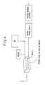
- the robot arm is at P 0 (home position) in an initial state. Instructions of moving of the arm and an event (working) at each point (P) are selected by operating each button of a teaching box, to perform input. This sequence is repeated, and E.O.P. (end-of-program) is input to complete a program.
- the arm need not be located at the home position at the time of E.O.P.
- the ink-jet printer includes a printing mechanism including: ink discharge nozzles; a driver (power source) that makes and stops the nozzles discharge of ink; pattern drawing software that gives a drawing instruction to the driver; an ink cartridge (ink tank) for supplying ink; and the like.
- the printer head may also be installed on the top of the robot arm to fit the working reference point of the robot arm (three-dimensional movement mechanism). The arrangement of the ink discharge nozzles and the movement of the robot arm can be adjusted to adopt coordinates of which the X-Y directions are common.
- Ink is supplied to the printer heads, discharged from the nozzles and sprayed on an object (substrate) to draw a desired pattern, according to the instruction from the driver.
- a cutting tool for groove-processing may also be installed in place of the printer head.
- a process flow of drawing-masking is illustrated in Fig. 5 .
- a) The substrate (workpiece) is set in a jig, b) a drawing instruction is given to the robot (three-dimensional movement mechanism), c) the robot makes the ink-jet head approach a predetermined location in the workpiece, and ink is discharged from the inkjet to draw a desired pattern, d) the substrate (workpiece) is transferred (together with a jig cassette) to a drying step, e) the ink on the substrate (workpiece) is dried, and the dried and adhered ink becomes a mask, f) a film is then produced, and g) a protective film having a desired segmented shape is obtained by removing the mask after the production of the film.
- groove-processing may also be performed.
- a-f illustrate examples of planar drawn patterns
- g-j illustrate examples of three-dimensional drawn patterns
- a-f illustrates a mesh
- b illustrates a honeycomb-shaped mesh
- c illustrates lines between which pitches are varied
- d illustrates continuous circles linked by lines
- e illustrates all one color and a partially shaded area
- f illustrates a pattern.
- g illustrates the inner sides of a concave lens (aspherical surface, etc.)
- h illustrates a saddle-shaped surface
- i illustrates a three-dimensional parabola surface
- j illustrates a three-dimensional printed pattern on a sphere.
- FIG. 7A and Fig. 7B an embodiment in the case of using a resist material as a drawing material is illustrated.
- a light-irradiated portion of the resist layer can be cured to remain as a mask by irradiating the resist layer with light using a light irradiation mechanism made of an optical fiber, which light irradiation mechanism is mounted on the arm unit of the articulated robot.
- Fig. 7A is a view of a system for light exposure to a curved surface using a six-shaft robot and a laser or ultraviolet light source.
- Fig. 7B is a model view of irradiation. In the system according to Fig.
- a substrate can always be irradiated perpendicularly with light, for example, by movement of A ⁇ B ⁇ C ⁇ D ⁇ E. Only an irradiated resist may be cured to remain, thereby being able to use the resist as a mask during forming a DLC film.
- the present invention also relates to a method for producing the above-mentioned protective film according to the present invention.
- lattice-shaped lines were drawn on the surface of a sample (pipe) having the curved surface.
- the material of the substrate of the sample is stainless steel.
- a drawing material in which Ketjen black was dispersed in polymers was used.
- a locus on a curved surface was continuously formed on a program by arc compensation, parabola compensation and free-curve compensation using a teaching function (function of moving the top of a robot above an actual article (workpiece) to read a coordinate from the actual article (workpiece)) and was drawn so that the top of the arm of the robot was always perpendicular to a plane.
- a drawing speed was 30 mm/s.
- the drawing material was dried, followed by forming a DLC film by a pulsed plasma CVD method. Film formation conditions are described below.
- the polymer substrate of a drawn portion was dissolved in acetone or alcohol to realize the DLC film.
- the DLC film having a segmented structure was confirmed to be uniformly formed on the curved surface.
- a resist was applied to a substrate to have a thickness of about 50 ⁇ m by an ultrasonic or spin coater, and the substrate was irradiated by condensing light from YAG lasers (1.06 ⁇ m) of a pulsed Q-switch to 30 ⁇ m at the top through an optical fiber from the top of the six-shaft robot to cure the resist on the irradiated portion.
- a linear pattern was formed by scanning the lasers at spacings of 200-300 ⁇ m. Position control was performed by the robot in the same manner as in Example 1 so that the curved surface can always be irradiated with the lasers from equal distances.
- a grid structure was made by further similarly performing scanning in a straight direction.
- a non-irradiated portion was removed by a remover, and a DLC film was then formed under the conditions described below by a radio-frequency plasma CVD method. Thereafter, the DLC film having a segmented structure was obtained by lift-off of the resist.
- Grooves with a depth of 20 ⁇ m was lengthwise and crosswise digged by a dicer with a width of 20 ⁇ m for dicing a Si wafer while performing position-control by the robot in the same manner as in Example 1, ultrasonic cleaning with acetone was performed, and thereafter a DLC film was formed under the conditions described below to obtain the DLC film having a segmented structure.
- Grooves with a width of 20 ⁇ m and depths of 10-20 ⁇ m were made by a diamond micro router (grinding stone) while performing position-control by the robot in the same manner as in Examples 1-3, ultrasonic cleaning with acetone was performed, and thereafter a DLC film was formed under the same conditions as in Example 3 to obtain the DLC film having a segmented structure.
- a conductive ink was drawn in a grid shape by the robot while performing position-control by the robot in the same manner as in Example 1-4 (photograph view 9a). Then, a DLC film was formed (photograph views 9b, c). Thereafter, the conductive ink was removed by ultrasonic cleaning with the acetone (photograph view 9d). The DLC film having a segmented structure in a grid shape was obtained on the sphere. Conditions and the like in each step were described in detail below.
- the spherical structure (ball stud) was an automotive steering mechanism component.
- the specifications thereof were as follows:
Landscapes
- Chemical & Material Sciences (AREA)
- Metallurgy (AREA)
- Chemical Kinetics & Catalysis (AREA)
- Engineering & Computer Science (AREA)
- Materials Engineering (AREA)
- Mechanical Engineering (AREA)
- Organic Chemistry (AREA)
- General Chemical & Material Sciences (AREA)
- Inorganic Chemistry (AREA)
- Chemical Vapour Deposition (AREA)
- Milling Processes (AREA)
- Laminated Bodies (AREA)
- Other Surface Treatments For Metallic Materials (AREA)
Priority Applications (1)
| Application Number | Priority Date | Filing Date | Title |
|---|---|---|---|
| EP16158276.2A EP3051000B1 (fr) | 2009-09-11 | 2010-09-10 | Procédé de production d'un film de protection |
Applications Claiming Priority (2)
| Application Number | Priority Date | Filing Date | Title |
|---|---|---|---|
| JP2009210740 | 2009-09-11 | ||
| PCT/JP2010/066111 WO2011030926A1 (fr) | 2009-09-11 | 2010-09-10 | Film de protection et son procédé de production |
Related Child Applications (1)
| Application Number | Title | Priority Date | Filing Date |
|---|---|---|---|
| EP16158276.2A Division EP3051000B1 (fr) | 2009-09-11 | 2010-09-10 | Procédé de production d'un film de protection |
Publications (2)
| Publication Number | Publication Date |
|---|---|
| EP2476775A1 true EP2476775A1 (fr) | 2012-07-18 |
| EP2476775A4 EP2476775A4 (fr) | 2013-07-10 |
Family
ID=43732582
Family Applications (2)
| Application Number | Title | Priority Date | Filing Date |
|---|---|---|---|
| EP10815514.4A Withdrawn EP2476775A4 (fr) | 2009-09-11 | 2010-09-10 | Film de protection et son procédé de production |
| EP16158276.2A Not-in-force EP3051000B1 (fr) | 2009-09-11 | 2010-09-10 | Procédé de production d'un film de protection |
Family Applications After (1)
| Application Number | Title | Priority Date | Filing Date |
|---|---|---|---|
| EP16158276.2A Not-in-force EP3051000B1 (fr) | 2009-09-11 | 2010-09-10 | Procédé de production d'un film de protection |
Country Status (5)
| Country | Link |
|---|---|
| US (2) | US20120189823A1 (fr) |
| EP (2) | EP2476775A4 (fr) |
| JP (1) | JP5663793B2 (fr) |
| CN (1) | CN102498235B (fr) |
| WO (1) | WO2011030926A1 (fr) |
Families Citing this family (6)
| Publication number | Priority date | Publication date | Assignee | Title |
|---|---|---|---|---|
| DE102013222241A1 (de) * | 2013-10-31 | 2015-04-30 | Schaeffler Technologies Gmbh & Co. Kg | Verfahren zur Strukturierung einer Oberfläche ei-nes Maschinenelements |
| JP6616094B2 (ja) * | 2015-04-16 | 2019-12-04 | 株式会社iMott | 保護膜の製造方法 |
| CN109733826B (zh) * | 2019-03-12 | 2024-05-03 | 东莞市驰卡实业有限公司 | 制证机 |
| US20210315293A1 (en) * | 2020-04-08 | 2021-10-14 | Luciano Castillo | Wearable face mask with anti-viral filtration media |
| DE102021106232A1 (de) | 2021-03-15 | 2022-09-15 | Airbus Operations Gmbh | Lackierverfahren mit gedruckter Maske sowie Druckvorrichtung |
| EP4541488A3 (fr) * | 2023-09-27 | 2025-07-09 | Meta Platforms Technologies, LLC | Contact de charge en acier inoxydable nu par moulage par injection de métal et sa décoration |
Family Cites Families (16)
| Publication number | Priority date | Publication date | Assignee | Title |
|---|---|---|---|---|
| CH632892GA3 (fr) | 1980-09-03 | 1982-11-15 | ||
| JPS5980773A (ja) * | 1982-10-29 | 1984-05-10 | Citizen Watch Co Ltd | 装身具の表面処理方法 |
| US4673795A (en) * | 1984-10-15 | 1987-06-16 | General Electric Company | Integrated robotic laser material processing and imaging system |
| JPH02138468A (ja) * | 1988-11-16 | 1990-05-28 | Dainippon Printing Co Ltd | パターン形成法 |
| US5377045A (en) * | 1990-05-10 | 1994-12-27 | The Boc Group, Inc. | Durable low-emissivity solar control thin film coating |
| RU2003200C1 (ru) | 1991-11-01 | 1993-11-15 | Инженерный центр "Плазмодинамика" | Способ получени алмазных и алмазоподобных пленок из газовой фазы |
| DE4219347C2 (de) * | 1992-06-12 | 1996-05-02 | Siemens Ag | Verfahren zum Erzeugen einer strukturierten Alkalihalogenidschicht und damit hergestellte Leuchtstoffschicht |
| JP4330919B2 (ja) * | 1997-03-14 | 2009-09-16 | 株式会社東芝 | マイクロ波集積回路素子 |
| US20030108664A1 (en) * | 2001-10-05 | 2003-06-12 | Kodas Toivo T. | Methods and compositions for the formation of recessed electrical features on a substrate |
| JP4117388B2 (ja) * | 2001-11-07 | 2008-07-16 | 国立大学法人東京工業大学 | 保護膜 |
| DE102004034417B4 (de) | 2004-07-15 | 2007-09-27 | Schott Ag | Verfahren zur Herstellung eines beschichteten Substrats mit gewölbter Oberfläche |
| JP2007311507A (ja) * | 2006-05-17 | 2007-11-29 | Mitsumi Electric Co Ltd | 半導体装置の製造方法 |
| JP5242966B2 (ja) * | 2007-07-31 | 2013-07-24 | 株式会社三井ハイテック | リードフレームの製造方法 |
| JP2009090507A (ja) * | 2007-10-05 | 2009-04-30 | Nissha Printing Co Ltd | 加飾シートとその製造方法、加飾成形品 |
| RU2466304C2 (ru) | 2007-10-19 | 2012-11-10 | Имотт Корпорейшн | Прокладка, снижающая фреттинг-износ, и узлы крепления, в которых используется прокладка |
| CN102112650A (zh) * | 2008-02-12 | 2011-06-29 | 株式会社iMott | 类金刚石碳膜成膜装置及形成类金刚石碳膜的方法 |
-
2010
- 2010-09-10 WO PCT/JP2010/066111 patent/WO2011030926A1/fr not_active Ceased
- 2010-09-10 JP JP2011530919A patent/JP5663793B2/ja not_active Expired - Fee Related
- 2010-09-10 US US13/394,537 patent/US20120189823A1/en active Granted
- 2010-09-10 CN CN201080040167.0A patent/CN102498235B/zh not_active Expired - Fee Related
- 2010-09-10 EP EP10815514.4A patent/EP2476775A4/fr not_active Withdrawn
- 2010-09-10 EP EP16158276.2A patent/EP3051000B1/fr not_active Not-in-force
- 2010-09-10 US US13/394,537 patent/US9506143B2/en not_active Expired - Fee Related
Also Published As
| Publication number | Publication date |
|---|---|
| CN102498235A (zh) | 2012-06-13 |
| US9506143B2 (en) | 2016-11-29 |
| EP2476775A4 (fr) | 2013-07-10 |
| EP3051000A1 (fr) | 2016-08-03 |
| US20120189823A1 (en) | 2012-07-26 |
| WO2011030926A1 (fr) | 2011-03-17 |
| CN102498235B (zh) | 2014-12-10 |
| JP5663793B2 (ja) | 2015-02-04 |
| EP3051000B1 (fr) | 2021-11-03 |
| JPWO2011030926A1 (ja) | 2013-02-07 |
Similar Documents
| Publication | Publication Date | Title |
|---|---|---|
| US9506143B2 (en) | Protective film and method for producing same | |
| KR101222790B1 (ko) | 인쇄용 롤 및 그 제조 방법 | |
| JP2010147028A (ja) | 損傷の無い表面の造形のための大気圧反応性原子プラズマ加工装置及び方法 | |
| US9469097B2 (en) | Structure including thin primer film and method of producing said structure | |
| CN1830052A (zh) | 用于复制精细结构的母模及其制造方法 | |
| JP5652381B2 (ja) | 表面加工方法及び装置 | |
| JP2005255415A (ja) | 溶射グリットローラ | |
| CN110967924A (zh) | 光掩模基板、其修正方法、制造方法和处理方法、光掩模的制造方法以及基板处理装置 | |
| JP5039939B2 (ja) | 表面加工方法及び装置 | |
| CN1293225C (zh) | 内腔表面的热喷涂方法和实施该方法的装置 | |
| CN109437582A (zh) | 一种具有抗眩光的3d玻璃的制作方法 | |
| KR102893674B1 (ko) | 리소그래피 장치에서의 사용을 위한 기판 홀더, 및 기판 홀더 제조 방법 | |
| US6863930B2 (en) | Refractory metal mask and methods for coating an article and forming a sensor | |
| JP5721481B2 (ja) | 保護膜の製造方法 | |
| CN101426946A (zh) | 硬质涂膜的脱膜方法 | |
| JP5082116B2 (ja) | 被研磨物保持用非金属製キャリアの製造方法 | |
| JPH10134317A (ja) | 薄膜磁気ヘッド用基板とその製造方法 | |
| EP1971490B1 (fr) | Rouleau d impression recouvert et procede s y rapportant | |
| KR20190111263A (ko) | 탄소 소재의 표면조도 제어를 위한 표면처리방법 | |
| RU2266351C1 (ru) | Способ нанесения декоративного нитридтитанового покрытия на изделия из керамики, металла, стекла и полимерных материалов | |
| CN118385883B (zh) | 一种复合材料风扇叶片金属加强边的修复再制造方法 | |
| CN118929567A (zh) | 一种基于非晶合金的凸起微纳特征加工工艺 | |
| US20240083159A1 (en) | Print head | |
| JP2001198766A (ja) | 移動位置決め装置用部材およびその製造方法 | |
| CN116652521A (zh) | 一种用于3d打印构建平台的铝合金基板及其制备方法 |
Legal Events
| Date | Code | Title | Description |
|---|---|---|---|
| PUAI | Public reference made under article 153(3) epc to a published international application that has entered the european phase |
Free format text: ORIGINAL CODE: 0009012 |
|
| 17P | Request for examination filed |
Effective date: 20120228 |
|
| AK | Designated contracting states |
Kind code of ref document: A1 Designated state(s): AL AT BE BG CH CY CZ DE DK EE ES FI FR GB GR HR HU IE IS IT LI LT LU LV MC MK MT NL NO PL PT RO SE SI SK SM TR |
|
| DAX | Request for extension of the european patent (deleted) | ||
| A4 | Supplementary search report drawn up and despatched |
Effective date: 20130611 |
|
| RIC1 | Information provided on ipc code assigned before grant |
Ipc: C23C 16/04 20060101AFI20130605BHEP Ipc: B32B 3/30 20060101ALI20130605BHEP Ipc: C23C 14/04 20060101ALI20130605BHEP Ipc: C23C 16/26 20060101ALI20130605BHEP |
|
| 17Q | First examination report despatched |
Effective date: 20151123 |
|
| STAA | Information on the status of an ep patent application or granted ep patent |
Free format text: STATUS: EXAMINATION IS IN PROGRESS |
|
| STAA | Information on the status of an ep patent application or granted ep patent |
Free format text: STATUS: THE APPLICATION IS DEEMED TO BE WITHDRAWN |
|
| 18D | Application deemed to be withdrawn |
Effective date: 20171031 |