EP2477007A1 - Schnittstellenschaltung, umrichtervorrichtung, umrichtersystem und sende-/empfangsverfahren - Google Patents
Schnittstellenschaltung, umrichtervorrichtung, umrichtersystem und sende-/empfangsverfahren Download PDFInfo
- Publication number
- EP2477007A1 EP2477007A1 EP10815225A EP10815225A EP2477007A1 EP 2477007 A1 EP2477007 A1 EP 2477007A1 EP 10815225 A EP10815225 A EP 10815225A EP 10815225 A EP10815225 A EP 10815225A EP 2477007 A1 EP2477007 A1 EP 2477007A1
- Authority
- EP
- European Patent Office
- Prior art keywords
- serial encoder
- reception data
- cpu
- clock
- interface circuit
- Prior art date
- Legal status (The legal status is an assumption and is not a legal conclusion. Google has not performed a legal analysis and makes no representation as to the accuracy of the status listed.)
- Withdrawn
Links
Images
Classifications
-
- G—PHYSICS
- G06—COMPUTING OR CALCULATING; COUNTING
- G06F—ELECTRIC DIGITAL DATA PROCESSING
- G06F1/00—Details not covered by groups G06F3/00 - G06F13/00 and G06F21/00
- G06F1/04—Generating or distributing clock signals or signals derived directly therefrom
- G06F1/12—Synchronisation of different clock signals provided by a plurality of clock generators
-
- G—PHYSICS
- G05—CONTROLLING; REGULATING
- G05B—CONTROL OR REGULATING SYSTEMS IN GENERAL; FUNCTIONAL ELEMENTS OF SUCH SYSTEMS; MONITORING OR TESTING ARRANGEMENTS FOR SUCH SYSTEMS OR ELEMENTS
- G05B19/00—Program-control systems
- G05B19/02—Program-control systems electric
- G05B19/04—Program control other than numerical control, i.e. in sequence controllers or logic controllers
- G05B19/042—Program control other than numerical control, i.e. in sequence controllers or logic controllers using digital processors
- G05B19/0423—Input/output
-
- G—PHYSICS
- G05—CONTROLLING; REGULATING
- G05B—CONTROL OR REGULATING SYSTEMS IN GENERAL; FUNCTIONAL ELEMENTS OF SUCH SYSTEMS; MONITORING OR TESTING ARRANGEMENTS FOR SUCH SYSTEMS OR ELEMENTS
- G05B19/00—Program-control systems
- G05B19/02—Program-control systems electric
- G05B19/18—Numerical control [NC], i.e. automatically operating machines, in particular machine tools, e.g. in a manufacturing environment, so as to execute positioning, movement or co-ordinated operations by means of program data in numerical form
- G05B19/414—Structure of the control system, e.g. common controller or multiprocessor systems, interface to servo, programmable interface controller
-
- G—PHYSICS
- G05—CONTROLLING; REGULATING
- G05B—CONTROL OR REGULATING SYSTEMS IN GENERAL; FUNCTIONAL ELEMENTS OF SUCH SYSTEMS; MONITORING OR TESTING ARRANGEMENTS FOR SUCH SYSTEMS OR ELEMENTS
- G05B2219/00—Program-control systems
- G05B2219/30—Nc systems
- G05B2219/33—Director till display
- G05B2219/33093—Real time clock interface between serial I-O and processor
-
- G—PHYSICS
- G05—CONTROLLING; REGULATING
- G05B—CONTROL OR REGULATING SYSTEMS IN GENERAL; FUNCTIONAL ELEMENTS OF SUCH SYSTEMS; MONITORING OR TESTING ARRANGEMENTS FOR SUCH SYSTEMS OR ELEMENTS
- G05B2219/00—Program-control systems
- G05B2219/30—Nc systems
- G05B2219/33—Director till display
- G05B2219/33157—Between processor and sensor, encoder
-
- G—PHYSICS
- G05—CONTROLLING; REGULATING
- G05B—CONTROL OR REGULATING SYSTEMS IN GENERAL; FUNCTIONAL ELEMENTS OF SUCH SYSTEMS; MONITORING OR TESTING ARRANGEMENTS FOR SUCH SYSTEMS OR ELEMENTS
- G05B2219/00—Program-control systems
- G05B2219/30—Nc systems
- G05B2219/33—Director till display
- G05B2219/33187—Serial transmission rs232c, rs422, rs485 communication link
-
- G—PHYSICS
- G05—CONTROLLING; REGULATING
- G05B—CONTROL OR REGULATING SYSTEMS IN GENERAL; FUNCTIONAL ELEMENTS OF SUCH SYSTEMS; MONITORING OR TESTING ARRANGEMENTS FOR SUCH SYSTEMS OR ELEMENTS
- G05B2219/00—Program-control systems
- G05B2219/30—Nc systems
- G05B2219/33—Director till display
- G05B2219/33254—Serial position feedback, serial to parallel conversion and reverse
-
- G—PHYSICS
- G05—CONTROLLING; REGULATING
- G05B—CONTROL OR REGULATING SYSTEMS IN GENERAL; FUNCTIONAL ELEMENTS OF SUCH SYSTEMS; MONITORING OR TESTING ARRANGEMENTS FOR SUCH SYSTEMS OR ELEMENTS
- G05B2219/00—Program-control systems
- G05B2219/30—Nc systems
- G05B2219/34—Director, elements to supervisory
- G05B2219/34225—Interface board for measuring system, for resolver, encoder or interferometer
-
- H—ELECTRICITY
- H02—GENERATION; CONVERSION OR DISTRIBUTION OF ELECTRIC POWER
- H02M—APPARATUS FOR CONVERSION BETWEEN AC AND AC, BETWEEN AC AND DC, OR BETWEEN DC AND DC, AND FOR USE WITH MAINS OR SIMILAR POWER SUPPLY SYSTEMS; CONVERSION OF DC OR AC INPUT POWER INTO SURGE OUTPUT POWER; CONTROL OR REGULATION THEREOF
- H02M7/00—Conversion of AC power input into DC power output; Conversion of DC power input into AC power output
- H02M7/42—Conversion of DC power input into AC power output without possibility of reversal
- H02M7/44—Conversion of DC power input into AC power output without possibility of reversal by static converters
- H02M7/48—Conversion of DC power input into AC power output without possibility of reversal by static converters using discharge tubes with control electrode or semiconductor devices with control electrode
Definitions
- the present invention relates to an interface circuit, an inverter device, an inverter system, and a transmitting and receiving method.
- the servo driver includes an encoder signal processor and a drive controller.
- the encoder signal processor processes an encoder output signal and generates positional information of an actuator.
- the drive controller servo-controls the actuator in accordance with a signal from the encoder signal processor (see, e.g., Patent Literature (PTL) 1).
- PTL Patent Literature
- the servo driver is centered on a computer which includes a CPU, a ROM, and a RAM.
- the encoder signal processor used here is one which is modularized as an encoder signal processing IC.
- the encoder signal processor processes the encoder output signal and outputs the resulting parallel signal which represents positional information of the actuator to the drive controller.
- the encoder signal processing IC is used as the encoder signal processor to process serial data input to a receiving section.
- ASIC application-specific IC
- An object of the present invention is to provide an interface circuit, an inverter device, an inverter system, and a transmitting and receiving method that are low-cost and can be developed in a shorter period of time.
- an interface circuit which includes a general-purpose CPU configured to transmit a clock to a serial encoder with which bidirectional serial communication of clock synchronization type is to be performed, the CPU being configured to transmit and receive data to and from the serial encoder; and an additional circuit configured to detect a start bit of reception data transmitted from the serial encoder.
- the CPU starts counting the number of bits of the reception data in response to a detection signal from the additional circuit, the detection signal indicating the detection of the start bit.
- the CPU stops transmitting the clock to the serial encoder upon completion of counting a predetermined number of bits of the reception data.
- the additional circuit may include a flip-flop circuit which is set by the start bit and is reset upon completion of counting the predetermined number of bits of the reception data.
- the CPU may cancel the reset of the flip-flop circuit upon completion of transmitting transmission data to the serial encoder.
- the additional circuit may include a gate circuit.
- the CPU may generate a signal for stopping the clock upon completion of receiving the reception data, and may stop transmitting the clock signal to the serial encoder through the gate circuit.
- the inverter device may be able to be mounted on an inverter device as an optional board that can be selected depending on the type of the motor, the inverter device being configured to control a rotational position or speed of the motor.
- an inverter device which includes an interface circuit configured to transmit and receive data to and from a serial encoder through bidirectional serial communication of clock synchronization type, the serial encoder being configured to detect a position of a motor whose rotational position or speed is to be controlled; and a computing circuit configured to perform computation on the basis of a detection signal received through the interface circuit, the detection signal indicating the detected position of the motor, the computation being performed to control the rotational position or speed of the motor.
- the interface circuit includes a general-purpose CPU configured to transmit a clock to the serial encoder and transmit and receive data to and from the serial encoder, and an additional circuit configured to detect a start bit of reception data transmitted from the serial encoder.
- the CPU starts counting the number of bits of the reception data in response to a detection signal from the additional circuit, the detection signal indicating the detection of the start bit.
- the CPU stops transmitting the clock to the serial encoder upon completion of counting a predetermined number of bits of the reception data.
- an inverter system which includes a motor having a serial encoder that detects a position, and an inverter device configured to control a rotational position or speed of the motor.
- the inverter device includes an interface circuit configured to transmit and receive data to and from the serial encoder through bidirectional serial communication of clock synchronization type; and a computing circuit configured to perform computation on the basis of a detection signal received through the interface circuit, the detection signal indicating the detected position of the motor, the computation being performed to control the rotational position or speed of the motor.
- the interface circuit includes a general-purpose CPU configured to transmit a clock to the serial encoder and transmit and receive data to and from the serial encoder, and an additional circuit configured to detect a start bit of reception data transmitted from the serial encoder.
- the CPU starts counting the number of bits of the reception data in response to a detection signal from the additional circuit, the detection signal indicating the detection of the start bit.
- the CPU stops transmitting the clock to the serial encoder upon completion of counting a predetermined number of bits of the reception data.
- a transmitting and receiving method which includes detecting a start bit of reception data transmitted from a serial encoder with which bidirectional serial communication of clock synchronization type is to be performed; and stopping a clock upon completion of counting a predetermined number of bits of the reception data, the clock being transmitted from a general-purpose CPU to the serial encoder.
- the present invention described above achieves a lower cost and a shorter period of development.
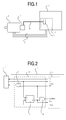
- FIG. 1 schematically illustrates a configuration in which a motor speed is controlled using an inverter device equipped with an interface circuit according to the first embodiment of the present invention.
- an inverter system includes a motor 1 and an inverter device 3.
- the inverter device 3 is configured to be capable of transmitting and receiving data to and from a serial encoder that detects the rotational position and speed of the motor 1.
- the inverter device 3 includes a main circuit (not shown) and a control board 4.
- the control board 4 generates a control signal for driving elements on the main circuit in accordance with a detection signal from a serial encoder 2.
- An interface circuit 7 is mounted on the control board 4.
- the interface circuit 7 is connected through a signal line 5 to the serial encoder 7 and performs bidirectional serial communication of clock synchronization type with the serial encoder 2.
- the main circuit (not shown) of the inverter device 3 is connected through motor lines 6 to the motor 1, and supplies the motor 1 with a power source having a variable voltage and a variable frequency.
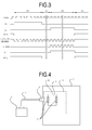
- FIG. 2 is a circuit diagram of the interface circuit according to the present embodiment.
- the interface circuit 7 includes a general-purpose CPU 8 and an additional circuit 20.
- the additional circuit 20 includes a flip-flop circuit 9, an AND circuit 10, and an OR circuit 11.
- FIG. 3 is a timing diagram illustrating an operation of the interface circuit according to the present embodiment.
- a period P1 is a period of time during which command transmission from the CPU 8 to the serial encoder 2 takes place.
- the CPU 8 In the period P1, the CPU 8 outputs a CLOCK signal to the serial encoder 2 and outputs eight bits of transmission data (TX) in synchronization with the CLOCK signal.
- the CLOCK signal is transmitted through the OR circuit 11.
- the CLOCK signal from the CPU 8 is connected to one input of the OR circuit 11, and the other input of the OR circuit 11 is connected to an OUT1 terminal of the CPU 8.
- the CPU 8 By driving a signal of the OUT1 terminal low simultaneously with the start of transmission of the transmission data (TX), the CPU 8 starts transmitting the CLOCK signal to the serial encoder 2.
- a period P2 is a period of time during which, after completion of command transmission from the CPU 8 to the serial encoder 2, the CPU 8 waits for a start bit of the reception data signal (RX).
- the reception data (RX) transmitted from the serial encoder 2 is connected to an RX terminal of the CPU 8 and also to an S terminal (set input terminal) of the flip-flop 9.
- An R terminal (reset input terminal) of the flip-flop 9 is connected to an OUT2 terminal of the CPU 8.
- the CPU 8 drives a signal of the OUT2 terminal from high to low, cancels the reset of the flip-flop circuit, and waits for a start bit of the reception data (RX).
- the reception of eight bits of data is repeated until the reception data (RX) goes high (until a start bit comes in). The data received before the start bit comes in is discarded.
- a period P3 is a period of time during which the reception data (RX) transmitted from the serial encoder 2 is received.
- the reception data (RX) is input to the S terminal of the flip-flop circuit 9 in the additional circuit 20.
- the flip-flop circuit 9 is triggered by the start bit to drive an output Q high.
- the flip-flop circuit 9 inputs, to an IN1 terminal of the CPU 8, a signal notifying that the reception data (RX) has been transmitted from the serial encoder 2.
- the AND circuit 10 inputs a CLOCK signal to a COUNTER terminal of the CPU 8.
- the CPU 8 has a counter.
- the CPU 8 detects the length of the reception data by counting the CLOCK signal.
- the reception data (RX) is a signal synchronized with the CLOCK signal. Therefore, by counting the CLOCK signal, the number of bits of the reception data (RX) can be counted and the reception data (RX) of a predetermined data length can be received. Note that the length of the reception data (RX) is set before communication takes place.
- a period P4 is a period of time during which the reception data (RX) is processed.
- the CPU 8 drives the OUT1 terminal high to stop transmission of the CLOCK signal to the serial encoder 2. At the same time, the CPU 8 drives the OUT2 terminal high to reset the flip-flop circuit 9, and disables the transmission of the reception data signal (RX) to the flip-flop circuit 9. Then, the CPU 8 processes the reception data (RX) input in the period P3.
- the data processing involves looking for a start bit while shifting the reception data (RX), and storing data following the start bit in a RAM (not shown).
- the data stored in the RAM is transmitted to the control board 4 as a signal which indicates a rotational position of the motor.
- the interface circuit 7 and the like according to the first embodiment of the present invention have been described.
- the interface circuit 7 is mainly composed of the general-purpose CPU 8 and the additional circuit 20 that detects a start bit (rising edge or starting point) of reception data from the serial encoder 2.
- the general-purpose CPU 8 can be used by using a simple additional circuit
- the interface circuit 7 serving as an interface to the serial encoder 2 can be realized which is low-cost and can be developed in a short period of time.
- the additional circuit 20 includes the flip-flop circuit 9 which is set by a start bit and is reset upon completion of counting a predetermined number of bits of reception data.
- the general-purpose CPU 8 can be used to receive a signal from the serial encoder 2. According to the present embodiment, it is thus possible to further reduce the cost of the interface circuit 7.
- the additional circuit 20 includes a gate circuit (e.g., OR circuit 11) and stops transmission of the CLOCK signal to the serial encoder in response to a clock stop signal from the CPU 8 upon completion of receiving reception data.
- a gate circuit e.g., OR circuit 11
- transmission of a signal from the serial encoder 20 can be stopped with a simple circuit. Therefore, according to the present embodiment, transmission and reception of data to and from the serial encoder can be controlled at a low cost.
- FIG. 4 illustrates a configuration of an inverter device according to the second embodiment of the present invention. Differences from the first embodiment will be mainly described here. A redundant description of the same configurations as those of the first embodiment will be omitted.
- the inverter device 3 includes an optional board 12 which includes the interface circuit 7.
- the optional board 12 is equipped with removable connectors 13 electrically connected to the control board 4. That is, unlike the interface circuit 7 of the first embodiment formed directly on the control board 4, the interface circuit 7 of the present embodiment is formed on a board removable from the control board 4. Therefore, the inverter device 3 of the present embodiment allows individual replacement of the interface circuit 7.
- the serial encoder 2 and the control board 4 are connected to each other by a signal cable 14 and a connector 15.
- the serial encoder 2 and the interface circuit 7 are connected to each other through the control board 4 by the connectors 12.
- the interface circuit 7 and the like according to the second embodiment of the present invention have been described.
- the interface circuit 7 is formed on the independent optional board 12 that can be selected depending on the type of the motor 1.
- the optional board 12 with the interface circuit 7 formed thereon is mounted on the control board 4 of the inverter device 3.
- the present embodiment allows the optional board 12 including the interface circuit 7 formed thereon to be individually replaced depending on the type of the motor 1. This can reduce the cost of, and the development time for, the inverter device 1.
- the interface circuit 7 includes the general-purpose CPU 8 equipped with a counter and the additional circuit 20, which includes the flip-flop circuit 9, the AND circuit 10, and the OR circuit 11.
- the additional circuit 20 is not limited to this example.
- the additional circuit 20 may be anything which can start counting the number of bits of reception data from a start bit, and can stop transmitting a clock to the serial encoder 2 upon completion of counting a predetermined number of bits of reception data.
Landscapes
- Engineering & Computer Science (AREA)
- Physics & Mathematics (AREA)
- General Physics & Mathematics (AREA)
- Theoretical Computer Science (AREA)
- Automation & Control Theory (AREA)
- General Engineering & Computer Science (AREA)
- Human Computer Interaction (AREA)
- Manufacturing & Machinery (AREA)
- Transmission And Conversion Of Sensor Element Output (AREA)
- Control Of Electric Motors In General (AREA)
- Inverter Devices (AREA)
Applications Claiming Priority (2)
| Application Number | Priority Date | Filing Date | Title |
|---|---|---|---|
| JP2009208420 | 2009-09-09 | ||
| PCT/JP2010/062684 WO2011030628A1 (ja) | 2009-09-09 | 2010-07-28 | インターフェース回路、インバータ装置、インバータシステム及び送受信方法 |
Publications (2)
| Publication Number | Publication Date |
|---|---|
| EP2477007A1 true EP2477007A1 (de) | 2012-07-18 |
| EP2477007A4 EP2477007A4 (de) | 2014-07-23 |
Family
ID=43732302
Family Applications (1)
| Application Number | Title | Priority Date | Filing Date |
|---|---|---|---|
| EP10815225.7A Withdrawn EP2477007A4 (de) | 2009-09-09 | 2010-07-28 | Schnittstellenschaltung, umrichtervorrichtung, umrichtersystem und sende-/empfangsverfahren |
Country Status (5)
| Country | Link |
|---|---|
| US (1) | US8918668B2 (de) |
| EP (1) | EP2477007A4 (de) |
| JP (1) | JP5177297B2 (de) |
| CN (1) | CN102575945B (de) |
| WO (1) | WO2011030628A1 (de) |
Cited By (1)
| Publication number | Priority date | Publication date | Assignee | Title |
|---|---|---|---|---|
| WO2016110393A1 (de) * | 2015-01-09 | 2016-07-14 | Schmidhauser Ag | Frequenzumrichter |
Families Citing this family (6)
| Publication number | Priority date | Publication date | Assignee | Title |
|---|---|---|---|---|
| CN104536330A (zh) * | 2014-11-13 | 2015-04-22 | 河北工业大学 | 用于ssi接口绝对值编码器数据通信的装置 |
| CN108141144B (zh) * | 2015-09-18 | 2020-10-23 | 株式会社安川电机 | 逆变器装置以及逆变器装置的制造方法 |
| CN108009107B (zh) * | 2017-07-20 | 2019-11-05 | 北京车和家信息技术有限责任公司 | 数据传输的方法、装置、存储介质及系统 |
| JP7255205B2 (ja) * | 2019-01-30 | 2023-04-11 | セイコーエプソン株式会社 | ロボットシステムおよびロボット制御装置 |
| CN111505934B (zh) * | 2020-04-30 | 2020-11-20 | 成都卡诺普自动化控制技术有限公司 | 基于biss编码器提高伺服驱动器采集速度和精度的方法 |
| JP7670575B2 (ja) * | 2021-08-03 | 2025-04-30 | 株式会社日立産機システム | サーボシステムおよびサーボシステムの制御方法 |
Family Cites Families (12)
| Publication number | Priority date | Publication date | Assignee | Title |
|---|---|---|---|---|
| JPH0755037B2 (ja) * | 1988-05-13 | 1995-06-07 | 株式会社日立製作所 | 永久磁石式同期電動機 |
| US5404459A (en) * | 1992-07-21 | 1995-04-04 | Advanced Micro Devices | Serial interface module and method in which the clock is only activated to send a predetermined number of data bits |
| US5495358A (en) * | 1992-11-23 | 1996-02-27 | Hewlett-Packard Company | Optical transceiver with improved range and data communication rate |
| JP2810617B2 (ja) * | 1993-06-23 | 1998-10-15 | 株式会社三協精機製作所 | 多重シリアル信号の伝送方法 |
| DE4342377B4 (de) | 1993-12-13 | 2010-08-12 | Dr. Johannes Heidenhain Gmbh | Anordnung und Verfahren zur seriellen Datenübertragung einer Positionsmeßeinrichtung |
| JPH0854254A (ja) * | 1994-08-15 | 1996-02-27 | Sankyo Seiki Mfg Co Ltd | アブソリュートエンコーダ |
| CN1037418C (zh) * | 1994-12-03 | 1998-02-18 | 李士华 | 程控变频定尺飞锯 |
| JPH08202469A (ja) * | 1995-01-30 | 1996-08-09 | Fujitsu Ltd | ユニバーサル非同期送受信回路を備えたマイクロ・コントローラユニット |
| WO1997036245A1 (en) * | 1996-03-25 | 1997-10-02 | Advanced Micro Devices, Inc. | Serial interface module and method |
| JP4212372B2 (ja) | 2003-01-29 | 2009-01-21 | 株式会社ハーモニック・ドライブ・システムズ | エンコーダ信号処理装置およびサーボドライバ |
| CN100451881C (zh) * | 2006-12-08 | 2009-01-14 | 清华大学 | 双电机冗余控制系统 |
| CN101369148B (zh) * | 2008-09-28 | 2010-09-29 | 西北工业大学 | 基于dsp的多轴交流电机同步伺服控制装置及其方法 |
-
2010
- 2010-07-28 JP JP2011530782A patent/JP5177297B2/ja not_active Expired - Fee Related
- 2010-07-28 WO PCT/JP2010/062684 patent/WO2011030628A1/ja not_active Ceased
- 2010-07-28 EP EP10815225.7A patent/EP2477007A4/de not_active Withdrawn
- 2010-07-28 CN CN201080038978.7A patent/CN102575945B/zh active Active
-
2012
- 2012-03-05 US US13/411,644 patent/US8918668B2/en not_active Expired - Fee Related
Cited By (2)
| Publication number | Priority date | Publication date | Assignee | Title |
|---|---|---|---|---|
| WO2016110393A1 (de) * | 2015-01-09 | 2016-07-14 | Schmidhauser Ag | Frequenzumrichter |
| US10346264B2 (en) | 2015-01-09 | 2019-07-09 | Schmidhauser Ag | Frequency converter |
Also Published As
| Publication number | Publication date |
|---|---|
| US20120166857A1 (en) | 2012-06-28 |
| US8918668B2 (en) | 2014-12-23 |
| EP2477007A4 (de) | 2014-07-23 |
| WO2011030628A1 (ja) | 2011-03-17 |
| JPWO2011030628A1 (ja) | 2013-02-04 |
| CN102575945B (zh) | 2015-07-01 |
| JP5177297B2 (ja) | 2013-04-03 |
| CN102575945A (zh) | 2012-07-11 |
Similar Documents
| Publication | Publication Date | Title |
|---|---|---|
| US8918668B2 (en) | Interface circuit, inverter device, inverter system, and transmitting and receiving method | |
| EP3187097A1 (de) | Kommunikationssystem | |
| EP2823404B1 (de) | Kollisionsdetektion in eia-485 bus-systemen | |
| US8948209B2 (en) | Transmission over an 12C bus | |
| EP2597540B1 (de) | Eingangsschaltung in einem Hochgeschwindigkeitszählermodul in einer Stromleitungskommunikation | |
| EP4377808B1 (de) | Fehler- und statusindikator mit niedriger latenz in der seriellen kommunikation | |
| US7986119B2 (en) | Motor control system | |
| CN107533533B (zh) | 集成电路之间的通信 | |
| CN113836075B (zh) | 一种基于fpga平台的spi接口信号消除毛刺的方法 | |
| EP4383557A1 (de) | Servosystem und steuerungsverfahren für das servosystem | |
| US20070061496A1 (en) | Electronic apparatus provided with electronic devices for serial communication and serial communication method | |
| KR101366034B1 (ko) | 터치센서 ic | |
| CN109768738A (zh) | 电动机控制装置、控制系统以及电动机控制方法 | |
| WO2016038685A1 (ja) | 多重通信装置 | |
| EP4213031B1 (de) | Verfahren und vorrichtung zur überwachung einer synchronen seriellen master/slave-verbindung unter verwendung einer asynchronen schnittstelle | |
| CN111159079A (zh) | 用于伺服驱动器识别编码器的转接口、识别方法及装置 | |
| EP4242860B1 (de) | Vorrichtung zur dekodierung der datenübertragung unter universeller serieller busnorm | |
| KR20140030159A (ko) | 디지털 인터페이스를 구비한 제어 장치 및 제어 장치용 마이크로 컨트롤러 | |
| US9350407B1 (en) | Interface chip and control method therefor | |
| CN118575441A (zh) | 半导体装置和电子设备 | |
| JP2007146696A (ja) | 電子制御装置 | |
| CN112286854A (zh) | Uart接口和spi接口的复用系统、方法及存储介质 | |
| TW201008106A (en) | Motor control system | |
| Kubiak | Autonomous Golf Cart Firmware | |
| WO2017123219A1 (en) | Two-wire bus to communicate signals |
Legal Events
| Date | Code | Title | Description |
|---|---|---|---|
| PUAI | Public reference made under article 153(3) epc to a published international application that has entered the european phase |
Free format text: ORIGINAL CODE: 0009012 |
|
| 17P | Request for examination filed |
Effective date: 20120307 |
|
| AK | Designated contracting states |
Kind code of ref document: A1 Designated state(s): AL AT BE BG CH CY CZ DE DK EE ES FI FR GB GR HR HU IE IS IT LI LT LU LV MC MK MT NL NO PL PT RO SE SI SK SM TR |
|
| DAX | Request for extension of the european patent (deleted) | ||
| A4 | Supplementary search report drawn up and despatched |
Effective date: 20140623 |
|
| RIC1 | Information provided on ipc code assigned before grant |
Ipc: G05B 19/042 20060101ALI20140616BHEP Ipc: G05B 19/414 20060101ALI20140616BHEP Ipc: H02P 25/04 20060101ALI20140616BHEP Ipc: H02P 27/06 20060101ALI20140616BHEP Ipc: G01D 5/249 20060101AFI20140616BHEP Ipc: H02M 7/48 20070101ALI20140616BHEP |
|
| STAA | Information on the status of an ep patent application or granted ep patent |
Free format text: STATUS: THE APPLICATION HAS BEEN WITHDRAWN |
|
| 18W | Application withdrawn |
Effective date: 20160822 |