EP2477172A1 - Aktivmatrixsubstrat und aktivmatrix-anzeigevorrichtung - Google Patents
Aktivmatrixsubstrat und aktivmatrix-anzeigevorrichtung Download PDFInfo
- Publication number
- EP2477172A1 EP2477172A1 EP10815188A EP10815188A EP2477172A1 EP 2477172 A1 EP2477172 A1 EP 2477172A1 EP 10815188 A EP10815188 A EP 10815188A EP 10815188 A EP10815188 A EP 10815188A EP 2477172 A1 EP2477172 A1 EP 2477172A1
- Authority
- EP
- European Patent Office
- Prior art keywords
- wires
- stem
- wire
- electrode layer
- active matrix
- Prior art date
- Legal status (The legal status is an assumption and is not a legal conclusion. Google has not performed a legal analysis and makes no representation as to the accuracy of the status listed.)
- Withdrawn
Links
Images




Classifications
-
- H—ELECTRICITY
- H10—SEMICONDUCTOR DEVICES; ELECTRIC SOLID-STATE DEVICES NOT OTHERWISE PROVIDED FOR
- H10K—ORGANIC ELECTRIC SOLID-STATE DEVICES
- H10K59/00—Integrated devices, or assemblies of multiple devices, comprising at least one organic light-emitting element covered by group H10K50/00
- H10K59/10—OLED displays
- H10K59/12—Active-matrix OLED [AMOLED] displays
- H10K59/131—Interconnections, e.g. wiring lines or terminals
-
- G—PHYSICS
- G02—OPTICS
- G02F—OPTICAL DEVICES OR ARRANGEMENTS FOR THE CONTROL OF LIGHT BY MODIFICATION OF THE OPTICAL PROPERTIES OF THE MEDIA OF THE ELEMENTS INVOLVED THEREIN; NON-LINEAR OPTICS; FREQUENCY-CHANGING OF LIGHT; OPTICAL LOGIC ELEMENTS; OPTICAL ANALOGUE/DIGITAL CONVERTERS
- G02F1/00—Devices or arrangements for the control of the intensity, colour, phase, polarisation or direction of light arriving from an independent light source, e.g. switching, gating or modulating; Non-linear optics
- G02F1/01—Devices or arrangements for the control of the intensity, colour, phase, polarisation or direction of light arriving from an independent light source, e.g. switching, gating or modulating; Non-linear optics for the control of the intensity, phase, polarisation or colour
- G02F1/13—Devices or arrangements for the control of the intensity, colour, phase, polarisation or direction of light arriving from an independent light source, e.g. switching, gating or modulating; Non-linear optics for the control of the intensity, phase, polarisation or colour based on liquid crystals, e.g. single liquid crystal display cells
- G02F1/133—Constructional arrangements; Operation of liquid crystal cells; Circuit arrangements
- G02F1/1333—Constructional arrangements; Manufacturing methods
- G02F1/1345—Conductors connecting electrodes to cell terminals
- G02F1/13452—Conductors connecting driver circuitry and terminals of panels
-
- G—PHYSICS
- G02—OPTICS
- G02F—OPTICAL DEVICES OR ARRANGEMENTS FOR THE CONTROL OF LIGHT BY MODIFICATION OF THE OPTICAL PROPERTIES OF THE MEDIA OF THE ELEMENTS INVOLVED THEREIN; NON-LINEAR OPTICS; FREQUENCY-CHANGING OF LIGHT; OPTICAL LOGIC ELEMENTS; OPTICAL ANALOGUE/DIGITAL CONVERTERS
- G02F1/00—Devices or arrangements for the control of the intensity, colour, phase, polarisation or direction of light arriving from an independent light source, e.g. switching, gating or modulating; Non-linear optics
- G02F1/01—Devices or arrangements for the control of the intensity, colour, phase, polarisation or direction of light arriving from an independent light source, e.g. switching, gating or modulating; Non-linear optics for the control of the intensity, phase, polarisation or colour
- G02F1/13—Devices or arrangements for the control of the intensity, colour, phase, polarisation or direction of light arriving from an independent light source, e.g. switching, gating or modulating; Non-linear optics for the control of the intensity, phase, polarisation or colour based on liquid crystals, e.g. single liquid crystal display cells
- G02F1/133—Constructional arrangements; Operation of liquid crystal cells; Circuit arrangements
- G02F1/1333—Constructional arrangements; Manufacturing methods
- G02F1/1345—Conductors connecting electrodes to cell terminals
- G02F1/13458—Terminal pads
-
- H—ELECTRICITY
- H10—SEMICONDUCTOR DEVICES; ELECTRIC SOLID-STATE DEVICES NOT OTHERWISE PROVIDED FOR
- H10D—INORGANIC ELECTRIC SEMICONDUCTOR DEVICES
- H10D86/00—Integrated devices formed in or on insulating or conducting substrates, e.g. formed in silicon-on-insulator [SOI] substrates or on stainless steel or glass substrates
- H10D86/40—Integrated devices formed in or on insulating or conducting substrates, e.g. formed in silicon-on-insulator [SOI] substrates or on stainless steel or glass substrates characterised by multiple TFTs
- H10D86/441—Interconnections, e.g. scanning lines
-
- H—ELECTRICITY
- H10—SEMICONDUCTOR DEVICES; ELECTRIC SOLID-STATE DEVICES NOT OTHERWISE PROVIDED FOR
- H10D—INORGANIC ELECTRIC SEMICONDUCTOR DEVICES
- H10D86/00—Integrated devices formed in or on insulating or conducting substrates, e.g. formed in silicon-on-insulator [SOI] substrates or on stainless steel or glass substrates
- H10D86/40—Integrated devices formed in or on insulating or conducting substrates, e.g. formed in silicon-on-insulator [SOI] substrates or on stainless steel or glass substrates characterised by multiple TFTs
- H10D86/60—Integrated devices formed in or on insulating or conducting substrates, e.g. formed in silicon-on-insulator [SOI] substrates or on stainless steel or glass substrates characterised by multiple TFTs wherein the TFTs are in active matrices
-
- G—PHYSICS
- G02—OPTICS
- G02F—OPTICAL DEVICES OR ARRANGEMENTS FOR THE CONTROL OF LIGHT BY MODIFICATION OF THE OPTICAL PROPERTIES OF THE MEDIA OF THE ELEMENTS INVOLVED THEREIN; NON-LINEAR OPTICS; FREQUENCY-CHANGING OF LIGHT; OPTICAL LOGIC ELEMENTS; OPTICAL ANALOGUE/DIGITAL CONVERTERS
- G02F1/00—Devices or arrangements for the control of the intensity, colour, phase, polarisation or direction of light arriving from an independent light source, e.g. switching, gating or modulating; Non-linear optics
- G02F1/01—Devices or arrangements for the control of the intensity, colour, phase, polarisation or direction of light arriving from an independent light source, e.g. switching, gating or modulating; Non-linear optics for the control of the intensity, phase, polarisation or colour
- G02F1/13—Devices or arrangements for the control of the intensity, colour, phase, polarisation or direction of light arriving from an independent light source, e.g. switching, gating or modulating; Non-linear optics for the control of the intensity, phase, polarisation or colour based on liquid crystals, e.g. single liquid crystal display cells
- G02F1/133—Constructional arrangements; Operation of liquid crystal cells; Circuit arrangements
- G02F1/1333—Constructional arrangements; Manufacturing methods
- G02F1/1335—Structural association of cells with optical devices, e.g. polarisers or reflectors
- G02F1/133553—Reflecting elements
-
- G—PHYSICS
- G02—OPTICS
- G02F—OPTICAL DEVICES OR ARRANGEMENTS FOR THE CONTROL OF LIGHT BY MODIFICATION OF THE OPTICAL PROPERTIES OF THE MEDIA OF THE ELEMENTS INVOLVED THEREIN; NON-LINEAR OPTICS; FREQUENCY-CHANGING OF LIGHT; OPTICAL LOGIC ELEMENTS; OPTICAL ANALOGUE/DIGITAL CONVERTERS
- G02F1/00—Devices or arrangements for the control of the intensity, colour, phase, polarisation or direction of light arriving from an independent light source, e.g. switching, gating or modulating; Non-linear optics
- G02F1/01—Devices or arrangements for the control of the intensity, colour, phase, polarisation or direction of light arriving from an independent light source, e.g. switching, gating or modulating; Non-linear optics for the control of the intensity, phase, polarisation or colour
- G02F1/13—Devices or arrangements for the control of the intensity, colour, phase, polarisation or direction of light arriving from an independent light source, e.g. switching, gating or modulating; Non-linear optics for the control of the intensity, phase, polarisation or colour based on liquid crystals, e.g. single liquid crystal display cells
- G02F1/133—Constructional arrangements; Operation of liquid crystal cells; Circuit arrangements
- G02F1/1333—Constructional arrangements; Manufacturing methods
- G02F1/1345—Conductors connecting electrodes to cell terminals
- G02F1/13454—Drivers integrated on the active matrix substrate
-
- G—PHYSICS
- G02—OPTICS
- G02F—OPTICAL DEVICES OR ARRANGEMENTS FOR THE CONTROL OF LIGHT BY MODIFICATION OF THE OPTICAL PROPERTIES OF THE MEDIA OF THE ELEMENTS INVOLVED THEREIN; NON-LINEAR OPTICS; FREQUENCY-CHANGING OF LIGHT; OPTICAL LOGIC ELEMENTS; OPTICAL ANALOGUE/DIGITAL CONVERTERS
- G02F1/00—Devices or arrangements for the control of the intensity, colour, phase, polarisation or direction of light arriving from an independent light source, e.g. switching, gating or modulating; Non-linear optics
- G02F1/01—Devices or arrangements for the control of the intensity, colour, phase, polarisation or direction of light arriving from an independent light source, e.g. switching, gating or modulating; Non-linear optics for the control of the intensity, phase, polarisation or colour
- G02F1/13—Devices or arrangements for the control of the intensity, colour, phase, polarisation or direction of light arriving from an independent light source, e.g. switching, gating or modulating; Non-linear optics for the control of the intensity, phase, polarisation or colour based on liquid crystals, e.g. single liquid crystal display cells
- G02F1/133—Constructional arrangements; Operation of liquid crystal cells; Circuit arrangements
- G02F1/136—Liquid crystal cells structurally associated with a semi-conducting layer or substrate, e.g. cells forming part of an integrated circuit
- G02F1/1362—Active matrix addressed cells
- G02F1/136286—Wiring, e.g. gate line, drain line
- G02F1/13629—Multilayer wirings
Definitions
- the present invention relates to an active matrix substrate on which a driving circuit and its wires have been monolithically formed and an active matrix display device including such a substrate.
- CTRs cathode-ray tubes
- active matrix display devices as typified by liquid crystal display devices and organic EL display devices, in which active elements such as TFTs are used, and the active matrix display devices have been widely used in televisions, monitors, cellular phones, etc. by utilizing their features of energy saving, thinness, lightweight, etc.
- GDM gate driver monolithic
- Patent Literature 1 discloses a liquid crystal display device including: pixel transistors provided in a display region of the liquid crystal display device; and a gate drive circuit (gate driver), provided in an area around the display region, which includes transistors, the pixel transistors and the transistors being monolithically formed by using an identical amorphous silicon layer.
- gate driver gate drive circuit
- Fig. 10 is a plan view showing the gate drive circuit of the liquid crystal display device and a wiring region of the gate drive circuit.
- Fig. 10 in the right edge region of the drawing, i.e., in a region (not illustrated) adjacent to the display region of the liquid crystal display device, there are provided driving transistors for driving shift registers.
- driving transistors for driving shift registers.
- the left edge region of the drawing i.e., in a region farthest from the display region, there is provided a wiring region where there are provided a plurality of main wires 150 through which signals are applied to the shift registers.
- control transistors for the shift registers there are provided control transistors for the shift registers.
- branch wires 160 electrically connecting the main wires 150 and the driving transistors of the shift registers and branch wires 160 electrically connecting the main wires 150 and the control transistors of the shift register are formed by a different layer from the main wires 150.
- the main wires 150 are formed by the same layer as a pattern of gate wires and gate electrodes
- the branch wires 160 are formed by the same layer as a pattern of data wires and source electrodes.
- an electrical connection between the control transistors, an electrical connection between the driving transistors, and an electrical connection between the control transistors and the driving transistors are made by using the same layer as the main wires 150 or the same layer as the branch wires 160.
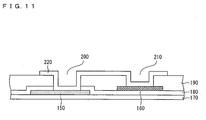
- Fig. 11 is a cross-sectional view, taken along the line G-H of Fig. 10 , which shows the appearance of an area of connection between a main wire 150 and a branch wire 160.
- the main wire 150 is provided on an insulating substrate 170
- the branch wire 160 is provided on a gate insulating film 180 formed in such a way as to cover the main wire 150 and the insulating substrate 170.
- passivation film 190 formed in such a way as to cover the branch wire 160 and the gate insulating film 180.
- first contact hole 200 which is a hole formed both in the gate insulating film 180 and the passivation film 190 so that part of the main wire 150 is exposed.
- second contact hole 210 which is a hole formed in the passivation film 190 so that part of the branch wire 160 is exposed.
- the main wire 150 and the branch wire 160 are electrically connected to each other through a connection conductor 220 formed both in the first contact hole 200 and the second contact hole 210, i.e., through the same layer as pixel electrodes electrically connected to drain electrodes of the pixel transistors provided in the display region of the liquid crystal display device.
- Patent Literature 1 states that the foregoing configuration allows the gate drive circuit and its wires to be formed at the same time as the display region by directly using the step of forming the display region of the liquid crystal display device, and as such, can integrate the gate drive circuit and its wires without adding a separate manufacturing step, thus achieving a reduction in manufacturing cost.
- the gate drive circuit and its wires are configured to include the main wires 150, the various transistors provided in the gate drive circuit, the branch wires 160 through which the main wires 150 and the gate or source electrodes of the various transistors are electrically connected, and the wires through which the gate or source electrodes of the various transistors are electrically connected.
- the gate drive circuit and its wires are generally provided in the right and left frame parts, which are nondisplay regions, of the display device. Therefore, the width of the frame parts is determined by the size and number of components that are provided in the gate drive circuit, the line widths of its wires, the intervals between its wires, etc.
- the width of such a frame part be narrow.
- the width of a frame part in a display device having a gate drive circuit monolithically formed by using amorphous silicon is prone to be great.
- the transistors including the amorphous silicon layer are low in electron mobility, they need to be formed to be large in size in order to satisfy the amount of current required of transistors for use in a gate drive circuit.
- main wires 150 through which clock signals and the like are supplied to the transistors of the gate drive circuit, need to be made lower in wiring resistance for the prevention of signal delays, and as such, are required to have wide line widths.
- Patent Literature 1 it is difficult to reduce the width of a region where its wires are formed, and the widths of the frame parts cannot be reduced.
- the present invention has been made in view of the foregoing problems, and it is an object of the present invention to provide an active matrix substrate on which a driving circuit and its wires have been monolithically formed, wherein the width of a frame part in which the driving circuit and its wires are formed can be reduced.
- an active matrix substrate of the present invention is an active matrix substrate including an insulating substrate, the insulating substrate having a display region including a plurality of pixel TFT elements and reflective pixel electrodes, the insulating substrate having a peripheral region, surrounding the display region, which includes a plurality of driving TFT elements for driving the pixel TFT elements, the peripheral region further including branch wires electrically connected to the driving TFT elements and first stem wires, electrically connected to the branch wires, through which external signals are inputted, the pixel TFT elements and the driving TFT elements including a gate electrode layer and a source and drain electrode layer, the reflective pixel electrodes being formed by a reflective pixel electrode layer that is different from the gate electrode layer and the source and drain electrode layers, the peripheral region having at least one second stem wire formed therein to extend along long sides of the first stem wires, the first stem wires, the at least one second stem wire, and the branch wires being formed by different layers selected from among the gate electrode layer, the source and drain electrode
- the stem wires, through which external signals and the like are supplied, are all formed by the same layer as the gate electrodes, the stem wires, through which different external signals are inputted, need to be placed at a distance from each other. This makes it difficult to reduce the intervals between the stem wires.
- the first stem wires, the at least one second stem wire, and the branch wires are formed by different layers selected from among the gate electrode layer, the source and drain electrode layer, and the reflective pixel electrode layer, respectively, and the at least one second stem wire is provided in such a way as to extend along a long side of its adjacent one of the first stem wires. Accordingly, the first and at least one second stem wires, through which different external signals are inputted, no longer need to be placed at a distance from each other. This makes it possible to increase the number of first and second stem wires per unit width.
- the foregoing configuration makes it possible to achieve an active matrix substrate on which a driving circuit and its wires have been monolithically formed, wherein the width of a frame part in which the driving circuit and its wires are formed can be reduced.
- the clause "the at least one second stem wire extends along a long side of its adjacent one of the first stem wires" not only means a case where the second stem wire and the first stem wire run parallel to each other but also includes, to the extent that the number of first and second stem wires per unit width can be increased, a case where the second stem wire and the first stem wire are slightly displaced from running parallel to each other.
- an active matrix display device of the present invention is configured to include such an active matrix substrate.
- the foregoing configuration makes it possible to achieve an active matrix display device that has a large display region.
- an active matrix substrate of the present invention is an active matrix substrate including an insulating substrate, the insulating substrate having a display region including a plurality of pixel TFT elements and reflective pixel electrodes, the insulating substrate having a peripheral region, surrounding the display region, which includes a plurality of driving TFT elements for driving the pixel TFT elements, the peripheral region further including branch wires electrically connected to the driving TFT elements and first stem wires, electrically connected to the branch wires, through which external signals are inputted, the pixel TFT elements and the driving TFT elements including a gate electrode layer and a source and drain electrode layer, the reflective pixel electrodes being formed by a reflective pixel electrode layer that is different from the gate electrode layer and the source and drain electrode layers, the peripheral region having at least one second stem wire formed therein to extend along long sides of the first stem wires, the first stem wires, the at least one second stem wire, and the branch wires being formed by different layers selected from among the gate electrode layer, the source and drain electrode layer, and the reflective pixel wires
- an active matrix display device of the present invention is configured to include such an active matrix substrate.
- This also brings about an effect of making it possible to achieve an active matrix display device that allows a reduction in the width of a frame part in which the driving circuit and its wires are formed and that has a large display region.
- a configuration of a TFT array substrate 1 serving as an active matrix substrate provided in a liquid crystal display device that is an example of an active matrix display device of the present invention is described below with reference to Fig. 5 .
- Fig. 5 schematically shows the configuration of the TFT array substrate 1.
- the TFT array substrate 1 includes a display region R1 and a peripheral region R2 located around the display region R1.
- a matrix of pixel TFT elements 2 Provided in the display region R1 is a matrix of pixel TFT elements 2, transparent pixel electrodes 3 electrically connected to the pixel TFT elements 2, and reflective pixel electrodes 4 (reflective pixel electrode layer).
- Each of the pixel TFT elements 2 includes: a gate electrode layer 6 and a Cs bus line 7, stacked on an insulating substrate 5, which form a gate bus line GL and a gate electrode; a gate insulating film 8 stacked on the insulating substrate 5, on the gate electrode layer 6, and on the Cs bus line 7; an amorphous silicon film 9, stacked on the gate insulating film 8, which serves as a semiconductor film; a source and drain electrode layer 10, stacked on the gate insulating film 8 and the amorphous silicon film 9, which forms a source electrode 10a, a drain electrode 10b, and a data bus line DL; a protective film 12, stacked on the gate insulating film 8, the amorphous silicon film9, and the source and drain electrode layer 10, in which a contact hole 11 is provided; an interlayer insulating film 13, stacked on the protective film 12, in which the contact hole 11 is provided; and a transparent pixel electrode 3, stacked on the source and drain electrode layer 10 and the interlayer insulating film 13, which has
- the interlayer insulating layer 13 has its upper surface formed in a roundly wavy shape 14.
- the transparent pixel electrode 3 On that part of the upper surface of the interlayer insulating film 13 which has been formed in the roundly wavy shape 14, the transparent pixel electrode 3 has a wavy shape, and the reflective pixel electrode 4, which is made of a conductor such as A1 or Ag having an optical reflectance, has a wavy shape, with the transparent pixel electrode 3 stacked on the interlayer insulating film 13 and the reflective pixel electrode 4 stacked on the transparent pixel electrode 3.
- the reflective pixel electrode 4 is electrically connected to the transparent pixel electrode 3.
- the reflective pixel electrode may be provided on the insulating layer without being electrically connected to the transparent pixel electrode.
- the TFT array substrate 1 is a transflective TFT array substrate including (i) transparent electrodes 3 that allow transmission of light from a backlight (not illustrated) provided on a side of the insulating substrate 5 opposite that side of the insulating substrate 5 on which the layers are provided and (ii) reflective pixel electrodes 4 that reflect outside light incident on a side opposite the side on which the backlight is provided
- the TFT array substrate 1 may be a reflective TFT array substrate constituted solely by reflective pixel electrodes 4 without being provided with transparent pixel electrodes 3.
- the pixel TFT elements 2 have their gate electrodes at the bottom. However, this does not imply any limitation. Alternatively, the pixel TFT elements 2 may of course have their gate electrodes at the top.
- a gate drive circuit 15 monolithically formed by using an amorphous silicon film 9 and a source drive circuit 16 formed by using a COG (chip on glass) technique.
- the gate drive circuit 15, electrically connected to the gate bus lines GL, and the source drive circuit 16, electrically connected to the data bus lines DL, are configured to control the pixel TFT elements 2 in accordance with external signals.
- gate drive circuit signal wires 17 composed of stem wires, such as clock signal lines and power supply voltage lines, and branch wires through which the stem wires and the gate drive circuit 15 are electrically connected.
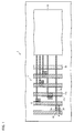
- Fig. 1 is a partly enlarged view showing a region in the TFT array substrate 1 where the gate drive circuit signal wires 17 are provided.
- the gate drive circuit signal wires 17 are constituted by (i) first stem wires 17a through which clock signals, power supply voltages, and the like are supplied to the gate drive circuit 15, (ii) branch wires 17b through which the first stem wires 17a and the gate drive circuit 15 are electrically connected, and (iii) second stem wires 17c electrically connected to the first stem wires 17a and formed in regions overlapping the first stem wires 17a when seen in a plan view.
- the gate drive circuit 15 comprises plural stages of gate drive circuits, one of which is shown in Fig. 1 .
- the single stage of gate drive circuit 15 is configured such that a plurality of branch wires 17b electrically connected to a plurality of different first stem wires 17a, respectively, are electrically connected thereto.
- the present embodiment uses a configuration in which five different types of signals (VSS/CK/CKB/VDD/VSS2) are sent to the single stage of gate drive circuit 15 through five different first stem wires 17a and branch wires 17b.
- the number is not particularly limited, and as such, can of course be changed as needed.
- the single state of gate drive circuit 15 comprises plural stages of gate drive circuits 15 coupled to each other.
- a stage of gate drive circuit 15 has its output terminal electrically connected to a gate bus line GL corresponding to an input terminal of a next stage, so that the plurality of gate bus lines GL are selected in sequence by output signals through such output terminals.
- this does not imply any limitation.
- each stage of gate drive circuit is provided, for example, with two output terminals one of which is electrically connected to the input terminal of the next stage and the other one of which is electrically connected to the gate bus line.
- Fig. 1 there may be provided a separate wire 18 between the gate drive circuit 15 and the five first stem wires 17a (five second stem wires 17c).
- the separate wire 18 may take the form of a wire for repairing breakage of a wire in a display region, an inspection signal wire, a wire for use in a counter (common) electrode, an auxiliary capacitor wire, etc.
- the gate drive circuit signal wires 17 are described further in detail with reference to Figs. 2 and 3 .
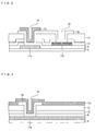
- Fig. 2 is a cross-sectional view, taken along the line A-B of Fig. 1 , which shows an area of connection between a first stem wire 17a and a branch wire 17b.
- the first stem wire 17a is formed by the same layer as the gate electrode layer 6 of each pixel TFT element 2 shown in Fig. 5
- the branch wire 17b is formed by the same layer as the source and drain electrode layer 10.
- the first stem wire 17a may be formed by the same layer as the source and drain electrode layer 10
- the branch wire 17b may be formed by the same layer as the gate electrode layer 6.
- the first stem wire 17a is provided on the insulating substrate 5, and the branch wire 17b is provided on the gate insulating film 8 formed in such a way as to cover the insulating substrate 5 and the first stem wire 17a.
- the protective film 12 and the interlayer insulating film 13 are provided in such a way as to cover the gate insulating film 8 and the branch wire 17b.
- first stem wire 17a there is a first contact hole 19 formed in the gate insulating film 8, the protective film 12, and the interlayer insulating film 13 so that part of the first stem wire 17a is exposed.
- branch wire 17b there is a second contact hole 20 formed in the protective film 12 and the interlayer insulating film 13 so that part of the branch wire 17b is exposed.
- the first and second stem wires 17a and 17c and the branch wire 17b are electrically connected through a connection conductor 3a formed by the same layer as the transparent electrodes 3 electrically connected to the pixel TFT elements 2 shown in Fig. 5 .
- the TFT array substrate 1 which is transflective, includes the transparent pixel electrodes 3, and in the present embodiment, the first and second stem wires 17a and 17c and the branch wire 17b are electrically connected by using the connection conductor 3a formed by the same layer as the transparent pixel electrodes 3.
- the first and second stem wires 17a and 17c and the branch wire 17b can also be electrically connected by using a connection conductor formed by the same layer as the reflective pixel electrodes 4.
- connection conductor be formed by using a conducting layer other than the transparent pixel electrodes 3 and the reflective pixel electrodes 4.
- connection conductor 3a formed by the same layer as the transparent pixel electrodes 3
- the second stem wire 17c is formed by the same layer as the reflective pixel electrodes 4.
- the first stem wire 17a is formed by the same layer as the gate electrode layer 6 of each pixel TFT element 2
- the branch wire 17b is formed by the same layer as the source and drain electrode layer 10
- the second stem wire 17c is formed by the same layer as the reflective pixel electrodes 4.
- the first stem wire 17a, the second stem wire 17c, and the branch wire 17b need only be formed by different layers selected from among the gate electrode layer 6, the source and drain electrode layer 10, and the same layer as the reflective pixel electrodes 4, respectively.
- the second stem wire 17c is formed by the same layer as the reflective pixel electrodes 4 and the first and second stem wires 17a and 17c and the branch wire 17b are electrically connected by using a connection conductor formed by the same layer as the reflective pixel electrodes 4, the first stem wire 17a and the branch wire 17b are electrically connected to each other through the second stem wire 17c.
- Fig. 3 is a cross-sectional view, taken along the line C-D of Fig. 1 , which shows an area of overlap between a first stem wire 17a and a second stem wire 17c.
- the second stem wire 17c extends along a long side of the first stem wire 17a (along a vertical direction in Fig. 1 ) in such a way as to be located above the first stem wire 17a when seen in a plan view, and is electrically connected to the first stem wire 17a through a connection conductor 3a.
- the main wires 150 through which external clock signals and the like are supplied, are formed by the same layer as the gate electrodes and need to be made lower in wiring resistance for the prevention of signal delays, and as such, have wide line widths. Therefore, it is difficult to reduce the width of a region in the driving circuit where its wires are formed, and the width of a frame part in which the driving circuit is formed cannot be reduced.
- the second stem wire 17a is formed by the same layer as the reflective pixel electrodes 4 and is electrically connected to the first stem wire 17a.
- a combined value of resistance per unit width of stem wires 17a and 17c with the first stem wire 17a electrically connected to the second stem wire 17c is smaller than a value of resistance per unit width of a first stem wire 17a not electrically connected to such a second stem wire 17c.
- the ratio of the value of resistance per unit width of a first stem wire 17a to the combined value of resistance per unit width of stem wires 17a and 17c with the first stem wire 17a electrically connected to the second stem wire 17c as can be obtained from a formula of parallel-connected resistors (1/R 1/R1 + 1/R2) is 3:2.
- the forgoing configuration in which the second stem wire 17c is electrically connected to the first stem wire 17a, can reduce the value of resistance per unit width to 2/3.
- each stem wire is constituted solely by a first stem wire 17a
- the line width W1 of the first stem wire 17a perpendicular to a long side of the first stem wire 17a is wide for lower wiring resistance.
- each stem wire is constituted by a first stem wire 17a and a second stem wire 17c
- the value of resistance per unit width can be reduced to 2/3. Therefore, to the extent that the value of resistance per unit width has been reduced, the line width W2 of each of the first and second stem wires 17a and 17b can be reduced.
- the ratio of the line width W1 to the line width W2 is 3:2.
- the second stem wires 17c are disposed above the first stem wires 17a in such a way as to overlap the first stem wires 17a when seen in a plan view.
- the first and second stem wires 17a and 17c are equal in wire width to each other along a direction perpendicular to their long sides and equal in length along their long sides.
- this does not imply any limitation.
- the second stem wires 17c overlap the first stem wires 17a when seen in a plan view, the second stem wires 17c do not need to be identical in shape to the first stem wires 17a.
- the first stem wires 17a i.e., the gate electrode layer 6 can be made, for example, of an aluminum alloy or the like.
- the first stem wires 17a, i.e., the gate electrode layer 6 may be made of an element selected from among Ta, W, Ti, Mo, Al, Cu, Cr, Nd, etc., an alloy material composed mainly of the element, or a compound material composed mainly of the element.
- the first stem wires 17a, i.e., the gate electrode layer 6 may be made by doping a semiconductor film as typified by polycrystalline silicon with an impurity such as boron.
- the branch wires 17b i.e., the source and drain electrode layer 10 can be made of an aluminum alloy, molybdenum, or a laminated film of them. However, this does not imply any limitation.
- the branch wires 17b, i.e., the source and drain electrode layer 10 may be formed as a laminated structure, as needed, made of an element selected from among Ta, W, Ti, Mo, Al, Cu, Cr, Nd, etc., an alloy material composed mainly of the element, or a compound material composed mainly of the element.
- the transparent pixel electrodes 3 and the connection conductors 3a which are the same layer as the transparent pixel electrodes 3, can be made by using a transparent conducting layer made of ITO (indium tin oxide), IZO (indium zinc oxide), or the like.
- the amorphous silicon film 9 is used as a semiconductor film to be provided in the pixel TFT element 2 and in the driving TFT elements to be described later.
- the semiconductor film may be made of amorphous germanium, amorphous silicon germanium, amorphous silicon carbide, or the like.
- the semiconductor film may be made of polycrystalline silicon, polycrystalline germanium, polycrystalline silicon germanium, polycrystalline silicon carbide, or the like.
- the driving TFT elements including the amorphous silicon layer as in the present embodiment are low in electron mobility, they need to be formed to be large in size in order to satisfy the amount of current required of TFT elements for use in a driving circuit.
- the gate drive circuit 15, which has the driving TFT elements including the amorphous silicon layer, is large in size; therefore, in order to reduce the width of a frame part in which the gate drive circuit 15 and the gate drive circuit signal wires 17 are formed, it is necessary to reduce the width of each of the gate drive circuit signal wires 17.
- the foregoing configuration makes it possible to realize a TFT array substrate 1 on which a gate drive circuit 15 having driving TFT elements including an amorphous silicon film 9, which is an amorphous semiconductor layer, and its gate drive circuit signal wires 17 have been monolithically formed, wherein the width of a frame part in which the gate drive circuit signal wires 17 are formed can be reduced.
- an inorganic film made of SiNx, SiOx, or the like can be used, for example. However, this does not imply any limitation.
- the interlayer insulating film 13 can be formed, for example, by an inorganic film made of SiNx or the like. However, this does not imply any limitation.
- the interlayer insulating film 13 may be formed by an inorganic film made of SiOx, SiON, or the like. Further, instead of such an inorganic film, an organic film made of transparent acrylic resin having photosensitivity can also be used. Alternatively, the interlayer insulating film 13 may be a laminated structure of an inorganic film and an organic film.
- the interlayer insulating film 13 in order for the interlayer insulating film 13 to have its upper surface formed partly in a roundly wavy shape 14, the interlayer insulating film 13 is formed by an organic film made of transparent acrylic resin having photosensitivity, and after patterning of a wavy shape, the wavy shape is subjected to melt flow to form a roundly wavy shape.
- the transparent pixel electrode 3 has a finely roundly wavy shape and the reflective pixel electrode 4 has a finely roundly wavy shape, with the reflective pixel electrode 4 stacked on the transparent pixel electrode 3.
- a TFT array substrate of the present embodiment on which a gate drive circuit 15 and its gate drive circuit signal wires 17 have been monolithically formed can be manufactured by directly using the process of manufacturing a transflective TFT array substrate including transparent pixel electrodes 3 and reflective pixel electrodes 4. Further, a TFT array substrate on which a gate drive circuit 15 and its gate drive circuit signal wires 17 have been monolithically formed by electrically connecting the first and second stem wires 17a and 17c and the branch wires 17b through connection conductors formed in the same layer as the reflective pixel electrodes 4 can be manufactured by directly using the process of manufacturing a conventional reflective TFT array including reflective pixel electrodes 4.
- a second embodiment of the present invention is described below with reference to Fig. 6 .
- the present embodiment differs from Embodiment 1 in that a second stem wires 17c is provided in such a way as to extend along a long side of its adjacent first stem wire 17a and is not electrically connected to the first stem wire 17a.
- the present embodiment is identical in configuration to Embodiment 1 described above.
- those members having the same functions as those shown in the drawings of Embodiment 1 are given the same reference numerals, and as such, are not described below.
- Fig. 6 is a partly enlarged view showing a region in a TFT array substrate 1 where gate drive circuit signal wires 17' are provided.
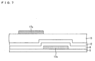
- Fig. 7 is a cross-sectional view taken along the line E-F in that part of the gate drive circuit signal wires 17' of Fig. 6 in which a first stem wire 17a and a second stem wire 17c are provided in such a way as to make contact with each other.
- the second stem wire 17c be provided in such a way as to extend along a long side of its adjacent first stem wire 17a.
- the second stem wire 17c is provided in such a way as to, when seen in a plan view, make contact with its adjacent first stem wire 17a on the right side in the drawing.
- the main wires 150 through which external signals and the like are supplied, are all formed by the same layer as the gate electrodes, the main wires 150, through which different external signals are inputted, need to be placed at a distance from each other. This makes it difficult to reduce the intervals between the main wires 150.
- the second stem wire 17c formed by the same layer as the reflective pixel electrodes 4 formed by a different layer from the first stem wires 17a formed by the same layer as the gate electrode layer 6 is provided in such a way as to, when seen in a plan view, make contact with its adjacent first stem wire 17a disposed therebelow.
- first and second stem wires 17a and 17c through which different external signals are inputted, no longer need to be placed at a distance from each other. This makes it possible to increase the number of first and second stem wires 17a and 17c per unit width.
- the second stem wire 17c is disposed above the first stem wire 17a, and the first stem wire 17a is disposed below the second stem wire 17c.
- the first stem wire 17a and the second stem wire 17c need only be formed by different layers from each other, and it does not particularly matter whether the second stem wire 17c is located above the first stem wire 17a or vice versa.
- the second stem wire 17c is placed between first stem wires 17a when seen in a plan view.
- this does not imply any limitation. It is only necessary that the second stem wire 17c be provided in such a way as to extend along a long side of its adjacent first stem wire 17a.
- the foregoing configuration makes it possible to achieve a TFT array substrate 1 on which a gate drive circuit 15 and its gate drive circuit signal wires 17' have been monolithically formed, wherein the width of a frame part in which the gate drive circuit signal wires 17' are formed can be reduced.
- a third embodiment of the present invention is described below with reference to Fig. 8 .
- the present embodiment differs from Embodiments 1 and 2 in that first stem wires 17a or one or more second stem wires 17c are electrically connected to driving TFT elements T1 and T2 provided in the gate drive circuit 15 through branch wires 17b' at least one of which is formed by the same layer as the reflective pixel electrodes 4.
- the present embodiment is identical in configuration to Embodiment 1 described above.
- those members having the same functions as those shown in the drawings of Embodiment 1 are given the same reference numerals, and as such, are not described below.
- a TFT array substrate 1 of the present embodiment is preferably configured such that first stem wires 17a or one or more second stem wires 17c are electrically connected to any of the gate, source, and drain electrodes of driving TFT elements T1 and T2 through branch wires 17b' at least one of which is formed by the same layer as the reflective pixel electrodes 4.
- each of the driving TFT elements T1and T2 provided in the gate drive circuit 15 includes a gate electrode formed by the gate electrode layer 6 and source and drain electrodes formed by the source and drain electrode layer 10.
- the gate drive circuit 15 has a third contact hole 21 formed therein so that part of the branch wire 17b is exposed and has a fourth contact hole 22 formed therein so that part of a wire L1 formed by the same layer as the gate electrode layer 6 electrically connected to the gate electrode of the driving TFT element T2 is exposed.
- the branch wire 17b and the wire L1 are electrically connected to each other through a connection conductor 3a formed by the same layer as the transparent pixel electrodes 3 electrically connected to the pixel TFT elements 2 shown in Fig. 5 .
- the method for electrical connection is not limited to this.
- the driving TFT element T1 includes a gate electrode formed by the gate electrode layer 6, the wire L1 formed by the same layer as the gate electrode layer 6 circumvents the driving TFT element T1, to which the wire L1 does not need to be electrically connected.
- (b) of Fig. 8 shows an example of a case where the gate electrode of a driving TFT element T2 provided in the gate drive circuit 15 and a branch wire 17b' electrically connected to a first stem wire 17a and formed by the same layer as the reflective pixel electrodes 4 are electrically connected to each other.
- the branch wire 17b' is formed by the same layer as the reflective pixel electrodes 4 formed by a different layer from the electrode layers (gate electrode layer 6, source and drain electrode layer 10) provided in the driving TFT elements T1 and T2 and from wires (wires formed by the same layers as the gate electrode layer 6 and the source and drain electrode layer 10; not illustrated) through which the gate, source, and drain electrodes of the driving TFT elements are electrically connected.
- the branch wire 17b' can avoid contact with the driving TFT element T1 and the wires without circumventing the driving TFT element T1, to which the branch wire 17b' does not need to be electrically connected, or the wires (not illustrated) through which the gate, source, and drain electrodes of the driving TFT elements are electrically connected. This makes it possible to reduce the amount of space in the gate drive circuit 15 that is occupied by the branch wire 17b' and the wire L1.
- the present embodiment is configured by forming a first contact hole 19 and a fourth contact hole 22 so that part of the first stem wire 17a and part of the wire L1 are exposed, then forming a connection conductor 3a on the contact holes 19 and 22, and further forming the branch wire 17b' on the connection conductor 3a.
- the method for electrical connection is not limited to this.
- the foregoing configuration makes it possible to achieve a TFT array substrate 1 on which a gate drive circuit 15 and its gate drive circuit signal wires 17 and 17' have been monolithically formed, wherein the width of a frame part in which the gate drive circuit 15 is formed can be reduced.
- a fourth embodiment of the present invention is described below with reference to Fig. 9 .
- the present embodiment differs from Embodiment 3 in that driving TFT elements T2 and T3 are electrically connected to each other through wires L3 at least one of which is formed by the same layer as the reflective pixel electrodes 4.
- the present embodiment is identical in configuration to Embodiment 3 described above.
- those members having the same functions as those shown in the drawings of Embodiment 3 are given the same reference numerals, and as such, are not described below.
- a TFT array substrate 1 of the present embodiment is preferably configured such that driving TFT elements T2 and T3 are electrically connected to each other through wires L3 at least one of which is formed by the same layer as the reflective pixel electrodes 4.
- the driving TFT T1 which does not need to be electrically connected, include a gate electrode formed by the gate electrode layer 6 and source and drain electrodes formed by the source and drain electrode layer 10, the wire L2, through which the source and drain electrodes of the driving TFT elements T2 and T3 are electrically connected, circumvents the driving TFT element T1, to which the wire L2 does not need to be electrically connected, as shown in (a) of Fig. 9 .
- FIG. 9 shows an example of a case where the source and drain electrodes of driving TFT elements T2 and T3 provided in the gate drive circuit 15 are electrically connected through a wire L3 formed by the same layer as the reflective pixel electrodes 4.
- the wire L3, through which the driving TFT elements T2 and T3 are electrically connected to each other, is formed by the same layer as the reflective pixel electrodes 4 formed by a different layer from the electrode layers (gate electrode layer 6, source and drain electrode layer 10) provided in the driving TFT elements T1, T2, and T3 and from wires (wires formed by the same layers as the gate electrode layer 6 and the source and drain electrode layer 10; not illustrated) through which the gate, source, and drain electrodes of the driving TFT elements are electrically connected.
- the wire L3 can avoid contact with the driving TFT element T1 and the wires without circumventing the driving TFT element T1, to which the wire L3 does not need to be electrically connected, or the wires (wires formed by the same layers as the gate electrode layer 6 and the source and drain electrode layer 10; not illustrated) through which the gate, source, and drain electrodes of driving TFT elements are electrically connected.
- This makes it possible to reduce the amount of space in the gate drive circuit 15 that is occupied by the wire L3, through which the driving TFT elements T2 and T3 are electrically connected to each other.
- the present embodiment is configured by forming a third contact hole 21 so that part of the wire L2 is exposed, then forming a connection conductor 3a on the third contact hole 21, and further forming the wire L3 on the connection conductor 3a.
- the method for electrical connection is not limited to this.
- the foregoing configuration makes it possible to achieve a TFT array substrate 1 on which a gate drive circuit 15 and its gate drive circuit signal wires 17 and 17' have been monolithically formed, wherein the width of a frame part in which the gate drive circuit 15 is formed can be reduced.
- a liquid crystal display device which is an example of an active matrix display device of the present invention, is configured to include such a TFT array substrate 1.
- the foregoing configuration makes it possible to achieve a liquid crystal display device that has a large display region.
- the liquid crystal display device for example includes a TFT array substrate 1 and a color filter substrate facing the TFT array substrate 1, with a liquid crystal layer sealed in a space between these substrates with a sealing agent.
- TFT array substrate 1 can of course be applied to other types of active matrix display device such as organic EL display devices.
- the active matrix substrate of the present invention is preferably configured such that the at least one second stem wire is provided in such a way that at least part of it overlaps its corresponding one of the first stem wires when seen in a plan view.
- the at least one second stem wires is provided in such a way that at least part of it overlaps its corresponding one of the first stem wires when seen in a plan view. This allows more efficient use of a wiring region where the first stem wires and the at least one second stem wire are formed, thus making it possible to achieve an active matrix substrate on which a driving circuit and its wires have been monolithically formed, wherein the width of a frame part in which the driving circuit and its wires are formed can be reduced.
- the active matrix substrate of the present invention is preferably configured such that the at least one second stem wire is electrically connected to its corresponding one of the first stem wires.
- the at least one second stem wire is electrically connected to its corresponding one of the first stem wires.
- a combined value of resistance per unit width of a first stem wire electrically connected to such a second stem wire is smaller than a value of resistance per unit width of a first stem wire not electrically connected to such a second stem wire.
- the ratio of the value of resistance per unit width of a first stem wire to the combined value of resistance per unit width of a first stem wire electrically connected to such a second stem wire as can be obtained from a formula of parallel-connected resistors is 3:2.
- the example in which the at least one second stem wire is electrically connected to its corresponding one of the first stem wires, can reduce the value of resistance per unit width to 2/3 as compared to the value of resistance of a first stem wire.
- the line width of each of the stem wires can be reduced.
- the active matrix substrate of the present invention is preferably configured such that: the branch wires are formed by a same layer as either the gate electrode layer or the source and drain electrode layer; the first stem wires are formed by a same layer as an electrode layer, selected from among the gate electrode layer or the source and drain electrode layer, which is different from an electrode layer forming the branch wires; and the at least one second stem wire is formed by a same layer as the reflective pixel electrode layer.
- the foregoing configuration makes it possible to achieve an active matrix substrate on which a driving circuit and its wires have been monolithically formed, wherein the width of a frame part in which the driving circuit and its wires are formed can be reduced.
- the active matrix substrate of the present invention is preferably configured such that: the display region further includes transparent electrodes electrically connected to the pixel TFT elements; and the first and at least one second stem wires and the branch wires are electrically connected to each other through connection conductors formed by a same layer as the transparent pixel electrodes.
- the first and at least one second stem wires and the branch wires in a transflective type of active matrix substrate including reflective pixel electrodes and transparent pixel electrodes in the display region can be electrically connected by directly using the step of forming the display region.
- the active matrix substrate of the present invention is preferably configured such that: the first stem wires and the at least one second stem wire are equal in wire width to each other along a direction perpendicular to their long sides and equal in length along their long sides; and the first stem wires and the at least one second stem wire have their main parts overlapping each other when seen in a plan view.
- the first stem wires and the at least one second stem wire are equal in wire width to each other. This allows more efficient use of a wiring region where the first stem wires and the at least one second stem wire are formed, thus making it possible to achieve an active matrix substrate on which a driving circuit and its wires have been monolithically formed, wherein the width of a frame part in which the driving circuit and its wires are formed can be reduced.
- the clause "the first stem wires and the at least one second stem wires have their main parts overlapping each other when seen in a plan view” means a configuration in which the first stem wires and the at least one second stem wires almost entirely overlap.
- the active matrix substrate of the present invention is preferably configured such that at least one of (a) a plurality of branch wires electrically connecting the first stem wires to each separate one of the driving TFT elements and (b) a branch wire(s) electrically connecting the at least one second stem wire to each separate one of the driving TFT elements is formed by the reflective pixel electrode layer.
- At least one of the branch wires is formed by the same layer as the reflective pixel elements formed by a different layer from the electrode layers (gate electrode layers, source and drain electrode layer) provided in the driving TFT elements and from the wires (gate electrode layer, source and drain electrode layer) through which the driving TFT elements are electrically connected to each other.
- the branch wire can avoid contact with the driving TFT element and the wires without circumventing the driving TFT element or the wires through the driving TFT elements are electrically connected to each other. This makes it possible to reduce the amount of space in the driving circuit that is occupied by the branch wire.
- the active matrix substrate of the present invention is preferably configured such that the driving TFT elements are electrically connected to each other through wires at least one of which is formed by the reflective pixel electrode layer.
- the wire, through which the driving TFT elements formed in the reflective pixel electrode layer are electrically connected to each other, is formed by a different layer from the electrode layers (gate electrode layer, source and drain electrode layer) provided in the driving TFT elements and from the wires (gate electrode layer, source and drain electrode layer) through which the driving TFT elements are electrically connected to each other.
- the wire, through which the driving TFT elements formed by the reflective pixel electrode layer are electrically connected to each other can avoid contact with the driving TFT element and the other wires without circumventing the driving TFT element or the wires (gate electrode layer 6, source and drain electrode layer) through which the driving TFT elements are electrically connected to each other.
- the active matrix substrate of the present invention is preferably configured such that the pixel TFT elements and the driving TFT elements include an amorphous semiconductor layer.
- the driving TFT elements including the amorphous silicon layer are low in electron mobility, they need to be formed to be large in size in order to satisfy the amount of current required of TFT elements for use in a driving circuit.
- the driving circuit which has the driving TFT elements including the amorphous silicon layer, is large in size; therefore, in order to reduce the width of a frame part in which the driving circuit and its wires are formed, it is necessary to reduce the width of a region where its wires are formed.
- the foregoing configuration makes it possible to achieve an active matrix substrate on which a driving circuit having driving TFT elements including an amorphous semiconductor layer and its wires have been monolithically formed, wherein the width of a frame part in which the driving circuit and its wires are formed can be reduced.
- the present invention can be applied to active matrix display devices such as liquid crystal display devices and organic EL display devices.
Landscapes
- Physics & Mathematics (AREA)
- Nonlinear Science (AREA)
- Mathematical Physics (AREA)
- Chemical & Material Sciences (AREA)
- Crystallography & Structural Chemistry (AREA)
- General Physics & Mathematics (AREA)
- Optics & Photonics (AREA)
- Engineering & Computer Science (AREA)
- Microelectronics & Electronic Packaging (AREA)
- Liquid Crystal (AREA)
- Devices For Indicating Variable Information By Combining Individual Elements (AREA)
Applications Claiming Priority (2)
| Application Number | Priority Date | Filing Date | Title |
|---|---|---|---|
| JP2009210387 | 2009-09-11 | ||
| PCT/JP2010/058666 WO2011030590A1 (ja) | 2009-09-11 | 2010-05-21 | アクティブマトリクス基板およびアクティブマトリクス型表示装置 |
Publications (2)
| Publication Number | Publication Date |
|---|---|
| EP2477172A1 true EP2477172A1 (de) | 2012-07-18 |
| EP2477172A4 EP2477172A4 (de) | 2016-03-23 |
Family
ID=43732267
Family Applications (1)
| Application Number | Title | Priority Date | Filing Date |
|---|---|---|---|
| EP10815188.7A Withdrawn EP2477172A4 (de) | 2009-09-11 | 2010-05-21 | Aktivmatrixsubstrat und aktivmatrix-anzeigevorrichtung |
Country Status (5)
| Country | Link |
|---|---|
| US (1) | US8586987B2 (de) |
| EP (1) | EP2477172A4 (de) |
| JP (1) | JP5236812B2 (de) |
| CN (1) | CN102483889B (de) |
| WO (1) | WO2011030590A1 (de) |
Cited By (1)
| Publication number | Priority date | Publication date | Assignee | Title |
|---|---|---|---|---|
| CN110658658A (zh) * | 2018-06-29 | 2020-01-07 | 夏普株式会社 | 图像显示装置 |
Families Citing this family (12)
| Publication number | Priority date | Publication date | Assignee | Title |
|---|---|---|---|---|
| CN103293727B (zh) * | 2012-06-29 | 2016-02-17 | 上海中航光电子有限公司 | 液晶显示装置的阵列基板 |
| KR20150081871A (ko) | 2014-01-07 | 2015-07-15 | 삼성디스플레이 주식회사 | 표시 장치 |
| US9589521B2 (en) * | 2014-11-20 | 2017-03-07 | Shenzhen China Star Optoelectronics Technology Co., Ltd. | Liquid crystal display apparatus having wire-on-array structure |
| CN109661701A (zh) * | 2016-09-01 | 2019-04-19 | 夏普株式会社 | 有源矩阵基板和显示装置 |
| CN109791745A (zh) * | 2016-09-27 | 2019-05-21 | 夏普株式会社 | 显示面板 |
| US10866471B2 (en) * | 2017-02-23 | 2020-12-15 | Sharp Kabushiki Kaisha | Drive circuit, matrix substrate, and display device |
| CN113325642B (zh) * | 2018-06-29 | 2022-12-30 | 上海中航光电子有限公司 | 一种阵列基板、显示面板及显示装置 |
| CN111091775B (zh) | 2020-03-22 | 2020-09-01 | 深圳市华星光电半导体显示技术有限公司 | 一种显示面板以及电子设备 |
| CN111679520A (zh) * | 2020-06-01 | 2020-09-18 | 深圳市华星光电半导体显示技术有限公司 | 显示面板及显示装置 |
| US11526232B2 (en) * | 2021-03-26 | 2022-12-13 | Wuhan China Star Optoelectronics Semiconductor Display Technology Co., Ltd. | Display module and display device |
| US11605359B2 (en) * | 2021-07-30 | 2023-03-14 | Sharp Display Technology Corporation | Display apparatus and display panel |
| CN115472630B (zh) * | 2022-07-21 | 2026-02-27 | 深圳莱宝高科技股份有限公司 | 多导电层走线结构、阵列基板及显示面板 |
Family Cites Families (23)
| Publication number | Priority date | Publication date | Assignee | Title |
|---|---|---|---|---|
| US5222082A (en) | 1991-02-28 | 1993-06-22 | Thomson Consumer Electronics, S.A. | Shift register useful as a select line scanner for liquid crystal display |
| JP3064596B2 (ja) * | 1991-11-29 | 2000-07-12 | セイコーエプソン株式会社 | 液晶パネルおよびその製造方法 |
| US5434899A (en) | 1994-08-12 | 1995-07-18 | Thomson Consumer Electronics, S.A. | Phase clocked shift register with cross connecting between stages |
| JP3647542B2 (ja) * | 1996-02-20 | 2005-05-11 | 株式会社半導体エネルギー研究所 | 液晶表示装置 |
| JP2776376B2 (ja) * | 1996-06-21 | 1998-07-16 | 日本電気株式会社 | アクティブマトリクス液晶表示パネル |
| JPH10198292A (ja) * | 1996-12-30 | 1998-07-31 | Semiconductor Energy Lab Co Ltd | 半導体装置およびその作製方法 |
| JP3856901B2 (ja) | 1997-04-15 | 2006-12-13 | 株式会社半導体エネルギー研究所 | 表示装置 |
| JP4036923B2 (ja) * | 1997-07-17 | 2008-01-23 | 株式会社半導体エネルギー研究所 | 表示装置およびその駆動回路 |
| JP3897873B2 (ja) * | 1997-09-11 | 2007-03-28 | 株式会社半導体エネルギー研究所 | 液晶表示装置の駆動回路 |
| US6066860A (en) * | 1997-12-25 | 2000-05-23 | Seiko Epson Corporation | Substrate for electro-optical apparatus, electro-optical apparatus, method for driving electro-optical apparatus, electronic device and projection display device |
| GB9825314D0 (en) * | 1998-11-20 | 1999-01-13 | Koninkl Philips Electronics Nv | Active matrix liquid crystal display devices |
| KR100685945B1 (ko) * | 2000-12-29 | 2007-02-23 | 엘지.필립스 엘시디 주식회사 | 액정표시장치 및 그 제조방법 |
| JP2003316284A (ja) * | 2002-04-24 | 2003-11-07 | Sanyo Electric Co Ltd | 表示装置 |
| KR100846464B1 (ko) * | 2002-05-28 | 2008-07-17 | 삼성전자주식회사 | 비정질실리콘 박막 트랜지스터-액정표시장치 및 그 제조방법 |
| JP3901127B2 (ja) | 2002-06-07 | 2007-04-04 | セイコーエプソン株式会社 | 電気光学装置及び電子機器 |
| JP4179199B2 (ja) * | 2003-06-02 | 2008-11-12 | セイコーエプソン株式会社 | 電気光学装置及びこれを備えた電子機器 |
| US7486269B2 (en) | 2003-07-09 | 2009-02-03 | Samsung Electronics Co., Ltd. | Shift register, scan driving circuit and display apparatus having the same |
| JP4058695B2 (ja) * | 2004-02-16 | 2008-03-12 | セイコーエプソン株式会社 | 電気光学装置及び電子機器 |
| KR101109963B1 (ko) * | 2005-02-18 | 2012-02-24 | 엘지디스플레이 주식회사 | 액정표시장치 및 그 제조방법 |
| KR20070003178A (ko) * | 2005-06-30 | 2007-01-05 | 엘지.필립스 엘시디 주식회사 | 액정표시소자 |
| KR101326594B1 (ko) * | 2006-12-15 | 2013-11-07 | 삼성디스플레이 주식회사 | 표시 장치 |
| JP2009015049A (ja) * | 2007-07-05 | 2009-01-22 | Toshiba Matsushita Display Technology Co Ltd | 液晶表示装置 |
| US8686422B2 (en) | 2009-07-16 | 2014-04-01 | Sharp Kabushiki Kaisha | Active matrix substrate and active matrix display device |
-
2010
- 2010-05-21 JP JP2011530770A patent/JP5236812B2/ja active Active
- 2010-05-21 WO PCT/JP2010/058666 patent/WO2011030590A1/ja not_active Ceased
- 2010-05-21 EP EP10815188.7A patent/EP2477172A4/de not_active Withdrawn
- 2010-05-21 CN CN201080039896.4A patent/CN102483889B/zh not_active Expired - Fee Related
- 2010-05-21 US US13/394,621 patent/US8586987B2/en not_active Expired - Fee Related
Cited By (2)
| Publication number | Priority date | Publication date | Assignee | Title |
|---|---|---|---|---|
| CN110658658A (zh) * | 2018-06-29 | 2020-01-07 | 夏普株式会社 | 图像显示装置 |
| CN110658658B (zh) * | 2018-06-29 | 2022-03-22 | 夏普株式会社 | 图像显示装置 |
Also Published As
| Publication number | Publication date |
|---|---|
| US8586987B2 (en) | 2013-11-19 |
| CN102483889B (zh) | 2014-09-03 |
| CN102483889A (zh) | 2012-05-30 |
| US20120168762A1 (en) | 2012-07-05 |
| EP2477172A4 (de) | 2016-03-23 |
| JP5236812B2 (ja) | 2013-07-17 |
| WO2011030590A1 (ja) | 2011-03-17 |
| JPWO2011030590A1 (ja) | 2013-02-04 |
Similar Documents
| Publication | Publication Date | Title |
|---|---|---|
| US8586987B2 (en) | Active matrix substrate and active matrix display device | |
| US10338443B2 (en) | Amorphous silicon thin film transistor-liquid crystal display device and method of manufacturing the same | |
| US10025149B2 (en) | Thin film transistor array panel and display device including the same | |
| JP5220918B2 (ja) | 表示装置 | |
| KR100848099B1 (ko) | 액정 표시 장치용 박막 트랜지스터 기판 | |
| EP2720082B1 (de) | Flüssigkristallanzeigevorrichtung mit integrierter Gatetreiberschaltung und reduzierter Rahmenbreite | |
| EP1245996A2 (de) | Anzeigegerät mit aktiver Matrix und Speicherkondensator für jeden Pixel | |
| US10254612B2 (en) | Display panel and method of fabricating the same | |
| US10495918B2 (en) | Display device comprising color filter | |
| KR20020081108A (ko) | 액정 표시 장치 | |
| KR101710575B1 (ko) | 액정표시장치용 어레이기판 및 그 제조방법 | |
| US20120218237A1 (en) | Display panel and display apparatus | |
| KR101687227B1 (ko) | 씨오지 타입 어레이 기판 | |
| KR102766820B1 (ko) | 베젤이 감소한 표시장치 | |
| CN118426228A (zh) | 显示装置 |
Legal Events
| Date | Code | Title | Description |
|---|---|---|---|
| PUAI | Public reference made under article 153(3) epc to a published international application that has entered the european phase |
Free format text: ORIGINAL CODE: 0009012 |
|
| 17P | Request for examination filed |
Effective date: 20120309 |
|
| AK | Designated contracting states |
Kind code of ref document: A1 Designated state(s): AL AT BE BG CH CY CZ DE DK EE ES FI FR GB GR HR HU IE IS IT LI LT LU LV MC MK MT NL NO PL PT RO SE SI SK SM TR |
|
| RIN1 | Information on inventor provided before grant (corrected) |
Inventor name: KIKUCHI, TETSUO Inventor name: SHIMADA, JUNYA Inventor name: YAMASAKI, CHIKAO Inventor name: TANAKA, SHINYA |
|
| DAX | Request for extension of the european patent (deleted) | ||
| RA4 | Supplementary search report drawn up and despatched (corrected) |
Effective date: 20160219 |
|
| RIC1 | Information provided on ipc code assigned before grant |
Ipc: H01L 27/32 20060101ALI20160215BHEP Ipc: H01L 51/50 20060101ALI20160215BHEP Ipc: G02F 1/1368 20060101ALI20160215BHEP Ipc: G09F 9/30 20060101AFI20160215BHEP Ipc: H01L 27/12 20060101ALI20160215BHEP |
|
| STAA | Information on the status of an ep patent application or granted ep patent |
Free format text: STATUS: THE APPLICATION HAS BEEN WITHDRAWN |
|
| 18W | Application withdrawn |
Effective date: 20160704 |