EP2477221B1 - Gestapelte Halbbrückenverpackung mit gängigem leitfähigem Leitungsrahmen - Google Patents
Gestapelte Halbbrückenverpackung mit gängigem leitfähigem Leitungsrahmen Download PDFInfo
- Publication number
- EP2477221B1 EP2477221B1 EP11191634.2A EP11191634A EP2477221B1 EP 2477221 B1 EP2477221 B1 EP 2477221B1 EP 11191634 A EP11191634 A EP 11191634A EP 2477221 B1 EP2477221 B1 EP 2477221B1
- Authority
- EP
- European Patent Office
- Prior art keywords
- sync
- control
- transistor
- bridge package
- leadframe
- Prior art date
- Legal status (The legal status is an assumption and is not a legal conclusion. Google has not performed a legal analysis and makes no representation as to the accuracy of the status listed.)
- Not-in-force
Links
Images


Classifications
-
- H—ELECTRICITY
- H10—SEMICONDUCTOR DEVICES; ELECTRIC SOLID-STATE DEVICES NOT OTHERWISE PROVIDED FOR
- H10W—GENERIC PACKAGES, INTERCONNECTIONS, CONNECTORS OR OTHER CONSTRUCTIONAL DETAILS OF DEVICES COVERED BY CLASS H10
- H10W90/00—Package configurations
-
- H—ELECTRICITY
- H10—SEMICONDUCTOR DEVICES; ELECTRIC SOLID-STATE DEVICES NOT OTHERWISE PROVIDED FOR
- H10W—GENERIC PACKAGES, INTERCONNECTIONS, CONNECTORS OR OTHER CONSTRUCTIONAL DETAILS OF DEVICES COVERED BY CLASS H10
- H10W70/00—Package substrates; Interposers; Redistribution layers [RDL]
- H10W70/01—Manufacture or treatment
- H10W70/05—Manufacture or treatment of insulating or insulated package substrates, or of interposers, or of redistribution layers
- H10W70/093—Connecting or disconnecting other interconnections thereto or therefrom, e.g. connecting bond wires or bumps
-
- H—ELECTRICITY
- H10—SEMICONDUCTOR DEVICES; ELECTRIC SOLID-STATE DEVICES NOT OTHERWISE PROVIDED FOR
- H10W—GENERIC PACKAGES, INTERCONNECTIONS, CONNECTORS OR OTHER CONSTRUCTIONAL DETAILS OF DEVICES COVERED BY CLASS H10
- H10W70/00—Package substrates; Interposers; Redistribution layers [RDL]
- H10W70/40—Leadframes
- H10W70/464—Additional interconnections in combination with leadframes
- H10W70/466—Tape carriers or flat leads
-
- H—ELECTRICITY
- H10—SEMICONDUCTOR DEVICES; ELECTRIC SOLID-STATE DEVICES NOT OTHERWISE PROVIDED FOR
- H10W—GENERIC PACKAGES, INTERCONNECTIONS, CONNECTORS OR OTHER CONSTRUCTIONAL DETAILS OF DEVICES COVERED BY CLASS H10
- H10W70/00—Package substrates; Interposers; Redistribution layers [RDL]
- H10W70/40—Leadframes
- H10W70/481—Leadframes for devices being provided for in groups H10D8/00 - H10D48/00
-
- H—ELECTRICITY
- H10—SEMICONDUCTOR DEVICES; ELECTRIC SOLID-STATE DEVICES NOT OTHERWISE PROVIDED FOR
- H10W—GENERIC PACKAGES, INTERCONNECTIONS, CONNECTORS OR OTHER CONSTRUCTIONAL DETAILS OF DEVICES COVERED BY CLASS H10
- H10W72/00—Interconnections or connectors in packages
- H10W72/60—Strap connectors, e.g. thick copper clips for grounding of power devices
-
- H—ELECTRICITY
- H10—SEMICONDUCTOR DEVICES; ELECTRIC SOLID-STATE DEVICES NOT OTHERWISE PROVIDED FOR
- H10W—GENERIC PACKAGES, INTERCONNECTIONS, CONNECTORS OR OTHER CONSTRUCTIONAL DETAILS OF DEVICES COVERED BY CLASS H10
- H10W90/00—Package configurations
- H10W90/811—Multiple chips on leadframes
-
- H—ELECTRICITY
- H10—SEMICONDUCTOR DEVICES; ELECTRIC SOLID-STATE DEVICES NOT OTHERWISE PROVIDED FOR
- H10W—GENERIC PACKAGES, INTERCONNECTIONS, CONNECTORS OR OTHER CONSTRUCTIONAL DETAILS OF DEVICES COVERED BY CLASS H10
- H10W72/00—Interconnections or connectors in packages
- H10W72/071—Connecting or disconnecting
- H10W72/073—Connecting or disconnecting of die-attach connectors
- H10W72/07331—Connecting techniques
- H10W72/07336—Soldering or alloying
-
- H—ELECTRICITY
- H10—SEMICONDUCTOR DEVICES; ELECTRIC SOLID-STATE DEVICES NOT OTHERWISE PROVIDED FOR
- H10W—GENERIC PACKAGES, INTERCONNECTIONS, CONNECTORS OR OTHER CONSTRUCTIONAL DETAILS OF DEVICES COVERED BY CLASS H10
- H10W72/00—Interconnections or connectors in packages
- H10W72/071—Connecting or disconnecting
- H10W72/076—Connecting or disconnecting of strap connectors
- H10W72/07631—Techniques
- H10W72/07636—Soldering or alloying
-
- H—ELECTRICITY
- H10—SEMICONDUCTOR DEVICES; ELECTRIC SOLID-STATE DEVICES NOT OTHERWISE PROVIDED FOR
- H10W—GENERIC PACKAGES, INTERCONNECTIONS, CONNECTORS OR OTHER CONSTRUCTIONAL DETAILS OF DEVICES COVERED BY CLASS H10
- H10W72/00—Interconnections or connectors in packages
- H10W72/071—Connecting or disconnecting
- H10W72/076—Connecting or disconnecting of strap connectors
- H10W72/07651—Connecting or disconnecting of strap connectors characterised by changes in properties of the strap connectors during connecting
- H10W72/07653—Connecting or disconnecting of strap connectors characterised by changes in properties of the strap connectors during connecting changes in shapes
-
- H—ELECTRICITY
- H10—SEMICONDUCTOR DEVICES; ELECTRIC SOLID-STATE DEVICES NOT OTHERWISE PROVIDED FOR
- H10W—GENERIC PACKAGES, INTERCONNECTIONS, CONNECTORS OR OTHER CONSTRUCTIONAL DETAILS OF DEVICES COVERED BY CLASS H10
- H10W72/00—Interconnections or connectors in packages
- H10W72/60—Strap connectors, e.g. thick copper clips for grounding of power devices
- H10W72/651—Materials of strap connectors
- H10W72/652—Materials of strap connectors comprising metals or metalloids, e.g. silver
-
- H—ELECTRICITY
- H10—SEMICONDUCTOR DEVICES; ELECTRIC SOLID-STATE DEVICES NOT OTHERWISE PROVIDED FOR
- H10W—GENERIC PACKAGES, INTERCONNECTIONS, CONNECTORS OR OTHER CONSTRUCTIONAL DETAILS OF DEVICES COVERED BY CLASS H10
- H10W72/00—Interconnections or connectors in packages
- H10W72/851—Dispositions of multiple connectors or interconnections
- H10W72/874—On different surfaces
- H10W72/886—Die-attach connectors and strap connectors
-
- H—ELECTRICITY
- H10—SEMICONDUCTOR DEVICES; ELECTRIC SOLID-STATE DEVICES NOT OTHERWISE PROVIDED FOR
- H10W—GENERIC PACKAGES, INTERCONNECTIONS, CONNECTORS OR OTHER CONSTRUCTIONAL DETAILS OF DEVICES COVERED BY CLASS H10
- H10W72/00—Interconnections or connectors in packages
- H10W72/90—Bond pads, in general
- H10W72/921—Structures or relative sizes of bond pads
- H10W72/926—Multiple bond pads having different sizes
-
- H—ELECTRICITY
- H10—SEMICONDUCTOR DEVICES; ELECTRIC SOLID-STATE DEVICES NOT OTHERWISE PROVIDED FOR
- H10W—GENERIC PACKAGES, INTERCONNECTIONS, CONNECTORS OR OTHER CONSTRUCTIONAL DETAILS OF DEVICES COVERED BY CLASS H10
- H10W74/00—Encapsulations, e.g. protective coatings
-
- H—ELECTRICITY
- H10—SEMICONDUCTOR DEVICES; ELECTRIC SOLID-STATE DEVICES NOT OTHERWISE PROVIDED FOR
- H10W—GENERIC PACKAGES, INTERCONNECTIONS, CONNECTORS OR OTHER CONSTRUCTIONAL DETAILS OF DEVICES COVERED BY CLASS H10
- H10W74/00—Encapsulations, e.g. protective coatings
- H10W74/10—Encapsulations, e.g. protective coatings characterised by their shape or disposition
- H10W74/111—Encapsulations, e.g. protective coatings characterised by their shape or disposition the semiconductor body being completely enclosed
-
- H—ELECTRICITY
- H10—SEMICONDUCTOR DEVICES; ELECTRIC SOLID-STATE DEVICES NOT OTHERWISE PROVIDED FOR
- H10W—GENERIC PACKAGES, INTERCONNECTIONS, CONNECTORS OR OTHER CONSTRUCTIONAL DETAILS OF DEVICES COVERED BY CLASS H10
- H10W90/00—Package configurations
- H10W90/701—Package configurations characterised by the relative positions of pads or connectors relative to package parts
- H10W90/731—Package configurations characterised by the relative positions of pads or connectors relative to package parts of die-attach connectors
- H10W90/736—Package configurations characterised by the relative positions of pads or connectors relative to package parts of die-attach connectors between a chip and a stacked lead frame, conducting package substrate or heat sink
-
- H—ELECTRICITY
- H10—SEMICONDUCTOR DEVICES; ELECTRIC SOLID-STATE DEVICES NOT OTHERWISE PROVIDED FOR
- H10W—GENERIC PACKAGES, INTERCONNECTIONS, CONNECTORS OR OTHER CONSTRUCTIONAL DETAILS OF DEVICES COVERED BY CLASS H10
- H10W90/00—Package configurations
- H10W90/701—Package configurations characterised by the relative positions of pads or connectors relative to package parts
- H10W90/761—Package configurations characterised by the relative positions of pads or connectors relative to package parts of strap connectors
- H10W90/766—Package configurations characterised by the relative positions of pads or connectors relative to package parts of strap connectors between a chip and a stacked lead frame, conducting package substrate or heat sink
Definitions
- the present invention relates generally to semiconductor devices. More particularly, the present invention relates to packaging of semiconductor devices.
- power converters such as buck converters
- buck converters commonly employ power switching circuits in which a high side power transistor and a low side power transistor are connected to form a half-bridge.
- One such power converter that is frequently employed is a synchronous buck converter, where the high side transistor is a control transistor and the low side transistor is a synchronous transistor.
- the control transistor and the synchronous transistor are typically formed on their respective separate dies, i.e. a control transistor die and a synchronous transistor die, that are connected in a package (i.e. co-packaged) to form the half-bridge.
- One approach to connecting the control transistor and the synchronous transistor in a package would be to arrange the control transistor and the synchronous transistor side by side on a substrate, such as a printed circuit board (PCB).
- PCB printed circuit board
- this arrangement would result in the package having a large footprint, as the package must be large enough to accommodate footprints of the control transistor and the synchronous transistor.
- conductive traces on the PCB could be used to connect the control transistor and the synchronous transistor so as to form the half-bridge package.
- the conductive traces would form long routing paths on the PCB, causing high parasitic inductance and resistance.
- this approach to packaging the control transistor and the synchronous transistor would result in a package having a large form factor where the package significantly degrades performance of the half-bridge.
- US 2006/169976 A1 discloses a stacked half bridge packet in accordance with the preamble of claim 1. The said document, however, is quiet regarding the relationship between the control source and the control gate on the one side and the control drain on the other side of the control transistor.
- a stacked half-bridge package with a common conductive leadframe substantially as shown in and/or described in connection with at least one of the figures, and as set forth more completely in the claims.
- the present application is directed to a stacked half-bridge package with a common conductive leadframe.
- the following description contains specific information pertaining to the implementation of the present invention.
- One skilled in the art will recognize that the present invention may be implemented in a manner different from that specifically discussed in the present application.
- some of the specific details of the invention are not discussed in order not to obscure the invention.
- the specific details not described in the present application are within the knowledge of a person of ordinary skill in the art.
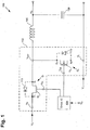
- FIG. 1 shows an exemplary circuit schematic of synchronous buck converter 100 including half-bridge 102, which is formed in a stacked half-bridge package according to an embodiment of the invention, and is thus also referred to as "stacked half-bridge package” 102 or “half-bridge package” 102 in the present application.
- Synchronous buck converter 100 also includes, driver integrated circuit (IC) 104, output inductor 106, and output capacitor 108.
- IC driver integrated circuit
- Half-bridge package 102 includes control transistor Q 1 and synchronous transistor Q 2 (also referred to as “sync transistor"), high voltage input terminal V H , low voltage input terminal V L , output terminal V out , control gate terminal V G1 , and sync gate terminal V G2 .
- high voltage input terminal V H receives high voltage input V HI , which can be, for example, a direct current (DC) voltage.
- Low voltage input terminal V L receives low voltage input V LI , which can be, for example, ground.
- control gate terminal V G1 receives a control gate signal from driver IC 104 for driving control transistor Q 1 .
- sync gate terminal V G2 receives a sync gate signal from driver IC 104 for driving sync transistor Q 2 .
- Driver IC 104 may drive control transistor Q 1 and sync transistor Q 2 utilizing any suitable method.
- driver IC 104 can vary a duty cycle of the sync and control gate signals responsive to a measurement of output voltage V O of synchronous buck converter 100 to maintain a desired output voltage V O , regardless of changes in high voltage input V HI . It will be appreciated that in other embodiments, output voltage V O is not measured in synchronous buck converter 100.
- Control transistor Q 1 includes control source S 1 , control drain D 1 , and control gate G 1 .
- Sync transistor Q 2 includes sync source S 2 , sync drain D 2 , and sync gate G 2 .
- control transistor Q 1 and sync transistor Q 2 can be any combination of an enhancement more transistor and a depletion mode transistor.
- control transistor Q 1 and sync transistor Q 2 are both depletion mode transistors.
- Control transistor Q 1 and sync transistor Q 2 can be P-channel or N-channel transistors.
- control transistor Q 1 and sync transistor Q 2 can be field-effect transistors (FETs).
- at least one of control transistor Q 1 and sync transistor Q 2 is a silicon FET.
- control transistor Q 1 and sync transistor Q 2 may also comprise a non-silicon FET or any other FET in general.
- at least one of control transistor Q 1 and sync transistor Q 2 is a metal-oxide-semiconductor field-effect transistor (MOSFET).
- MOSFET metal-oxide-semiconductor field-effect transistor
- At least one of control transistor Q 1 and sync transistor Q 2 can also be, as an example, a high electron mobility transistor (HEMT), such as a GaN HEMT.
- HEMT high electron mobility transistor
- Control transistor Q 1 has control drain D 1 for connection to high voltage input V H1 through high voltage input terminal V H of half-bridge package 102. Control transistor Q 1 also has control source S 1 coupled to output terminal V OUT of half-bridge package 102. Also, control transistor Q 1 has control gate G 1 coupled to control gate terminal V G1 of half-bridge package 102 for being driven by driver IC 104.
- Sync transistor Q 2 has sync drain D 2 for connection to output terminal V OUT of half-bridge package 102.
- Sync transistor Q 2 also has sync source S 2 coupled to low voltage input V LI through low voltage input terminal V L of half-bridge package 102.
- sync transistor Q 2 has sync gate G 2 coupled to sync gate terminal V G2 of half-bridge package 102 for being driven by driver IC 104.
- control transistor Q 1 and sync transistor Q 2 can be connected to a diode.
- Figure 1 shows optional diodes 110 and 112.
- diode 110 is coupled to control source Si and control drain D 1 , such that diode 110 is in parallel with control transistor Q 1 .
- diode 112 is coupled to sync source S 2 and sync drain D 2 , such that diode 112 is in parallel with control transistor Q 2 .
- at least one of diodes 110 and 112 can be connected with a reverse polarity to that shown in Figure 1 .
- diodes 110 and 112 can be internal to or external to control transistor Q 1 and sync transistor Q 2 .
- control transistor Q 1 and sync transistor Q 2 are MOSFETs and diodes 110 and 112 are respective body diodes of control transistor Q 1 and sync transistor Q 2 .
- Control transistor Q 1 and sync transistor Q 2 are commonly included on respective dies (i.e. a control transistor die and a synchronous transistor die).
- the respective dies may include other components, for example, diode 110 may be on the control transistor die and diode 112 may be on the synchronous transistor die. These other components may also be provided external to the respective dies and can be, for example, on a different die.
- Synchronous buck converter 100 illustrates one power converter, which can benefit from including stacked half-bridge package 102, in accordance with embodiments of the present invention.
- half-bridge package 102 is not limited to being included in a synchronous buck converter and can be included in other types of power converters.
- control transistor Q 1 and sync transistor Q 2 can be connected in a stacked half-bridge package, which includes stacked half-bridge package 102, while achieving a small footprint with low parasitic inductance and resistance.
- the stacked half-bridge package can have a small form factor where the stacked half-bridge package does not significantly degrade performance of half-bridge 102.
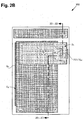
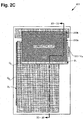
- Figures 2A-2C illustrate selective top views of stacked half-bridge package 202, corresponding to stacked half-bridge package 102 in Figure 1 , in accordance with one embodiment of the present invention.
- Various features of stacked half-bridge package 202 are not shown in Figures 2A-2C for clarity of description.
- Figure 2D illustrates a cross sectional view of a portion of stacked half-bridge package 202, according to one embodiment of the invention. The cross sectional view shown in Figure 2D corresponds to a cross section along line 2D-2D in Figures 2A-2C .
- FIG 2A shows control drain leadframe 220, control gate leadframe 222, common conductive leadframe 224, and sync transistor Q 2 of stacked half-bridge package 202.
- Sync transistor Q 2 in Figures 2A-2D corresponds to sync transistor Q 2 in Figure 1 .
- Common conductive lead frame 224 is over sync transistor Q 2 .
- dashed lines indicate portions of synch transistor Q 2 that would not otherwise be visible, as they are covered by common conductive leadframe 224.
- an outline of synch transistor Q 2 which can be a semiconductor die, is depicted using a dashed line.
- sync transistor Q 2 includes sync source S 2 and sync gate G 2 , which are depicted using dashed lines.
- Sync transistor Q 2 also includes sync drain D 2 , a portion of which is shown in Figure 2A , as it is not fully covered by common conductive leadframe 224 in the present embodiment.
- Sync source S 2 in stacked half-bridge package 202 corresponds to sync source S 2 in Figure 1
- sync gate G 2 in stacked half-bridge package 202 corresponds to sync gate G 2 in Figure 1
- sync drain D 2 in stacked half-bridge package 202 corresponds to sync drain D 2 in Figure 1
- sync transistor Q 2 has top and bottom surfaces, which are opposite one another. Sync drain D 2 is on the top surface and sync source S 2 and sync gate G 2 are on the bottom surface.
- sync drain D 2 is provided with a sync drain pad that substantially covers an entirety of the top surface of sync transistor Q 2 .
- sync source S 2 is provided with a plurality of sync source pads 228a, 228b, 228c, 228d, and 228e (also referred to collectively as "sync source pads 228").
- Sync source S 2 is exposed for electrical connection on a bottom surface of sync transistor Q 2 via sync source pads 228 (See Figure 2D ) and corresponds to low voltage input terminal V L in Figure 1 .
- Sync source pads 228 of sync source S 2 can include solderable front metal (SFM) that can be used for electrical connection to sync source S 2 .
- SFM solderable front metal
- sync gate G 2 is also exposed for electrical connection on a bottom surface of sync transistor Q 2 via a gate pad (See Figure 2D ) and corresponds to sync gate terminal V G2 in Figure 1 .
- Sync gate G 2 can also include SFM that can be used for electrical connection to sync source G 2 .
- sync drain D 2 , sync source S 2 , and sync gate G 2 are not provided as shown in stacked half-bridge package 202.
- sync drain D 2 , sync source S 2 , and sync gate G 2 can be provided on different surfaces of sync transistor Q 2 and can be provided using one or more pads arranged in any suitable manner.
- a single sync source pad can replace sync source pads 228.
- sync source S 2 and sync gate G 2 are not exposed for electrical connection as described above, and other layers or features can be connected to sync source S 2 and sync gate G 2 .
- Control drain leadframe 220, control gate leadframe 222, and common conductive leadframe 224 are electrically conductive and can comprise, for example, an easily solderable metal such as aluminum, and other solderable materials such as a metal alloy or a tri-metal.
- Common conductive leadframe 224 is over sync transistor Q 2 and is electrically and mechanically connected to sync drain D 2 .
- Figure 2B is similar to Figure 2A , with an addition of showing control transistor Q 1 of stacked half-bridge package 202 over common conductive leadframe 224 and sync transistor Q 2 .
- Control transistor Q 1 in stacked half-bridge package 202 corresponds to control transistor Q 1 in Figure 1 .
- dashed lines indicate portions of control transistor Q 1 that would not otherwise be visible. More particularly, control transistor Q 1 includes control source S 1 and control gate G 1 , which are depicted using dashed lines. Control transistor Q 1 also includes control drain D 1 , which is visible in Figure 2B .
- Control source S 1 in stacked half-bridge package 202 corresponds to control source S 1 in Figure 1
- control gate G 1 in stacked half-bridge package 202 corresponds to control gate G 1 in Figure 1
- control drain D 1 in stacked half-bridge package 202 corresponds to control drain D 1 in Figure 1
- control transistor Q 1 has top and bottom surfaces, which are opposite one another. Control drain D 1 is on the top surface and control source S 1 and control gate G 1 are on the bottom surface.
- control drain D 1 is provided with a control drain pad that substantially covers an entirety of the top surface of control transistor Q 1 .
- control source S 1 is provided with a plurality of control source pads 234a and 234b (also referred to as control source pads 234). In some embodiments, a single control source pad can replace control source pads 234.
- Control transistor Q 1 is over common conductive leadframe 224, which is electrically and mechanically connected to control source S 1 .
- control and sync transistors Q 1 and Q 2 are stacked on opposite sides of common conductive leadframe 224, with common conductive leadframe 224 electrically and mechanically coupling control source S 1 with sync drain D 2 .
- Common conductive leadframe 224 is thereby serving as output terminal V OUT of stacked half-bridge package 202, corresponding to output terminal V OUT in Figure 1 .
- a short current path is formed between control source S 1 and sync drain D 2 that has low parasitic inductance and resistance (See Figure 2D ).
- stacked half-bridge package 202 does not significantly degrade performance of half-bridge 102 in Figure 1 .
- stacked half-bridge package 202 has a small footprint that does not incorporate footprints of control transistor Q 1 and sync transistor Q 2 individually, thereby allowing for a small form factor.
- Control transistor Q 1 is also over control gate leadframe 222, which is electrically and mechanically connected to control gate G 2 .
- control gate leadframe 222 corresponds to control gate terminal V G1 in Figure 1 .
- Control gate leadframe 222 provides electrical and mechanical connection for control gate G 1 .
- Figure 2B shows a majority of control transistor Q 1 being over common conductive leadframe 224, with a portion of control transistor Q 1 overhanging common conductive leadframe 224 so as to accommodate connection between control gate G 1 and control gate leadframe 222.
- Figure 2C is similar to Figure 2B , with an addition of showing conductive clip 230 of stacked half-bridge package 202 over control transistor Q 1 , common conductive leadframe 224 and sync transistor Q 2 .
- Conductive clip 230 comprises conductive material, such as a metal or metal alloy. In one embodiment conductive clip 230 is a copper clip.
- Conductive clip 230 includes web portion 230a and leg portion 230b and provides connection between control drain D 1 and control drain leadframe 220.
- a dashed line indicates a boundary of web portion 230a and leg portion 230b.
- control drain leadframe 220 corresponds to high voltage input terminal V H in Figure 1 with leg portion 230b being over and electrically and mechanically connected to control drain leadframe 220 and web portion 230a being over and electrically and mechanically connected to control drain D 1 of control transistor Q 1 .
- Figure 2D illustrates a cross sectional view of a portion of stacked half-bridge package 202 corresponding to a cross section along line 2D-2D in Figures 2A-2C .
- Figure 2D shows hermetic sealant 236, which is optional as indicated by dashed lines.
- hermetic sealant 236 is a molding compound, which encapsulates stacked half-bridge package 202.
- Figure 2D shows hermetic sealant 236 leaves common conductive leadframe 224, sync gate G 2 , sync source S 2 , control gate leadframe 222, and control drain leadframe 220 exposed on bottomside 240b of stacked half-bridge package 202 and thus, available for electrical connection.
- FIG. 2D shows that in the present embodiment, common conductive leadframe 224 has web portion 224a and leg portion 224b.
- Leg portion 224b is of thickness 242, which is greater than that of sync transistor Q 2 and web portion 224a.
- control gate leadframe 222 is of thickness 242, which is greater than that of web portion 224a of common conductive leadframe 224 and is greater than that of sync transistor Q 1 .
- control drain leadframe 220 is of thickness 244, which is greater than that of web portion 224a of common conductive leadframe 224 and is greater than that of sync transistor Q 1 .
- respective bottom surfaces of sync transistor Q 1 , leg portion 224a of common conductive leadframe 224, conductive gate leadframe 222 and conductive drain leadframe 220 can thereby be substantially flush with one another, as shown in Figure 2D .
- stacked half-bridge package 202 can easily be mounted on and electrically connected to a substrate (not shown in Figures 2A-2D ).
- Figure 2D also shows that conductive clip 230 is connected to control drain D 2 at topside 240a of stacked half-bridge package 202.
- Leg portion 230b of conductive clip 230 is of thickness 244 that is greater than that of control transistor Q 1 and web portion 230a.
- respective top surfaces of control gate leadframe 222, control drain leadframe 220, and common conductive leadframe 224 can thereby be substantially flush with one another, as shown in Figure 2D .
- control gate leadframe 222, control drain leadframe 220, and common conductive leadframe 224 can be formed from a shared leadframe.
- common conductive leadframe 224 is an etched or half-etched leadframe that can be formed from the shared leadframe.
- Etching or half-etching common conductive leadframe 224 can be used to form leg portion 224b of common conductive leadframe 224.
- Figure 2D also illustrates that common conductive leadframe 224 electrically and mechanically couples the control source (source of control transistor Q1) with the sync drain (drain of sync transistor Q2) to form the output terminal of stacked half-bridge package 202.
- embodiments of the present invention can provide for a stacked half-bridge package including a control transistor and a sync transistor.
- the control transistor and the sync transistor can advantageously be connected in a half-bridge package with low parasitic inductance and resistance.
- the control transistor and the sync transistor can be connected with the stacked half-bridge package having a small footprint.
- the stacked half-bridge package can have a small form factor, where the stacked half-bridge package does not significantly degrade performance of the half-bridge.
Landscapes
- Dc-Dc Converters (AREA)
- Engineering & Computer Science (AREA)
- Manufacturing & Machinery (AREA)
- Electronic Switches (AREA)
- Lead Frames For Integrated Circuits (AREA)
Claims (14)
- Gestapeltes Halbbrückengehäuse (202), umfassend:einen Steuertransistor (Q1) mit einem Steuer-Drainanschluss (D1) zur Verbindung mit einem Hochspannungseingang (VH), einem Steuer-Sourceanschluss (S1), der mit einer Ausgangsklemme (VOUT) verbunden ist, und einem Steuer-Gateanschluss (G1), um durch eine integrierte Treiberschaltung angesteuert zu werden;einen Synchrontransistor (Q2) mit einem Synchron-Drainanschluss (D2) zur Verbindung mit der Ausgangsklemme (VOUT), einem Synchron-Sourceanschluss (S2), der mit einem Niederspannungseingang (VLI) verbunden ist, und einem Synchron-Gateanschluss (G2), um durch die integrierte Treiberschaltung angesteuert zu werden;wobei die Steuer- (Q1) und Synchrontransistoren (Q2) an entgegengesetzten Seiten eines gemeinsamen leitfähigen Trägerstreifens (224) gestapelt sind, wobei der gemeinsame leitfähige Trägerstreifen (224) den Steuer-Sourceanschluss (S1) elektrisch und mechanisch mit dem Synchron-Drainanschluss (D2) verbindet, wobei der gemeinsame leitfähige Trägerstreifen (224) dabei als Ausgangsklemme (VOUT) dient, dadurch gekennzeichnet, dass sich der Steuer-Sourceanschluss (S1) und der Steuer-Gateanschluss (G1) auf einer Oberfläche des Steuertransistors (Q1) befinden, die dem Steuer-Drainanschluss (D1) entgegengesetzt ist, wobei ein Steuer-Gateanschluss-Trägerstreifen (222) eine mechanische und elektrische Verbindung für den Steuer-Gateanschluss (G1) herstellt.
- Gestapeltes Halbbrückengehäuse (202) nach Anspruch 1, wobei der gemeinsame leitfähige Trägerstreifen (224) einen Stegabschnitt (224a) und einen Beinabschnitt (224b) umfasst.
- Gestapeltes Halbbrückengehäuse (202) nach Anspruch 1, wobei der gemeinsame leitfähige Trägerstreifen (224) einen Beinabschnitt (224b) umfasst, der eine größere Dicke als der Synchrontransistor (Q2) aufweist.
- Gestapeltes Halbbrückengehäuse (202) nach Anspruch 1, wobei jeweilige Bodenflächen des Synchrontransistors (Q2) und ein Beinabschnitt (224b) des gemeinsamen leitfähigen Trägerstreifens (224) bündig zueinander sind.
- Gestapeltes Halbbrückengehäuse (202) nach Anspruch 1, wobei ein leitfähiger Clip (230) eine Verbindung zwischen dem Steuer-Drainanschluss (D1) und einem Steuer-Drainanschluss-Trägerstreifen (220) herstellt.
- Gestapeltes Halbbrückengehäuse (202) nach Anspruch 1, umfassend einen leitfähigen Clip (230), der einen Stegabschnitt (230a) aufweist, der elektrisch und mechanisch mit dem Steuer-Drainanschluss (D1) verbunden ist, und der einen Beinabschnitt (230b) aufweist, der elektrisch und mechanisch mit einem Steuer-Drainanschluss-Trägerstreifen (220) verbunden ist.
- Gestapeltes Halbbrückengehäuse (202) nach Anspruch 1, wobei ein leitfähiger Clip (230) an einer Oberseite (240a) des gestapelten Halbbrückengehäuses (202) mit dem Steuer-Drainanschluss (D1) verbunden ist.
- Gestapeltes Halbbrückengehäuse (202) nach Anspruch 1, wobei der gemeinsame leitfähige Trägerstreifen (224) ein halbgeätzter Trägerstreifen ist.
- Gestapeltes Halbbrückengehäuse (202) nach Anspruch 1, wobei der Synchron-Sourceanschluss (S2) eine Vielzahl von Synchron-Sourceanschluss-Plättchen (228a - 228e) umfasst.
- Gestapeltes Halbbrückengehäuse (202) nach Anspruch 1, wobei der Synchron-Sourceanschluss (S2) ein lötfähiges Metall an der Vorderseite (SFM) (228) umfasst.
- Gestapeltes Halbbrückengehäuse (202) nach Anspruch 1, wobei der Synchron-Sourceanschluss (S2) für die elektrische Verbindung an einer Unterseite des Synchrontransistors (Q2) freiliegt.
- Gestapeltes Halbbrückengehäuse (202) nach Anspruch 1, wobei der Synchron-Gateanschluss (G2) für die elektrische Verbindung an einer Unterseite des Synchrontransistors (Q2) freiliegt.
- Gestapeltes Halbbrückengehäuse (202) nach Anspruch 1, wobei der Steuertransistor (Q1) Ober- und Unterseiten aufweist, wobei sich der Steuer-Drainanschluss (D1) an der Oberseite befindet und sich der Steuer-Sourceanschluss (S1) und der Steuer-Gateanschluss (G1) an der Unterseite befinden.
- Gestapeltes Halbbrückengehäuse (202) nach Anspruch 1, wobei der Synchrontransistor (Q2) Ober- und Unterseiten aufweist, wobei sich der Synchron-Drainanschluss (D2) an der Oberseite befindet und sich der Synchron-Sourceanschluss (S2) und der Synchron-Gateanschluss (G2) an der Unterseite befinden.
Applications Claiming Priority (2)
| Application Number | Priority Date | Filing Date | Title |
|---|---|---|---|
| US201161461110P | 2011-01-14 | 2011-01-14 | |
| US13/278,695 US8426952B2 (en) | 2011-01-14 | 2011-10-21 | Stacked half-bridge package with a common conductive leadframe |
Publications (3)
| Publication Number | Publication Date |
|---|---|
| EP2477221A2 EP2477221A2 (de) | 2012-07-18 |
| EP2477221A3 EP2477221A3 (de) | 2014-09-17 |
| EP2477221B1 true EP2477221B1 (de) | 2016-06-22 |
Family
ID=45047676
Family Applications (1)
| Application Number | Title | Priority Date | Filing Date |
|---|---|---|---|
| EP11191634.2A Not-in-force EP2477221B1 (de) | 2011-01-14 | 2011-12-01 | Gestapelte Halbbrückenverpackung mit gängigem leitfähigem Leitungsrahmen |
Country Status (2)
| Country | Link |
|---|---|
| US (3) | US8426952B2 (de) |
| EP (1) | EP2477221B1 (de) |
Families Citing this family (35)
| Publication number | Priority date | Publication date | Assignee | Title |
|---|---|---|---|---|
| US8637909B1 (en) * | 2010-08-11 | 2014-01-28 | Sarda Technologies, Inc. | Mixed mode dual switch |
| US8896034B1 (en) | 2010-08-11 | 2014-11-25 | Sarda Technologies, Inc. | Radio frequency and microwave devices and methods of use |
| US9236378B2 (en) | 2010-08-11 | 2016-01-12 | Sarda Technologies, Inc. | Integrated switch devices |
| TWI453831B (zh) | 2010-09-09 | 2014-09-21 | 台灣捷康綜合有限公司 | 半導體封裝結構及其製造方法 |
| US8749034B2 (en) * | 2011-01-03 | 2014-06-10 | International Rectifier Corporation | High power semiconductor package with conductive clip and flip chip driver IC with integrated control transistor |
| US8680627B2 (en) * | 2011-01-14 | 2014-03-25 | International Rectifier Corporation | Stacked half-bridge package with a common conductive clip |
| US8674497B2 (en) | 2011-01-14 | 2014-03-18 | International Business Machines Corporation | Stacked half-bridge package with a current carrying layer |
| US8426952B2 (en) | 2011-01-14 | 2013-04-23 | International Rectifier Corporation | Stacked half-bridge package with a common conductive leadframe |
| US8648643B2 (en) | 2012-02-24 | 2014-02-11 | Transphorm Inc. | Semiconductor power modules and devices |
| US9111776B2 (en) | 2012-10-18 | 2015-08-18 | International Rectifier Corporation | Power semiconductor package with non-contiguous, multi-section conductive carrier |
| US9111921B2 (en) * | 2012-10-18 | 2015-08-18 | International Rectifier Corporation | Semiconductor package with conductive carrier integrated heat spreader |
| US8860194B2 (en) * | 2012-11-01 | 2014-10-14 | International Rectifier Corporation | Buck converter power package |
| US9171837B2 (en) * | 2012-12-17 | 2015-10-27 | Nxp B.V. | Cascode circuit |
| US9379050B2 (en) * | 2013-02-28 | 2016-06-28 | Infineon Technologies Austria Ag | Electronic device |
| US9589929B2 (en) | 2013-03-14 | 2017-03-07 | Vishay-Siliconix | Method for fabricating stack die package |
| US9966330B2 (en) * | 2013-03-14 | 2018-05-08 | Vishay-Siliconix | Stack die package |
| CN105378917B (zh) | 2013-03-14 | 2018-09-25 | 维西埃-硅化物公司 | 堆叠芯片封装 |
| US9385070B2 (en) * | 2013-06-28 | 2016-07-05 | Delta Electronics, Inc. | Semiconductor component having a lateral semiconductor device and a vertical semiconductor device |
| US9536800B2 (en) | 2013-12-07 | 2017-01-03 | Fairchild Semiconductor Corporation | Packaged semiconductor devices and methods of manufacturing |
| US9620475B2 (en) | 2013-12-09 | 2017-04-11 | Infineon Technologies Americas Corp | Array based fabrication of power semiconductor package with integrated heat spreader |
| US9704787B2 (en) | 2014-10-16 | 2017-07-11 | Infineon Technologies Americas Corp. | Compact single-die power semiconductor package |
| US9570379B2 (en) | 2013-12-09 | 2017-02-14 | Infineon Technologies Americas Corp. | Power semiconductor package with integrated heat spreader and partially etched conductive carrier |
| US9653386B2 (en) * | 2014-10-16 | 2017-05-16 | Infineon Technologies Americas Corp. | Compact multi-die power semiconductor package |
| US9431327B2 (en) * | 2014-05-30 | 2016-08-30 | Delta Electronics, Inc. | Semiconductor device |
| DE102015104990B4 (de) * | 2015-03-31 | 2020-06-04 | Infineon Technologies Austria Ag | Verbindungshalbleitervorrichtung mit einem Abtastlead |
| US9774322B1 (en) | 2016-06-22 | 2017-09-26 | Sarda Technologies, Inc. | Gate driver for depletion-mode transistors |
| FR3054929A1 (fr) * | 2016-08-05 | 2018-02-09 | Commissariat Energie Atomique | Procede d'encapsulation d'un circuit integre avec une puce a transistor a heterojonction horizontal |
| US9923059B1 (en) | 2017-02-20 | 2018-03-20 | Silanna Asia Pte Ltd | Connection arrangements for integrated lateral diffusion field effect transistors |
| US10083897B2 (en) | 2017-02-20 | 2018-09-25 | Silanna Asia Pte Ltd | Connection arrangements for integrated lateral diffusion field effect transistors having a backside contact |
| WO2019082345A1 (ja) * | 2017-10-26 | 2019-05-02 | 新電元工業株式会社 | 半導体装置、及び、半導体装置の製造方法 |
| JP7059677B2 (ja) * | 2018-02-16 | 2022-04-26 | 富士電機株式会社 | 積層型集積回路 |
| US11158567B2 (en) * | 2019-08-09 | 2021-10-26 | Texas Instruments Incorporated | Package with stacked power stage and integrated control die |
| CN111463188B (zh) * | 2020-05-03 | 2025-02-18 | 矽力杰半导体技术(杭州)有限公司 | 应用于功率转换器的封装结构 |
| EP4123699A1 (de) * | 2021-07-22 | 2023-01-25 | Nexperia B.V. | Halbleiterbauelement und verfahren zur herstellung eines halbleiterbauelements |
| US12125771B2 (en) * | 2021-12-08 | 2024-10-22 | Nxp B.V. | Semiconductor package having lead frame with semiconductor die and component module mounted on opposite surfaces of the lead frame and methods of manufacture thereof |
Family Cites Families (29)
| Publication number | Priority date | Publication date | Assignee | Title |
|---|---|---|---|---|
| JP4426955B2 (ja) | 2004-11-30 | 2010-03-03 | 株式会社ルネサステクノロジ | 半導体装置 |
| JP2006216940A (ja) * | 2005-01-07 | 2006-08-17 | Toshiba Corp | 半導体装置 |
| JP2006324320A (ja) | 2005-05-17 | 2006-11-30 | Renesas Technology Corp | 半導体装置 |
| DE102005055761B4 (de) | 2005-11-21 | 2008-02-07 | Infineon Technologies Ag | Leistungshalbleiterbauelement mit Halbleiterchipstapel in Brückenschaltung und Verfahren zur Herstellung desselben |
| US7618896B2 (en) | 2006-04-24 | 2009-11-17 | Fairchild Semiconductor Corporation | Semiconductor die package including multiple dies and a common node structure |
| US7859089B2 (en) | 2006-05-04 | 2010-12-28 | International Rectifier Corporation | Copper straps |
| US7485954B2 (en) * | 2006-09-07 | 2009-02-03 | Alpha And Omega Semiconductor Limited | Stacked dual MOSFET package |
| US8674670B2 (en) | 2006-11-28 | 2014-03-18 | International Rectifier Corporation | DC/DC converter with depletion-mode III-nitride switches |
| US7902809B2 (en) | 2006-11-28 | 2011-03-08 | International Rectifier Corporation | DC/DC converter including a depletion mode power switch |
| KR101489325B1 (ko) | 2007-03-12 | 2015-02-06 | 페어차일드코리아반도체 주식회사 | 플립-칩 방식의 적층형 파워 모듈 및 그 파워 모듈의제조방법 |
| US7800208B2 (en) | 2007-10-26 | 2010-09-21 | Infineon Technologies Ag | Device with a plurality of semiconductor chips |
| KR101375831B1 (ko) | 2007-12-03 | 2014-04-02 | 삼성전자주식회사 | 산화물 반도체 박막 트랜지스터를 이용한 디스플레이 장치 |
| KR20090062612A (ko) | 2007-12-13 | 2009-06-17 | 페어차일드코리아반도체 주식회사 | 멀티 칩 패키지 |
| US7781872B2 (en) * | 2007-12-19 | 2010-08-24 | Fairchild Semiconductor Corporation | Package with multiple dies |
| US8642394B2 (en) | 2008-01-28 | 2014-02-04 | Infineon Technologies Ag | Method of manufacturing electronic device on leadframe |
| KR100958006B1 (ko) | 2008-06-18 | 2010-05-17 | 삼성모바일디스플레이주식회사 | 박막 트랜지스터, 그의 제조 방법 및 박막 트랜지스터를구비하는 평판 표시 장치 |
| US8062932B2 (en) | 2008-12-01 | 2011-11-22 | Alpha & Omega Semiconductor, Inc. | Compact semiconductor package with integrated bypass capacitor and method |
| US20100171543A1 (en) | 2009-01-08 | 2010-07-08 | Ciclon Semiconductor Device Corp. | Packaged power switching device |
| KR101097322B1 (ko) | 2009-12-15 | 2011-12-23 | 삼성모바일디스플레이주식회사 | 산화물 반도체 박막 트랜지스터, 그 제조방법 및 산화물 반도체 박막 트랜지스터를 구비한 유기전계 발광소자 |
| US8749034B2 (en) * | 2011-01-03 | 2014-06-10 | International Rectifier Corporation | High power semiconductor package with conductive clip and flip chip driver IC with integrated control transistor |
| US8426952B2 (en) * | 2011-01-14 | 2013-04-23 | International Rectifier Corporation | Stacked half-bridge package with a common conductive leadframe |
| DE102011008952A1 (de) * | 2011-01-19 | 2012-07-19 | Texas Instruments Deutschland Gmbh | Mehrchipmodul, Verfahren zum Betreiben desselben und DC/DC-Wandler |
| US8431979B2 (en) * | 2011-04-01 | 2013-04-30 | Texas Instruments Incorporated | Power converter having integrated capacitor |
| US8531016B2 (en) * | 2011-05-19 | 2013-09-10 | International Rectifier Corporation | Thermally enhanced semiconductor package with exposed parallel conductive clip |
| US8299588B1 (en) | 2011-07-07 | 2012-10-30 | Texas Instruments Incorporated | Structure and method for uniform current distribution in power supply module |
| US8946880B2 (en) * | 2012-03-23 | 2015-02-03 | Texas Instruments Incorporated | Packaged semiconductor device having multilevel leadframes configured as modules |
| US8860194B2 (en) * | 2012-11-01 | 2014-10-14 | International Rectifier Corporation | Buck converter power package |
| US9214415B2 (en) * | 2013-04-11 | 2015-12-15 | Texas Instruments Incorporated | Integrating multi-output power converters having vertically stacked semiconductor chips |
| US9171828B2 (en) * | 2014-02-05 | 2015-10-27 | Texas Instruments Incorporated | DC-DC converter having terminals of semiconductor chips directly attachable to circuit board |
-
2011
- 2011-10-21 US US13/278,695 patent/US8426952B2/en not_active Expired - Fee Related
- 2011-12-01 EP EP11191634.2A patent/EP2477221B1/de not_active Not-in-force
-
2013
- 2013-04-19 US US13/866,744 patent/US9349677B2/en active Active
-
2016
- 2016-05-17 US US15/157,298 patent/US9583477B2/en not_active Expired - Fee Related
Also Published As
| Publication number | Publication date |
|---|---|
| US20120181674A1 (en) | 2012-07-19 |
| EP2477221A3 (de) | 2014-09-17 |
| US9583477B2 (en) | 2017-02-28 |
| US9349677B2 (en) | 2016-05-24 |
| EP2477221A2 (de) | 2012-07-18 |
| US8426952B2 (en) | 2013-04-23 |
| US20130228794A1 (en) | 2013-09-05 |
| US20160260697A1 (en) | 2016-09-08 |
Similar Documents
| Publication | Publication Date | Title |
|---|---|---|
| EP2477221B1 (de) | Gestapelte Halbbrückenverpackung mit gängigem leitfähigem Leitungsrahmen | |
| EP2477220B1 (de) | Gestapelte Halbbrückenverpackung mit gängigem leitfähigem Clip | |
| EP2477222B1 (de) | Gestapelte Halbbrückenverpackung mit einer stromführenden Schicht | |
| US11996354B2 (en) | Semiconductor device | |
| CN101378053B (zh) | 高、低压侧n沟道金属氧化物半导体场效应晶体管组合封装 | |
| US8638577B2 (en) | Semiconductor device for DC-DC converter including high side and low side semiconductor switches | |
| US10727172B2 (en) | Semiconductor package | |
| US9653386B2 (en) | Compact multi-die power semiconductor package | |
| US7615854B2 (en) | Semiconductor package that includes stacked semiconductor die | |
| KR20110015043A (ko) | 반도체 장치 및 전원 시스템 | |
| US9831159B2 (en) | Semiconductor package with embedded output inductor | |
| US9780018B2 (en) | Power semiconductor package having reduced form factor and increased current carrying capability | |
| US20170117213A1 (en) | Semiconductor package with integrated die paddles for power stage | |
| US20130256905A1 (en) | Monolithic Power Converter Package with Through Substrate Vias | |
| JP2008270844A (ja) | 半導体装置 | |
| US9041175B2 (en) | Monolithic power converter package | |
| JP2011077550A (ja) | 半導体装置 |
Legal Events
| Date | Code | Title | Description |
|---|---|---|---|
| PUAI | Public reference made under article 153(3) epc to a published international application that has entered the european phase |
Free format text: ORIGINAL CODE: 0009012 |
|
| AK | Designated contracting states |
Kind code of ref document: A2 Designated state(s): AL AT BE BG CH CY CZ DE DK EE ES FI FR GB GR HR HU IE IS IT LI LT LU LV MC MK MT NL NO PL PT RO RS SE SI SK SM TR |
|
| AX | Request for extension of the european patent |
Extension state: BA ME |
|
| PUAL | Search report despatched |
Free format text: ORIGINAL CODE: 0009013 |
|
| AK | Designated contracting states |
Kind code of ref document: A3 Designated state(s): AL AT BE BG CH CY CZ DE DK EE ES FI FR GB GR HR HU IE IS IT LI LT LU LV MC MK MT NL NO PL PT RO RS SE SI SK SM TR |
|
| AX | Request for extension of the european patent |
Extension state: BA ME |
|
| RIC1 | Information provided on ipc code assigned before grant |
Ipc: H01L 23/495 20060101AFI20140811BHEP |
|
| 17P | Request for examination filed |
Effective date: 20150312 |
|
| RBV | Designated contracting states (corrected) |
Designated state(s): AL AT BE BG CH CY CZ DE DK EE ES FI FR GB GR HR HU IE IS IT LI LT LU LV MC MK MT NL NO PL PT RO RS SE SI SK SM TR |
|
| GRAP | Despatch of communication of intention to grant a patent |
Free format text: ORIGINAL CODE: EPIDOSNIGR1 |
|
| INTG | Intention to grant announced |
Effective date: 20160222 |
|
| GRAS | Grant fee paid |
Free format text: ORIGINAL CODE: EPIDOSNIGR3 |
|
| GRAA | (expected) grant |
Free format text: ORIGINAL CODE: 0009210 |
|
| AK | Designated contracting states |
Kind code of ref document: B1 Designated state(s): AL AT BE BG CH CY CZ DE DK EE ES FI FR GB GR HR HU IE IS IT LI LT LU LV MC MK MT NL NO PL PT RO RS SE SI SK SM TR |
|
| REG | Reference to a national code |
Ref country code: GB Ref legal event code: FG4D |
|
| REG | Reference to a national code |
Ref country code: CH Ref legal event code: EP |
|
| REG | Reference to a national code |
Ref country code: IE Ref legal event code: FG4D |
|
| REG | Reference to a national code |
Ref country code: AT Ref legal event code: REF Ref document number: 808109 Country of ref document: AT Kind code of ref document: T Effective date: 20160715 |
|
| REG | Reference to a national code |
Ref country code: DE Ref legal event code: R096 Ref document number: 602011027534 Country of ref document: DE |
|
| REG | Reference to a national code |
Ref country code: DE Ref legal event code: R081 Ref document number: 602011027534 Country of ref document: DE Owner name: INFINEON TECHNOLOGIES AMERICAS CORP. (N.D.GES., US Free format text: FORMER OWNER: INTERNATIONAL RECTIFIER CORPORATION, EL SEGUNDO, CALIF., US |
|
| REG | Reference to a national code |
Ref country code: LT Ref legal event code: MG4D |
|
| REG | Reference to a national code |
Ref country code: NL Ref legal event code: MP Effective date: 20160622 |
|
| PG25 | Lapsed in a contracting state [announced via postgrant information from national office to epo] |
Ref country code: LT Free format text: LAPSE BECAUSE OF FAILURE TO SUBMIT A TRANSLATION OF THE DESCRIPTION OR TO PAY THE FEE WITHIN THE PRESCRIBED TIME-LIMIT Effective date: 20160622 Ref country code: NO Free format text: LAPSE BECAUSE OF FAILURE TO SUBMIT A TRANSLATION OF THE DESCRIPTION OR TO PAY THE FEE WITHIN THE PRESCRIBED TIME-LIMIT Effective date: 20160922 Ref country code: FI Free format text: LAPSE BECAUSE OF FAILURE TO SUBMIT A TRANSLATION OF THE DESCRIPTION OR TO PAY THE FEE WITHIN THE PRESCRIBED TIME-LIMIT Effective date: 20160622 |
|
| REG | Reference to a national code |
Ref country code: AT Ref legal event code: MK05 Ref document number: 808109 Country of ref document: AT Kind code of ref document: T Effective date: 20160622 |
|
| PG25 | Lapsed in a contracting state [announced via postgrant information from national office to epo] |
Ref country code: NL Free format text: LAPSE BECAUSE OF FAILURE TO SUBMIT A TRANSLATION OF THE DESCRIPTION OR TO PAY THE FEE WITHIN THE PRESCRIBED TIME-LIMIT Effective date: 20160622 Ref country code: GR Free format text: LAPSE BECAUSE OF FAILURE TO SUBMIT A TRANSLATION OF THE DESCRIPTION OR TO PAY THE FEE WITHIN THE PRESCRIBED TIME-LIMIT Effective date: 20160923 Ref country code: LV Free format text: LAPSE BECAUSE OF FAILURE TO SUBMIT A TRANSLATION OF THE DESCRIPTION OR TO PAY THE FEE WITHIN THE PRESCRIBED TIME-LIMIT Effective date: 20160622 Ref country code: HR Free format text: LAPSE BECAUSE OF FAILURE TO SUBMIT A TRANSLATION OF THE DESCRIPTION OR TO PAY THE FEE WITHIN THE PRESCRIBED TIME-LIMIT Effective date: 20160622 Ref country code: RS Free format text: LAPSE BECAUSE OF FAILURE TO SUBMIT A TRANSLATION OF THE DESCRIPTION OR TO PAY THE FEE WITHIN THE PRESCRIBED TIME-LIMIT Effective date: 20160622 Ref country code: SE Free format text: LAPSE BECAUSE OF FAILURE TO SUBMIT A TRANSLATION OF THE DESCRIPTION OR TO PAY THE FEE WITHIN THE PRESCRIBED TIME-LIMIT Effective date: 20160622 |
|
| PG25 | Lapsed in a contracting state [announced via postgrant information from national office to epo] |
Ref country code: IT Free format text: LAPSE BECAUSE OF FAILURE TO SUBMIT A TRANSLATION OF THE DESCRIPTION OR TO PAY THE FEE WITHIN THE PRESCRIBED TIME-LIMIT Effective date: 20160622 Ref country code: IS Free format text: LAPSE BECAUSE OF FAILURE TO SUBMIT A TRANSLATION OF THE DESCRIPTION OR TO PAY THE FEE WITHIN THE PRESCRIBED TIME-LIMIT Effective date: 20161022 Ref country code: EE Free format text: LAPSE BECAUSE OF FAILURE TO SUBMIT A TRANSLATION OF THE DESCRIPTION OR TO PAY THE FEE WITHIN THE PRESCRIBED TIME-LIMIT Effective date: 20160622 Ref country code: RO Free format text: LAPSE BECAUSE OF FAILURE TO SUBMIT A TRANSLATION OF THE DESCRIPTION OR TO PAY THE FEE WITHIN THE PRESCRIBED TIME-LIMIT Effective date: 20160622 Ref country code: CZ Free format text: LAPSE BECAUSE OF FAILURE TO SUBMIT A TRANSLATION OF THE DESCRIPTION OR TO PAY THE FEE WITHIN THE PRESCRIBED TIME-LIMIT Effective date: 20160622 Ref country code: SK Free format text: LAPSE BECAUSE OF FAILURE TO SUBMIT A TRANSLATION OF THE DESCRIPTION OR TO PAY THE FEE WITHIN THE PRESCRIBED TIME-LIMIT Effective date: 20160622 |
|
| PG25 | Lapsed in a contracting state [announced via postgrant information from national office to epo] |
Ref country code: SM Free format text: LAPSE BECAUSE OF FAILURE TO SUBMIT A TRANSLATION OF THE DESCRIPTION OR TO PAY THE FEE WITHIN THE PRESCRIBED TIME-LIMIT Effective date: 20160622 Ref country code: AT Free format text: LAPSE BECAUSE OF FAILURE TO SUBMIT A TRANSLATION OF THE DESCRIPTION OR TO PAY THE FEE WITHIN THE PRESCRIBED TIME-LIMIT Effective date: 20160622 Ref country code: BE Free format text: LAPSE BECAUSE OF FAILURE TO SUBMIT A TRANSLATION OF THE DESCRIPTION OR TO PAY THE FEE WITHIN THE PRESCRIBED TIME-LIMIT Effective date: 20160622 Ref country code: PT Free format text: LAPSE BECAUSE OF FAILURE TO SUBMIT A TRANSLATION OF THE DESCRIPTION OR TO PAY THE FEE WITHIN THE PRESCRIBED TIME-LIMIT Effective date: 20161024 Ref country code: ES Free format text: LAPSE BECAUSE OF FAILURE TO SUBMIT A TRANSLATION OF THE DESCRIPTION OR TO PAY THE FEE WITHIN THE PRESCRIBED TIME-LIMIT Effective date: 20160622 Ref country code: PL Free format text: LAPSE BECAUSE OF FAILURE TO SUBMIT A TRANSLATION OF THE DESCRIPTION OR TO PAY THE FEE WITHIN THE PRESCRIBED TIME-LIMIT Effective date: 20160622 |
|
| REG | Reference to a national code |
Ref country code: DE Ref legal event code: R097 Ref document number: 602011027534 Country of ref document: DE |
|
| PLBE | No opposition filed within time limit |
Free format text: ORIGINAL CODE: 0009261 |
|
| STAA | Information on the status of an ep patent application or granted ep patent |
Free format text: STATUS: NO OPPOSITION FILED WITHIN TIME LIMIT |
|
| 26N | No opposition filed |
Effective date: 20170323 |
|
| PG25 | Lapsed in a contracting state [announced via postgrant information from national office to epo] |
Ref country code: DK Free format text: LAPSE BECAUSE OF FAILURE TO SUBMIT A TRANSLATION OF THE DESCRIPTION OR TO PAY THE FEE WITHIN THE PRESCRIBED TIME-LIMIT Effective date: 20160622 |
|
| REG | Reference to a national code |
Ref country code: CH Ref legal event code: PL |
|
| GBPC | Gb: european patent ceased through non-payment of renewal fee |
Effective date: 20161201 |
|
| PG25 | Lapsed in a contracting state [announced via postgrant information from national office to epo] |
Ref country code: SI Free format text: LAPSE BECAUSE OF FAILURE TO SUBMIT A TRANSLATION OF THE DESCRIPTION OR TO PAY THE FEE WITHIN THE PRESCRIBED TIME-LIMIT Effective date: 20160622 |
|
| PG25 | Lapsed in a contracting state [announced via postgrant information from national office to epo] |
Ref country code: MC Free format text: LAPSE BECAUSE OF FAILURE TO SUBMIT A TRANSLATION OF THE DESCRIPTION OR TO PAY THE FEE WITHIN THE PRESCRIBED TIME-LIMIT Effective date: 20160622 |
|
| REG | Reference to a national code |
Ref country code: FR Ref legal event code: ST Effective date: 20170831 |
|
| REG | Reference to a national code |
Ref country code: IE Ref legal event code: MM4A |
|
| PG25 | Lapsed in a contracting state [announced via postgrant information from national office to epo] |
Ref country code: LU Free format text: LAPSE BECAUSE OF NON-PAYMENT OF DUE FEES Effective date: 20161201 Ref country code: LI Free format text: LAPSE BECAUSE OF NON-PAYMENT OF DUE FEES Effective date: 20161231 Ref country code: CH Free format text: LAPSE BECAUSE OF NON-PAYMENT OF DUE FEES Effective date: 20161231 Ref country code: FR Free format text: LAPSE BECAUSE OF NON-PAYMENT OF DUE FEES Effective date: 20170102 |
|
| PG25 | Lapsed in a contracting state [announced via postgrant information from national office to epo] |
Ref country code: IE Free format text: LAPSE BECAUSE OF NON-PAYMENT OF DUE FEES Effective date: 20161201 Ref country code: GB Free format text: LAPSE BECAUSE OF NON-PAYMENT OF DUE FEES Effective date: 20161201 |
|
| PG25 | Lapsed in a contracting state [announced via postgrant information from national office to epo] |
Ref country code: CY Free format text: LAPSE BECAUSE OF FAILURE TO SUBMIT A TRANSLATION OF THE DESCRIPTION OR TO PAY THE FEE WITHIN THE PRESCRIBED TIME-LIMIT Effective date: 20160622 Ref country code: HU Free format text: LAPSE BECAUSE OF FAILURE TO SUBMIT A TRANSLATION OF THE DESCRIPTION OR TO PAY THE FEE WITHIN THE PRESCRIBED TIME-LIMIT; INVALID AB INITIO Effective date: 20111201 |
|
| PG25 | Lapsed in a contracting state [announced via postgrant information from national office to epo] |
Ref country code: MK Free format text: LAPSE BECAUSE OF FAILURE TO SUBMIT A TRANSLATION OF THE DESCRIPTION OR TO PAY THE FEE WITHIN THE PRESCRIBED TIME-LIMIT Effective date: 20160622 Ref country code: TR Free format text: LAPSE BECAUSE OF FAILURE TO SUBMIT A TRANSLATION OF THE DESCRIPTION OR TO PAY THE FEE WITHIN THE PRESCRIBED TIME-LIMIT Effective date: 20160622 |
|
| PG25 | Lapsed in a contracting state [announced via postgrant information from national office to epo] |
Ref country code: BG Free format text: LAPSE BECAUSE OF FAILURE TO SUBMIT A TRANSLATION OF THE DESCRIPTION OR TO PAY THE FEE WITHIN THE PRESCRIBED TIME-LIMIT Effective date: 20160622 |
|
| PG25 | Lapsed in a contracting state [announced via postgrant information from national office to epo] |
Ref country code: MT Free format text: LAPSE BECAUSE OF NON-PAYMENT OF DUE FEES Effective date: 20161201 |
|
| PG25 | Lapsed in a contracting state [announced via postgrant information from national office to epo] |
Ref country code: AL Free format text: LAPSE BECAUSE OF FAILURE TO SUBMIT A TRANSLATION OF THE DESCRIPTION OR TO PAY THE FEE WITHIN THE PRESCRIBED TIME-LIMIT Effective date: 20160622 |
|
| P01 | Opt-out of the competence of the unified patent court (upc) registered |
Effective date: 20230528 |
|
| PGFP | Annual fee paid to national office [announced via postgrant information from national office to epo] |
Ref country code: DE Payment date: 20240221 Year of fee payment: 13 |
|
| REG | Reference to a national code |
Ref country code: DE Ref legal event code: R119 Ref document number: 602011027534 Country of ref document: DE |
|
| PG25 | Lapsed in a contracting state [announced via postgrant information from national office to epo] |
Ref country code: DE Free format text: LAPSE BECAUSE OF NON-PAYMENT OF DUE FEES Effective date: 20250701 |