EP2479794A1 - Cellule solaire - Google Patents
Cellule solaire Download PDFInfo
- Publication number
- EP2479794A1 EP2479794A1 EP11006399A EP11006399A EP2479794A1 EP 2479794 A1 EP2479794 A1 EP 2479794A1 EP 11006399 A EP11006399 A EP 11006399A EP 11006399 A EP11006399 A EP 11006399A EP 2479794 A1 EP2479794 A1 EP 2479794A1
- Authority
- EP
- European Patent Office
- Prior art keywords
- layer
- substrate
- solar cell
- back surface
- protective layer
- Prior art date
- Legal status (The legal status is an assumption and is not a legal conclusion. Google has not performed a legal analysis and makes no representation as to the accuracy of the status listed.)
- Ceased
Links
Images


Classifications
-
- H—ELECTRICITY
- H10—SEMICONDUCTOR DEVICES; ELECTRIC SOLID-STATE DEVICES NOT OTHERWISE PROVIDED FOR
- H10F—INORGANIC SEMICONDUCTOR DEVICES SENSITIVE TO INFRARED RADIATION, LIGHT, ELECTROMAGNETIC RADIATION OF SHORTER WAVELENGTH OR CORPUSCULAR RADIATION
- H10F77/00—Constructional details of devices covered by this subclass
- H10F77/30—Coatings
- H10F77/306—Coatings for devices having potential barriers
- H10F77/311—Coatings for devices having potential barriers for photovoltaic cells
-
- H—ELECTRICITY
- H10—SEMICONDUCTOR DEVICES; ELECTRIC SOLID-STATE DEVICES NOT OTHERWISE PROVIDED FOR
- H10F—INORGANIC SEMICONDUCTOR DEVICES SENSITIVE TO INFRARED RADIATION, LIGHT, ELECTROMAGNETIC RADIATION OF SHORTER WAVELENGTH OR CORPUSCULAR RADIATION
- H10F10/00—Individual photovoltaic cells, e.g. solar cells
- H10F10/10—Individual photovoltaic cells, e.g. solar cells having potential barriers
- H10F10/14—Photovoltaic cells having only PN homojunction potential barriers
-
- H—ELECTRICITY
- H10—SEMICONDUCTOR DEVICES; ELECTRIC SOLID-STATE DEVICES NOT OTHERWISE PROVIDED FOR
- H10F—INORGANIC SEMICONDUCTOR DEVICES SENSITIVE TO INFRARED RADIATION, LIGHT, ELECTROMAGNETIC RADIATION OF SHORTER WAVELENGTH OR CORPUSCULAR RADIATION
- H10F10/00—Individual photovoltaic cells, e.g. solar cells
- H10F10/10—Individual photovoltaic cells, e.g. solar cells having potential barriers
- H10F10/14—Photovoltaic cells having only PN homojunction potential barriers
- H10F10/148—Double-emitter photovoltaic cells, e.g. bifacial photovoltaic cells
-
- H—ELECTRICITY
- H10—SEMICONDUCTOR DEVICES; ELECTRIC SOLID-STATE DEVICES NOT OTHERWISE PROVIDED FOR
- H10F—INORGANIC SEMICONDUCTOR DEVICES SENSITIVE TO INFRARED RADIATION, LIGHT, ELECTROMAGNETIC RADIATION OF SHORTER WAVELENGTH OR CORPUSCULAR RADIATION
- H10F71/00—Manufacture or treatment of devices covered by this subclass
- H10F71/121—The active layers comprising only Group IV materials
-
- H—ELECTRICITY
- H10—SEMICONDUCTOR DEVICES; ELECTRIC SOLID-STATE DEVICES NOT OTHERWISE PROVIDED FOR
- H10F—INORGANIC SEMICONDUCTOR DEVICES SENSITIVE TO INFRARED RADIATION, LIGHT, ELECTROMAGNETIC RADIATION OF SHORTER WAVELENGTH OR CORPUSCULAR RADIATION
- H10F77/00—Constructional details of devices covered by this subclass
- H10F77/20—Electrodes
- H10F77/206—Electrodes for devices having potential barriers
- H10F77/211—Electrodes for devices having potential barriers for photovoltaic cells
-
- H—ELECTRICITY
- H10—SEMICONDUCTOR DEVICES; ELECTRIC SOLID-STATE DEVICES NOT OTHERWISE PROVIDED FOR
- H10F—INORGANIC SEMICONDUCTOR DEVICES SENSITIVE TO INFRARED RADIATION, LIGHT, ELECTROMAGNETIC RADIATION OF SHORTER WAVELENGTH OR CORPUSCULAR RADIATION
- H10F77/00—Constructional details of devices covered by this subclass
- H10F77/30—Coatings
- H10F77/306—Coatings for devices having potential barriers
- H10F77/311—Coatings for devices having potential barriers for photovoltaic cells
- H10F77/315—Coatings for devices having potential barriers for photovoltaic cells the coatings being antireflective or having enhancing optical properties
-
- H—ELECTRICITY
- H10—SEMICONDUCTOR DEVICES; ELECTRIC SOLID-STATE DEVICES NOT OTHERWISE PROVIDED FOR
- H10F—INORGANIC SEMICONDUCTOR DEVICES SENSITIVE TO INFRARED RADIATION, LIGHT, ELECTROMAGNETIC RADIATION OF SHORTER WAVELENGTH OR CORPUSCULAR RADIATION
- H10F77/00—Constructional details of devices covered by this subclass
- H10F77/70—Surface textures, e.g. pyramid structures
- H10F77/703—Surface textures, e.g. pyramid structures of the semiconductor bodies, e.g. textured active layers
-
- Y—GENERAL TAGGING OF NEW TECHNOLOGICAL DEVELOPMENTS; GENERAL TAGGING OF CROSS-SECTIONAL TECHNOLOGIES SPANNING OVER SEVERAL SECTIONS OF THE IPC; TECHNICAL SUBJECTS COVERED BY FORMER USPC CROSS-REFERENCE ART COLLECTIONS [XRACs] AND DIGESTS
- Y02—TECHNOLOGIES OR APPLICATIONS FOR MITIGATION OR ADAPTATION AGAINST CLIMATE CHANGE
- Y02E—REDUCTION OF GREENHOUSE GAS [GHG] EMISSIONS, RELATED TO ENERGY GENERATION, TRANSMISSION OR DISTRIBUTION
- Y02E10/00—Energy generation through renewable energy sources
- Y02E10/50—Photovoltaic [PV] energy
- Y02E10/547—Monocrystalline silicon PV cells
-
- Y—GENERAL TAGGING OF NEW TECHNOLOGICAL DEVELOPMENTS; GENERAL TAGGING OF CROSS-SECTIONAL TECHNOLOGIES SPANNING OVER SEVERAL SECTIONS OF THE IPC; TECHNICAL SUBJECTS COVERED BY FORMER USPC CROSS-REFERENCE ART COLLECTIONS [XRACs] AND DIGESTS
- Y02—TECHNOLOGIES OR APPLICATIONS FOR MITIGATION OR ADAPTATION AGAINST CLIMATE CHANGE
- Y02P—CLIMATE CHANGE MITIGATION TECHNOLOGIES IN THE PRODUCTION OR PROCESSING OF GOODS
- Y02P70/00—Climate change mitigation technologies in the production process for final industrial or consumer products
- Y02P70/50—Manufacturing or production processes characterised by the final manufactured product
Definitions
- Embodiments of the invention provide a solar cell with high efficiency.
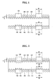
- a solar cell includes a substrate 110, an emitter layer 120 positioned at one surface of the substrate 110, for example, a front surface of the substrate 110, a first protective layer 130 positioned on the emitter layer 120, a first anti-reflection layer 140 positioned on the first protective layer 130, a plurality of first electrodes 150 positioned on the emitter layer 120 where the first protective layer 130 and the first anti-reflection layer 140 are not positioned, a back surface field (BSF) layer 160 positioned at a back surface of the substrate 110, a second protective layer 170 positioned on the back surface of the substrate 110, a second anti-reflection layer 180 positioned on a back surface of the second protective layer 170, and a plurality of second electrodes 190 positioned on a back surface of the back surface field layer 160 where the second protective layer 170 and the second anti-reflection layer 180 are not positioned.
- BSF back surface field
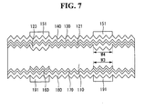
- the surface of the substrate 110 may be uniformly textured to form a textured surface corresponding to an uneven surface or having uneven characteristics. More specifically, the substrate 110 has a first textured surface 111 (refer to FIG. 3 ) corresponding to the front surface, at which the emitter layer 120 is positioned, and a second textured surface 113 (refer to FIG. 3 ) corresponding to the back surface opposite the front surface.
- the first protective layer 130 positioned on the emitter layer 120 formed at the front surface of the substrate 110 is formed of a material having negative fixed charges, for example, aluminum oxide (AlO x ) or yttrium oxide (Y 2 O 3 ).
- the material of the first protective layer 130 has excellent chemical passivation characteristic resulting from a low interface trap density and excellent field effect passivation characteristic resulting from the negative fixed charges. Further, the material is very excellent in stability, moisture transmission, and abrasion resistance. Thus, the first protective layer 130 reduces a surface recombination velocity, thereby improving the efficiency and the reliability of the solar cell.
- the first protective layer 130 is formed of a material having fixed charges of the same conductive type as the first conductive type.
- the light reflectance at the front surface of the substrate 110 represented a minimum value when the first protective layer 130 and the first anti-reflection layer 140 were within the above refractive index and thickness ranges.
- a silicon oxide layer having a thickness of about 1 nm to 3 nm may be further formed at an interface between the first protective layer 130 and the emitter layer 120.
- the first electrodes 150 may be formed using a plating process.
- the first electrode 150 may include a metal seed layer and a conductive layer plated on the metal seed layer.
- a diffusion prevention layer may be further formed between the metal seed layer and the conductive layer, thereby preventing a material forming the conductive layer from being diffused into the doped region through the metal seed layer.
- the second electrodes 190 may be formed of at least one conductive material selected from the group consisting of aluminum (Al), nickel (Ni), copper (Cu), silver (Ag), tin (Sn), zinc (Zn), indium (In), titanium (Ti), gold (Au), and a combination thereof.
- the second electrodes 190 are formed of a conductive paste obtained by mixing Ag with a glass frit.
- the second electrodes 190 may be formed using the plating process in the same manner as the first electrodes 150.
- the back surface field layer 160 electrically and physically connected to the second electrodes 190 is locally positioned at the back surface of the substrate 110 at the same location as the second electrodes 190.
- the back surface field layer 160 is a region (for example, n + -type region) that is more heavily doped than the substrate 110 with impurities of the same conductive type as the substrate 110.
- the back surface field layer 160 has a surface resistivity of about 30 ⁇ /sq to 80 ⁇ /sq.
- a width W3 of the back surface field layer 160 may be equal to or less than the width W2 of the second electrode 190 or may be greater than the width W2 of the second electrode 190.
- the movement of holes to the back surface of the substrate 110 is prevented or reduced by a potential barrier resulting from a difference between impurity concentrations of the substrate 110 and the back surface field layer 160. Hence, a recombination and/or a disappearance of electrons and holes around the surface of the substrate 110 are prevented or reduced.
- the second protective layer 170 and the second anti-reflection layer 180 are positioned on the back surface of the substrate 110 where the second electrodes 190 and the back surface field layer 160 are not positioned.
- the second protective layer 170 is formed of the same material as the first protective layer 130 and has the same thickness as the first protective layer 130.
- the second anti-reflection layer 180 is formed of the same material as the first anti-reflection layer 140 and has the same thickness as the first anti-reflection layer 140. Nevertheless, different materials or other materials may be used.
- the solar cell having the above-described structure according to the embodiment of the invention may serve as a double-sided (or bifacial) light receiving solar cell, and an operation of the solar cell is described below.
- the substrate 110 When light irradiated onto the solar cell is incident on the substrate 110 through the emitter layer 120 and/or the back surface of the substrate 110, a plurality of electron-hole pairs are generated in the substrate 110 by the light energy.
- the front surface and the back surface of the substrate 110 are the first textured surface 111 and the second textured surface 113, respectively, the light reflectance at each of the front surface and the back surface of the substrate 110 may be reduced.
- both a light incident operation and a light reflection operation may be performed on each of the first and second textured surfaces 111 and 113 of the substrate 110, light may be confined in the solar cell. Hence, light absorption may increase, and the efficiency of the solar cell may be improved.
- an amount of light incident on the substrate 110 may further increase.
- the electron-hole pairs are separated into electrons and holes by the p-n junction between the substrate 110 and the emitter layer 120, and the separated holes move to the p-type emitter layer 120 and the separated electrons move to the n-type substrate 110.
- the holes moving to the emitter layer 120 move to the first electrodes 150, and the electrons moving to the substrate 110 move to the second electrodes 190 through the back surface field layer 160. Accordingly, when the first electrodes 150 of one solar cell are connected to the second electrodes 190 of another solar cell adjacent to the one solar cell using electric wires such as interconnectors, electric current flows through the solar cells and allows use of the electric current for electric power.
- the solar cell having the above-described configuration may be used in a state where the solar cell is positioned between a light transmission front substrate and a light transmission back substrate and is sealed by a protective layer.
- a solar cell according to a second embodiment of the invention is described below with reference to FIG. 2 .
- the solar cell according to the second embodiment of the invention is substantially the same as the solar cell according to the first embodiment of the invention except an emitter layer, a further description may be briefly made or may be entirely omitted. Hereinafter, only a configuration of the emitter layer is described.
- the emitter layer 120 according to the first embodiment of the invention has a uniform doping concentration throughout the entire area of the emitter layer 120.
- the emitter layer 120 according to the first embodiment of the invention may be easily manufactured through a simple process, but a recombination of carriers of the emitter layer 120 may increase because of a high doping concentration. As a result, an improvement in the efficiency of the solar cell may be limited.
- the emitter layer 120 according to the second embodiment of the invention is configured so that the recombination of carriers of the emitter layer 120 is prevented or reduced. More specifically, the emitter layer 120 contacting first electrodes 150 is a heavily doped region, and the emitter layer 120 not contacting the first electrodes 150 is a lightly doped region.
- the emitter layer 120 includes a first doped region 121 corresponding to a lightly doped p-type region and a second doped region 123, which is more heavily doped than the first doped region 121 with p-type impurities.
- the second doped region 123 may be formed at the same location of the substrate 110 as the first electrodes 150.
- a width W4 of the second doped region 123 may be equal to or less than a width W1 of the first electrode 150 or may be greater than the width W1 of the first electrode 150.
- the first doped region 121 has a surface resistivity of about 80 ⁇ /sq to 200 ⁇ /sq
- the second doped region 123 has a surface resistivity of about 30 ⁇ /sq to 80 ⁇ /sq.
- the solar cell according to the second embodiment of the invention prevents or reduces the recombination of carriers, and thus the efficiency of the solar cell according to the second embodiment of the invention may be further improved.
- a method for manufacturing the solar cell according to the second embodiment of the invention is described below with reference to FIGS. 3 to 7 .
- a substrate 110 formed of a silicon wafer is generally manufactured by slicing a silicon block or an ingot using a blade or a multi-wire saw.
- the silicon wafer is prepared and then is doped with impurities of a group V element, for example, phosphorus (P) to manufacture the substrate 110 having resistivity of about 1 ⁇ cm 2 to 10 ⁇ cm 2 .
- a group V element for example, phosphorus (P)
- a mechanical damage layer may be formed in the silicon wafer.
- a wet etching process for removing the mechanical damage layer is performed, so as to prevent a reduction in characteristics of the solar cell resulting from the mechanical damage layer.
- An alkaline etchant or an acid etchant may be used in the wet etching process.
- the wet etching process or a dry plasma etching process is performed to form a first textured surface 111 in the front surface of the substrate 110 and a second textured surface 113 in the back surface of the substrate 110.
- impurities of a group III element are injected into one surface (for example, the first textured surface 111) of the substrate 110 using an ion implantation method to form an emitter layer 120.
- an amount of ions implanted into the substrate 110 and an ion implantation depth when the substrate 110 is doped with impurities using the ion implantation method are controlled more easily than when the substrate 110 is doped with impurities using a thermal diffusion method.
- the ion implantation depth may vary depending on an amount of ions produced in a process room, an ion implantation energy, and the like.
- the ion implantation energy may be about 100 KeV to 3 MeV
- the ion implantation depth based on the ion implantation energy of about 100 KeV to 3 MeV may be about 0.5 ⁇ m to 10 ⁇ m measured from the surface of the substrate 110.
- impurities are lightly injected into the entire front surface of the substrate 110 to form a first doped region 121.
- impurities are heavily injected into a portion (for example, an area to form first electrodes 150) of the front surface of the substrate 110 to form a second doped region 123.
- the first doped region 121 has the surface resistivity of about 80 ⁇ /sq to 200 ⁇ /sq
- the second doped region 123 has the surface resistivity of about 30 ⁇ /sq to 80 ⁇ /sq.
- the emitter layer 120 including the first doped region 121 and the second doped region 123 may be formed using the thermal diffusion method in another embodiment of the invention.
- Impurities of a group V element are injected into a portion (for example, an area to form second electrodes 190) of the other surface (for example, the second textured surface 113) of the substrate 110 to form a back surface field layer 160 having a surface resistivity of about 30 ⁇ /sq to 80 ⁇ /sq. Further, the ion implantation method may be used to form the back surface field layer 160 in the same manner as the emitter layer 120.
- first protective layer 130 and a second protective layer 170 are formed using a plasma enhanced chemical vapor deposition (PECVD) method, a sputtering method, or other methods.
- PECVD plasma enhanced chemical vapor deposition
- the first protective layer 130 and the second protective layer 170 are formed so that they have a refractive index of about 1.55 to 1.7 and a thickness of about 5 nm to 30 nm.
- a silicon oxide layer having a thickness of about 1 nm to 3 nm may be formed at interfaces between the first protective layer 130 and the substrate 110, and the second protective layer 170 and the substrate 110.
- silicon nitride SiN x
- the first anti-reflection layer 140 and the second anti-reflection layer. 180 may be formed using the PECVD method, the sputtering method, or other methods.
- the first anti-reflection layer 140 and the second anti-reflection layer 180 are formed so that they have a refractive index of about 1.9 to 2.3 and a thickness of about 50 nm to 100 nm.
- the second anti-reflection layer 180 formed on the back surface of the substrate 100 may be thicker than the first anti-reflection layer 140 formed on the front surface of the substrate 100.
- a first conductive paste 151 obtained by mixing a mixture (Ag:Al) of silver (Ag) and aluminum (Al) with a glass frit is printed on the front surface of the substrate 100 with a first electrode pattern
- a second conductive paste 191 obtained by mixing Ag with the glass frit is printed on the back surface of the substrate 100 with a second electrode pattern.
- a firing process is then performed on the first conductive paste 151 and the second conductive paste 191.
- the material of the protective layers 130 and 170 and the material of the anti-reflection layers 140 and 180 are etched by an etching component contained in the glass frit.
- the first electrodes 150 electrically and physically connected to the second doped region 123 of the emitter layer 120 are formed, and the second electrodes 190 electrically and physically connected to the back surface field layer 160 are formed.
- the first electrodes 150 and the second electrodes 190 may be formed using a plating process.
- a portion of the surface of the substrate 110 to form the first electrodes 150 and the second electrodes 190 has to be exposed so as to form the first electrodes 150 and the second electrodes 190 using the plating process.
- the same portion between the first protective layer 130 and the first anti-reflection layer 140 and the same portion between the second protective layer 170 and the second anti-reflection layer 180 may be removed using a dry etching process to form the first electrodes 150 and the second electrodes 190 on the removed portions of the surface of the substrate 110.
- a metal seed layer may be formed on the exposed portions of the surface of the substrate 110 and then a conductive layer or a diffusion prevention layer and a conductive layer may be formed on the metal seed layer.
- reference to fixed charges includes oxide fixed charges.
Landscapes
- Life Sciences & Earth Sciences (AREA)
- Sustainable Development (AREA)
- Engineering & Computer Science (AREA)
- Sustainable Energy (AREA)
- Photovoltaic Devices (AREA)
- Chemical & Material Sciences (AREA)
- Crystallography & Structural Chemistry (AREA)
Applications Claiming Priority (1)
| Application Number | Priority Date | Filing Date | Title |
|---|---|---|---|
| KR1020110005429A KR20120084104A (ko) | 2011-01-19 | 2011-01-19 | 태양전지 |
Publications (1)
| Publication Number | Publication Date |
|---|---|
| EP2479794A1 true EP2479794A1 (fr) | 2012-07-25 |
Family
ID=44510653
Family Applications (1)
| Application Number | Title | Priority Date | Filing Date |
|---|---|---|---|
| EP11006399A Ceased EP2479794A1 (fr) | 2011-01-19 | 2011-08-03 | Cellule solaire |
Country Status (4)
| Country | Link |
|---|---|
| US (5) | US9608133B2 (fr) |
| EP (1) | EP2479794A1 (fr) |
| KR (1) | KR20120084104A (fr) |
| CN (2) | CN107256893A (fr) |
Cited By (1)
| Publication number | Priority date | Publication date | Assignee | Title |
|---|---|---|---|---|
| EP4092764A1 (fr) | 2013-04-03 | 2022-11-23 | Lg Electronics Inc. | Cellule solaire |
Families Citing this family (27)
| Publication number | Priority date | Publication date | Assignee | Title |
|---|---|---|---|---|
| KR101258938B1 (ko) * | 2011-07-25 | 2013-05-07 | 엘지전자 주식회사 | 태양 전지 |
| KR101295552B1 (ko) * | 2011-11-16 | 2013-08-12 | 엘지전자 주식회사 | 태양 전지 및 그 제조 방법 |
| KR101307204B1 (ko) * | 2011-11-30 | 2013-09-11 | 엘지전자 주식회사 | 태양 전지 및 그 제조 방법 |
| KR101838278B1 (ko) * | 2011-12-23 | 2018-03-13 | 엘지전자 주식회사 | 태양 전지 |
| KR101958819B1 (ko) * | 2012-01-27 | 2019-03-15 | 엘지전자 주식회사 | 양면 수광형 태양전지의 제조 방법 |
| KR101879364B1 (ko) * | 2012-02-08 | 2018-07-18 | 엘지전자 주식회사 | 태양 전지 및 그 제조 방법 |
| KR101894585B1 (ko) * | 2012-02-13 | 2018-09-04 | 엘지전자 주식회사 | 태양전지 |
| TW201411866A (zh) * | 2012-09-07 | 2014-03-16 | Unitech Printed Circuit Board Corp | 太陽能電池背面鈍化局部擴散結構及其製造方法 |
| CN103178135B (zh) * | 2013-02-26 | 2015-10-14 | 友达光电股份有限公司 | 太阳能电池及其制作方法 |
| KR101631450B1 (ko) * | 2013-03-05 | 2016-06-17 | 엘지전자 주식회사 | 태양 전지 |
| KR101889774B1 (ko) * | 2013-09-09 | 2018-08-20 | 엘지전자 주식회사 | 태양 전지 |
| KR101699743B1 (ko) * | 2013-04-03 | 2017-02-13 | 엘지전자 주식회사 | 태양 전지 |
| KR20150035189A (ko) | 2013-09-27 | 2015-04-06 | 엘지전자 주식회사 | 태양 전지 |
| KR102120120B1 (ko) * | 2013-11-28 | 2020-06-08 | 엘지전자 주식회사 | 태양 전지 및 이의 제조 방법 |
| KR101614190B1 (ko) * | 2013-12-24 | 2016-04-20 | 엘지전자 주식회사 | 태양전지 및 이의 제조 방법 |
| KR101541252B1 (ko) | 2014-10-13 | 2015-08-04 | 한양대학교 에리카산학협력단 | 태양 전지 및 그 제조 방법 |
| KR20180100301A (ko) * | 2015-10-25 | 2018-09-10 | 솔라라운드 리미티드 | 양면형 전지 제조 방법 |
| CN105514187A (zh) * | 2016-01-13 | 2016-04-20 | 无锡尚德太阳能电力有限公司 | 太阳能电池结构及其制造方法 |
| EP3331029B1 (fr) * | 2016-12-02 | 2021-09-01 | LG Electronics Inc. | Cellule solaire en tandem et son procédé de fabrication |
| JP6792465B2 (ja) * | 2017-01-26 | 2020-11-25 | 信越化学工業株式会社 | 高光電変換効率太陽電池の製造方法 |
| DE102018108158B4 (de) * | 2018-04-06 | 2023-06-07 | Hanwha Q Cells Gmbh | Bifazial-Solarzelle, Solarmodul und Herstellungsverfahren für eine Bifazial-Solarzelle |
| CN108682701B (zh) * | 2018-05-07 | 2021-06-04 | 张家港协鑫集成科技有限公司 | 太阳能电池及其制作工艺 |
| US11145774B2 (en) * | 2018-05-30 | 2021-10-12 | Solar Inventions Llc | Configurable solar cells |
| KR102102823B1 (ko) * | 2018-10-30 | 2020-04-22 | 성균관대학교산학협력단 | 표면 구조를 이용한 선택적 에미터의 형성 방법 및 표면 구조를 이용한 선택적 에미터를 포함한 태양전지 |
| EP3971993A1 (fr) * | 2020-09-16 | 2022-03-23 | Jbao Technology Ltd. | Procédé de fabrication de la structure dorsale d'une cellule solaire double face de type p |
| CN114335197B (zh) * | 2022-03-11 | 2022-08-19 | 浙江爱旭太阳能科技有限公司 | 太阳能电池的导电接触结构、组件及发电系统 |
| CN119907343A (zh) * | 2025-03-27 | 2025-04-29 | 晶科能源(海宁)有限公司 | 光伏电池及其制造方法、光伏组件 |
Citations (11)
| Publication number | Priority date | Publication date | Assignee | Title |
|---|---|---|---|---|
| DE4217428A1 (de) * | 1991-12-09 | 1993-06-17 | Deutsche Aerospace | Hochleistungs-solarzellenstruktur |
| US20040112426A1 (en) * | 2002-12-11 | 2004-06-17 | Sharp Kabushiki Kaisha | Solar cell and method of manufacturing the same |
| EP1763086A1 (fr) * | 2005-09-09 | 2007-03-14 | Interuniversitair Micro-Elektronica Centrum | Cellule solaire avec une couche épaisse de passivation d'oxyde de silicium et de nitrure de silicium et son procédé de fabrication |
| US20070210395A1 (en) * | 2006-02-24 | 2007-09-13 | Yasushi Maruyama | Solid-state imaging device, method for producing same, and camera |
| EP1876650A1 (fr) * | 2005-04-26 | 2008-01-09 | Shin-Etsu Handotai Co., Ltd | Procédé de fabrication d une cellule solaire et cellule solaire |
| DE102007054384A1 (de) * | 2007-11-14 | 2009-05-20 | Institut Für Solarenergieforschung Gmbh | Verfahren zum Herstellen einer Solarzelle mit einer oberflächenpassivierenden Dielektrikumdoppelschicht und entsprechende Solarzelle |
| EP2077584A2 (fr) * | 2007-12-28 | 2009-07-08 | Industrial Technology Research Institute | Structure de couche de passivation de cellule solaire et son procédé de fabrication |
| WO2010003784A2 (fr) * | 2008-06-16 | 2010-01-14 | Institut Für Solarenergieforschung Gmbh | Cellule solaire au silicium à surface de type p passivée et son procédé de fabrication |
| WO2010111107A2 (fr) * | 2009-03-26 | 2010-09-30 | Bp Corporation North America Inc. | Appareil et procédé pour piles solaires à contacts formés par tir laser dans des régions dopées diffusées thermiquement |
| WO2011033826A1 (fr) * | 2009-09-18 | 2011-03-24 | 信越化学工業株式会社 | Cellule solaire, son procédé de fabrication et module de cellule solaire |
| US20110140226A1 (en) * | 2010-09-27 | 2011-06-16 | Yoonsil Jin | Semiconductor devices and methods for manufacturing the same |
Family Cites Families (18)
| Publication number | Priority date | Publication date | Assignee | Title |
|---|---|---|---|---|
| US4751191A (en) * | 1987-07-08 | 1988-06-14 | Mobil Solar Energy Corporation | Method of fabricating solar cells with silicon nitride coating |
| WO2005004198A2 (fr) * | 2003-06-13 | 2005-01-13 | North Carolina State University | Oxydes complexes pouvant etre utilises dans des dispositifs semi-conducteurs et procedes associes |
| JP4232597B2 (ja) | 2003-10-10 | 2009-03-04 | 株式会社日立製作所 | シリコン太陽電池セルとその製造方法 |
| US7144751B2 (en) * | 2004-02-05 | 2006-12-05 | Advent Solar, Inc. | Back-contact solar cells and methods for fabrication |
| CN101079967B (zh) | 2006-02-24 | 2013-07-10 | 索尼株式会社 | 固态成像装置及其制造方法、以及摄像机 |
| DE102007012277A1 (de) | 2007-03-08 | 2008-09-11 | Gebr. Schmid Gmbh & Co. | Verfahren zur Herstellung einer Solarzelle sowie damit hergestellte Solarzelle |
| KR101393353B1 (ko) * | 2007-10-29 | 2014-05-13 | 서울바이오시스 주식회사 | 발광다이오드 |
| KR20090078275A (ko) | 2008-01-14 | 2009-07-17 | 엘지전자 주식회사 | 요철 형태의 절연막을 포함하는 태양전지 및 그 제조방법 |
| KR20100096746A (ko) | 2009-02-25 | 2010-09-02 | 엘지전자 주식회사 | 태양전지 및 그의 제조방법 |
| CN102077359B (zh) | 2008-06-26 | 2012-10-03 | 三菱电机株式会社 | 太阳能电池单元及其制造方法 |
| KR101002282B1 (ko) | 2008-12-15 | 2010-12-20 | 엘지전자 주식회사 | 태양 전지 및 그 제조 방법 |
| KR101627217B1 (ko) | 2009-03-25 | 2016-06-03 | 엘지전자 주식회사 | 태양전지 및 그 제조방법 |
| EP4350782A3 (fr) * | 2009-04-21 | 2024-07-10 | Tetrasun, Inc. | Structures de cellules solaires à haut rendement et procédés de fabrication |
| US8298850B2 (en) * | 2009-05-01 | 2012-10-30 | Silicor Materials Inc. | Bifacial solar cells with overlaid back grid surface |
| KR101159277B1 (ko) | 2009-05-29 | 2012-06-22 | 주식회사 효성 | 강유전체를 이용한 태양전지의 제조방법 |
| KR101032624B1 (ko) * | 2009-06-22 | 2011-05-06 | 엘지전자 주식회사 | 태양 전지 및 그 제조 방법 |
| TW201121066A (en) * | 2009-12-14 | 2011-06-16 | Ind Tech Res Inst | Bificial solar cell |
| US8153456B2 (en) * | 2010-01-20 | 2012-04-10 | Varian Semiconductor Equipment Associates, Inc. | Bifacial solar cell using ion implantation |
-
2011
- 2011-01-19 KR KR1020110005429A patent/KR20120084104A/ko not_active Ceased
- 2011-07-13 US US13/182,203 patent/US9608133B2/en active Active
- 2011-08-03 EP EP11006399A patent/EP2479794A1/fr not_active Ceased
- 2011-09-22 CN CN201710389651.8A patent/CN107256893A/zh active Pending
- 2011-09-22 CN CN2011102829769A patent/CN102610664A/zh active Pending
-
2017
- 2017-02-27 US US15/443,331 patent/US10446697B2/en active Active
-
2019
- 2019-09-04 US US16/560,384 patent/US11538945B2/en active Active
-
2022
- 2022-10-05 US US17/960,545 patent/US12402436B2/en active Active
-
2024
- 2024-08-28 US US18/817,582 patent/US20240421238A1/en active Pending
Patent Citations (11)
| Publication number | Priority date | Publication date | Assignee | Title |
|---|---|---|---|---|
| DE4217428A1 (de) * | 1991-12-09 | 1993-06-17 | Deutsche Aerospace | Hochleistungs-solarzellenstruktur |
| US20040112426A1 (en) * | 2002-12-11 | 2004-06-17 | Sharp Kabushiki Kaisha | Solar cell and method of manufacturing the same |
| EP1876650A1 (fr) * | 2005-04-26 | 2008-01-09 | Shin-Etsu Handotai Co., Ltd | Procédé de fabrication d une cellule solaire et cellule solaire |
| EP1763086A1 (fr) * | 2005-09-09 | 2007-03-14 | Interuniversitair Micro-Elektronica Centrum | Cellule solaire avec une couche épaisse de passivation d'oxyde de silicium et de nitrure de silicium et son procédé de fabrication |
| US20070210395A1 (en) * | 2006-02-24 | 2007-09-13 | Yasushi Maruyama | Solid-state imaging device, method for producing same, and camera |
| DE102007054384A1 (de) * | 2007-11-14 | 2009-05-20 | Institut Für Solarenergieforschung Gmbh | Verfahren zum Herstellen einer Solarzelle mit einer oberflächenpassivierenden Dielektrikumdoppelschicht und entsprechende Solarzelle |
| EP2077584A2 (fr) * | 2007-12-28 | 2009-07-08 | Industrial Technology Research Institute | Structure de couche de passivation de cellule solaire et son procédé de fabrication |
| WO2010003784A2 (fr) * | 2008-06-16 | 2010-01-14 | Institut Für Solarenergieforschung Gmbh | Cellule solaire au silicium à surface de type p passivée et son procédé de fabrication |
| WO2010111107A2 (fr) * | 2009-03-26 | 2010-09-30 | Bp Corporation North America Inc. | Appareil et procédé pour piles solaires à contacts formés par tir laser dans des régions dopées diffusées thermiquement |
| WO2011033826A1 (fr) * | 2009-09-18 | 2011-03-24 | 信越化学工業株式会社 | Cellule solaire, son procédé de fabrication et module de cellule solaire |
| US20110140226A1 (en) * | 2010-09-27 | 2011-06-16 | Yoonsil Jin | Semiconductor devices and methods for manufacturing the same |
Non-Patent Citations (14)
| Title |
|---|
| "Handbook of Photovoltaic Science and Engineering", 25 April 2003, JOHN WILEY & SONS, LTD, Chichester, UK, ISBN: 978-0-47-149196-5, article IGNACIO TOBÍAS ET AL: "Crystalline Silicon Solar Cells and Modules", pages: 255 - 306, XP055056057, DOI: 10.1002/0470014008.ch7 * |
| "Novel cost-effective bifacial silicon solar cells with 19.4% front and 18.1% rear efficiency", APPLIED PHYSICS LETTERS, AIP, AMERICAN INSTITUTE OF PHYSICS, MELVILLE, NY, US, vol. 70, no. 8, 24 February 1997 (1997-02-24), pages 1008, XP012018380, ISSN: 0003-6951, DOI: 10.1063/1.118466 * |
| ARUMUGHAN J ET AL: "Realization of Thin MC-Silicon Pert-Type Bifacial Solar Cells in Industrial Environments", CONFERENCE RECORD OF THE 2006 IEEE 4TH WORLD CONFERENCE ON PHOTOVOLTAIC ENERGY CONVERSION (IEEE CAT. NO.06CH37747), IEEE, 1 May 2006 (2006-05-01), pages 1103 - 1106, XP031007502, ISBN: 978-1-4244-0016-4 * |
| G. DINGEMANS ET AL: "Recent Progress in the Development and Understanding of Silicon Surface Passivation by Aluminum Oxide for Photovoltaics", 25TH EUROPEAN PHOTOVOLTAIC SOLAR ENERGY CONFERENCE AND EXHIBITION / 5TH WORLD CONFERENCE ON PHOTOVOLTAIC ENERGY CONVERSION, VALENCIA, SPAIN, 1 January 2010 (2010-01-01), pages 1083 - 1090, XP055010434 * |
| GLUNZ S W ET AL: "Analysis of laser-fired local back surface fields using n<+>np<+> cell structures", PROCEEDINGS OF THE 3RD WORLD CONFERENCE ON PHOTOVOLTAIC ENERGY CONVERSION : JOINT CONFERENCE OF 13TH PV SCIENCE & ENGINEERING CONFERENCE, 30TH IEEE PV SPECIALISTS CONFERENCE, 18TH EUROPEAN PV SOLAR ENERGY CONFERENCE; OSAKA INTERNATIONAL CONGRESS CENT, 18 May 2003 (2003-05-18), pages 1332 - 1335Vol.2, XP031988020, ISBN: 978-4-9901816-0-4 * |
| HOEX B ET AL: "Excellent passivation of highly doped p-type Si surfaces by the negative-charge-dielectric Al2O3", APPLIED PHYSICS LETTERS, AMERICAN INSTITUTE OF PHYSICS, US, vol. 91, no. 11, 11 September 2007 (2007-09-11), pages 112107 - 112107, XP012099144, ISSN: 0003-6951, DOI: 10.1063/1.2784168 * |
| JAN SCHMIDT ET AL: "Effective surface passivation of crystalline silicon using ultrathin Al 2 O 3 films and Al 2 O 3 /SiN x stacks", PHYSICA STATUS SOLIDI (RRL) - RAPID RESEARCH LETTERS, 17 September 2009 (2009-09-17), pages 287 - 289, XP055011115, ISSN: 1862-6254, DOI: 10.1002/pssr.200903272 * |
| KNOBLOCH J ET AL: "High-efficiency solar cells from FZ, CZ and MC silicon material", PROCEEDINGS OF THE PHOTOVOLTAIC SPECIALISTS CONFERENCE. LOUISVILLE, MAY 10 - 14, 1993; [PROCEEDINGS OF THE PHOTOVOLTAIC SPECIALISTS CONFERENCE], NEW YORK, IEEE, US, vol. CONF. 23, 10 May 1993 (1993-05-10), pages 271 - 276, XP010113395, ISBN: 978-0-7803-1220-3, DOI: 10.1109/PVSC.1993.347172 * |
| KRANZL A ET AL: "Bifacial Solar Cells on Multi-Crystalline Silicon with Boron BSF and Open Rear Contact", PHOTOVOLTAIC ENERGY CONVERSION, CONFERENCE RECORD OF THE 2006 IEEE 4TH WORLD CONFERENCE ON, IEEE, PI, 1 May 2006 (2006-05-01), pages 968 - 971, XP031007467, ISBN: 978-1-4244-0016-4 * |
| MIHAILETCHI VALENTIN ET AL: "Nitric acid pretreatment for the passivation of boron emitters for n-type base silicon solar cells", APPLIED PHYSICS LETTERS, AMERICAN INSTITUTE OF PHYSICS, US, vol. 92, no. 6, 14 February 2008 (2008-02-14), pages 63510 - 63510, XP012108251, ISSN: 0003-6951, DOI: 10.1063/1.2870202 * |
| TUCCI M ET AL: "Laser fired back contact for silicon solar cells", THIN SOLID FILMS, ELSEVIER-SEQUOIA S.A. LAUSANNE, CH, vol. 516, no. 20, 30 August 2008 (2008-08-30), pages 6767 - 6770, XP022777851, ISSN: 0040-6090, [retrieved on 20071215], DOI: 10.1016/J.TSF.2007.12.079 * |
| WEISKRICHER ET AL: "The refractive index of thin Al2O3 films", VACUUM, PERGAMON PRESS, GB, vol. 2, no. 1, 1 January 1952 (1952-01-01), pages 89, XP025579636, ISSN: 0042-207X, [retrieved on 19520101], DOI: 10.1016/0042-207X(52)90310-2 * |
| WOLF S: "Thermal Oxidation of Silicon", SILICON PROCESSING FOR THE VLSI ERA,, vol. 1, 1 January 2000 (2000-01-01), pages 265 - 323, XP001525854 * |
| YOON ET AL: "Refractive index and etched structure of silicon nitride waveguides fabricated by PECVD", THIN SOLID FILMS, ELSEVIER-SEQUOIA S.A. LAUSANNE, CH, vol. 515, no. 12, 23 April 2007 (2007-04-23), pages 5004 - 5007, XP022212172, ISSN: 0040-6090, DOI: 10.1016/J.TSF.2006.10.059 * |
Cited By (2)
| Publication number | Priority date | Publication date | Assignee | Title |
|---|---|---|---|---|
| EP4092764A1 (fr) | 2013-04-03 | 2022-11-23 | Lg Electronics Inc. | Cellule solaire |
| EP4092757A1 (fr) | 2013-04-03 | 2022-11-23 | Lg Electronics Inc. | Procédé de fabrication d'une cellule solaire |
Also Published As
| Publication number | Publication date |
|---|---|
| US12402436B2 (en) | 2025-08-26 |
| US20230023738A1 (en) | 2023-01-26 |
| US20190393366A1 (en) | 2019-12-26 |
| US10446697B2 (en) | 2019-10-15 |
| KR20120084104A (ko) | 2012-07-27 |
| CN107256893A (zh) | 2017-10-17 |
| US20110265870A1 (en) | 2011-11-03 |
| US9608133B2 (en) | 2017-03-28 |
| US20170170340A1 (en) | 2017-06-15 |
| US20240421238A1 (en) | 2024-12-19 |
| US11538945B2 (en) | 2022-12-27 |
| CN102610664A (zh) | 2012-07-25 |
Similar Documents
| Publication | Publication Date | Title |
|---|---|---|
| US12402436B2 (en) | Solar cell | |
| US11056598B2 (en) | Solar cell | |
| US10680122B2 (en) | Solar cell and method for manufacturing the same | |
| KR101661768B1 (ko) | 태양전지 및 이의 제조 방법 | |
| EP2622644B1 (fr) | Dispositifs semi-conducteurs et leurs procédés de fabrication | |
| EP2219222B1 (fr) | Cellule solaire et son procédé de fabrication | |
| KR101614190B1 (ko) | 태양전지 및 이의 제조 방법 | |
| US9997647B2 (en) | Solar cells and manufacturing method thereof | |
| KR101166361B1 (ko) | 태양전지 | |
| EP2903037B1 (fr) | Procédé de fabrication d' une cellule solaire à contact arrière à hétérojonction | |
| KR101708242B1 (ko) | 태양전지 및 이의 제조 방법 | |
| KR101757887B1 (ko) | 태양전지 | |
| KR101757880B1 (ko) | 태양전지 | |
| KR102120120B1 (ko) | 태양 전지 및 이의 제조 방법 |
Legal Events
| Date | Code | Title | Description |
|---|---|---|---|
| PUAI | Public reference made under article 153(3) epc to a published international application that has entered the european phase |
Free format text: ORIGINAL CODE: 0009012 |
|
| 17P | Request for examination filed |
Effective date: 20110803 |
|
| AK | Designated contracting states |
Kind code of ref document: A1 Designated state(s): AL AT BE BG CH CY CZ DE DK EE ES FI FR GB GR HR HU IE IS IT LI LT LU LV MC MK MT NL NO PL PT RO RS SE SI SK SM TR |
|
| AX | Request for extension of the european patent |
Extension state: BA ME |
|
| 17Q | First examination report despatched |
Effective date: 20121102 |
|
| APBK | Appeal reference recorded |
Free format text: ORIGINAL CODE: EPIDOSNREFNE |
|
| APBN | Date of receipt of notice of appeal recorded |
Free format text: ORIGINAL CODE: EPIDOSNNOA2E |
|
| APBR | Date of receipt of statement of grounds of appeal recorded |
Free format text: ORIGINAL CODE: EPIDOSNNOA3E |
|
| APAF | Appeal reference modified |
Free format text: ORIGINAL CODE: EPIDOSCREFNE |
|
| APBT | Appeal procedure closed |
Free format text: ORIGINAL CODE: EPIDOSNNOA9E |
|
| APBV | Interlocutory revision of appeal recorded |
Free format text: ORIGINAL CODE: EPIDOSNIRAPE |
|
| STAA | Information on the status of an ep patent application or granted ep patent |
Free format text: STATUS: THE APPLICATION HAS BEEN REFUSED |
|
| 18R | Application refused |
Effective date: 20191211 |