EP2480918B1 - Lich temittierende vorrichtung mit einer lichtleiterplatte mit reflektierender abschirmung mit verringerter blendung - Google Patents
Lich temittierende vorrichtung mit einer lichtleiterplatte mit reflektierender abschirmung mit verringerter blendung Download PDFInfo
- Publication number
- EP2480918B1 EP2480918B1 EP10763016.2A EP10763016A EP2480918B1 EP 2480918 B1 EP2480918 B1 EP 2480918B1 EP 10763016 A EP10763016 A EP 10763016A EP 2480918 B1 EP2480918 B1 EP 2480918B1
- Authority
- EP
- European Patent Office
- Prior art keywords
- light
- guide plate
- emitting device
- light guide
- light emitting
- Prior art date
- Legal status (The legal status is an assumption and is not a legal conclusion. Google has not performed a legal analysis and makes no representation as to the accuracy of the status listed.)
- Not-in-force
Links
- 230000004313 glare Effects 0.000 title description 10
- 230000003287 optical effect Effects 0.000 claims description 48
- 239000000758 substrate Substances 0.000 claims description 15
- 238000010168 coupling process Methods 0.000 claims description 13
- 238000005859 coupling reaction Methods 0.000 claims description 13
- 230000004907 flux Effects 0.000 claims description 12
- 239000000463 material Substances 0.000 description 9
- 238000000605 extraction Methods 0.000 description 3
- 238000005286 illumination Methods 0.000 description 3
- 239000011230 binding agent Substances 0.000 description 2
- 239000003086 colorant Substances 0.000 description 2
- 238000009826 distribution Methods 0.000 description 2
- 229910052751 metal Inorganic materials 0.000 description 2
- 239000002184 metal Substances 0.000 description 2
- 239000002245 particle Substances 0.000 description 2
- 229920006254 polymer film Polymers 0.000 description 2
- NIXOWILDQLNWCW-UHFFFAOYSA-N acrylic acid group Chemical group C(C=C)(=O)O NIXOWILDQLNWCW-UHFFFAOYSA-N 0.000 description 1
- 229910052782 aluminium Inorganic materials 0.000 description 1
- XAGFODPZIPBFFR-UHFFFAOYSA-N aluminium Chemical compound [Al] XAGFODPZIPBFFR-UHFFFAOYSA-N 0.000 description 1
- 230000000903 blocking effect Effects 0.000 description 1
- 230000003247 decreasing effect Effects 0.000 description 1
- 230000000694 effects Effects 0.000 description 1
- 238000005265 energy consumption Methods 0.000 description 1
- 238000005516 engineering process Methods 0.000 description 1
- 230000002708 enhancing effect Effects 0.000 description 1
- 239000004973 liquid crystal related substance Substances 0.000 description 1
- 238000004519 manufacturing process Methods 0.000 description 1
- 150000002739 metals Chemical class 0.000 description 1
- 238000012986 modification Methods 0.000 description 1
- 230000004048 modification Effects 0.000 description 1
- 229920000515 polycarbonate Polymers 0.000 description 1
- 239000004417 polycarbonate Substances 0.000 description 1
- 229920000307 polymer substrate Polymers 0.000 description 1
- 230000000750 progressive effect Effects 0.000 description 1
- 230000003746 surface roughness Effects 0.000 description 1
Images

Classifications
-
- G—PHYSICS
- G02—OPTICS
- G02B—OPTICAL ELEMENTS, SYSTEMS OR APPARATUS
- G02B6/00—Light guides; Structural details of arrangements comprising light guides and other optical elements, e.g. couplings
- G02B6/0001—Light guides; Structural details of arrangements comprising light guides and other optical elements, e.g. couplings specially adapted for lighting devices or systems
- G02B6/0011—Light guides; Structural details of arrangements comprising light guides and other optical elements, e.g. couplings specially adapted for lighting devices or systems the light guides being planar or of plate-like form
- G02B6/0013—Means for improving the coupling-in of light from the light source into the light guide
- G02B6/0015—Means for improving the coupling-in of light from the light source into the light guide provided on the surface of the light guide or in the bulk of it
- G02B6/0018—Redirecting means on the surface of the light guide
-
- G—PHYSICS
- G02—OPTICS
- G02B—OPTICAL ELEMENTS, SYSTEMS OR APPARATUS
- G02B6/00—Light guides; Structural details of arrangements comprising light guides and other optical elements, e.g. couplings
- G02B6/0001—Light guides; Structural details of arrangements comprising light guides and other optical elements, e.g. couplings specially adapted for lighting devices or systems
- G02B6/0011—Light guides; Structural details of arrangements comprising light guides and other optical elements, e.g. couplings specially adapted for lighting devices or systems the light guides being planar or of plate-like form
- G02B6/0033—Means for improving the coupling-out of light from the light guide
- G02B6/005—Means for improving the coupling-out of light from the light guide provided by one optical element, or plurality thereof, placed on the light output side of the light guide
- G02B6/0055—Reflecting element, sheet or layer
-
- G—PHYSICS
- G02—OPTICS
- G02B—OPTICAL ELEMENTS, SYSTEMS OR APPARATUS
- G02B6/00—Light guides; Structural details of arrangements comprising light guides and other optical elements, e.g. couplings
- G02B6/0001—Light guides; Structural details of arrangements comprising light guides and other optical elements, e.g. couplings specially adapted for lighting devices or systems
- G02B6/0011—Light guides; Structural details of arrangements comprising light guides and other optical elements, e.g. couplings specially adapted for lighting devices or systems the light guides being planar or of plate-like form
- G02B6/0066—Light guides; Structural details of arrangements comprising light guides and other optical elements, e.g. couplings specially adapted for lighting devices or systems the light guides being planar or of plate-like form characterised by the light source being coupled to the light guide
- G02B6/0073—Light emitting diode [LED]
-
- F—MECHANICAL ENGINEERING; LIGHTING; HEATING; WEAPONS; BLASTING
- F21—LIGHTING
- F21V—FUNCTIONAL FEATURES OR DETAILS OF LIGHTING DEVICES OR SYSTEMS THEREOF; STRUCTURAL COMBINATIONS OF LIGHTING DEVICES WITH OTHER ARTICLES, NOT OTHERWISE PROVIDED FOR
- F21V13/00—Producing particular characteristics or distribution of the light emitted by means of a combination of elements specified in two or more of main groups F21V1/00 - F21V11/00
- F21V13/12—Combinations of only three kinds of elements
-
- F—MECHANICAL ENGINEERING; LIGHTING; HEATING; WEAPONS; BLASTING
- F21—LIGHTING
- F21Y—INDEXING SCHEME ASSOCIATED WITH SUBCLASSES F21K, F21L, F21S and F21V, RELATING TO THE FORM OR THE KIND OF THE LIGHT SOURCES OR OF THE COLOUR OF THE LIGHT EMITTED
- F21Y2115/00—Light-generating elements of semiconductor light sources
- F21Y2115/10—Light-emitting diodes [LED]
-
- G—PHYSICS
- G02—OPTICS
- G02B—OPTICAL ELEMENTS, SYSTEMS OR APPARATUS
- G02B6/00—Light guides; Structural details of arrangements comprising light guides and other optical elements, e.g. couplings
- G02B6/0001—Light guides; Structural details of arrangements comprising light guides and other optical elements, e.g. couplings specially adapted for lighting devices or systems
- G02B6/0011—Light guides; Structural details of arrangements comprising light guides and other optical elements, e.g. couplings specially adapted for lighting devices or systems the light guides being planar or of plate-like form
- G02B6/0066—Light guides; Structural details of arrangements comprising light guides and other optical elements, e.g. couplings specially adapted for lighting devices or systems the light guides being planar or of plate-like form characterised by the light source being coupled to the light guide
- G02B6/0068—Arrangements of plural sources, e.g. multi-colour light sources
Definitions
- the present invention relates to light emitting devices and more specifically to light emitting devices comprising light guides making use of total internal reflection (TIR).
- TIR total internal reflection
- Light emitting devices of the kind referred to here generally consist of one or more light emitting diodes (LEDs) and a light guiding plate attached in connection to the LEDs.
- the light guiding layer of these known light emitting devices further comprises a number of optical structures for out-coupling of light on a light emitting surface thereof.
- a problem with this type of light emitting devices is that the use of LEDs causes glare problems in some situations, for example when being used for lighting purposes in offices and other working places.
- European Union regulations limit the luminance exposed to an observer to ⁇ 10 3 cd/m 2 in most sensible directions (from 90° to 65° with vertical) and to ⁇ 10 4 cd/m 2 in other directions.
- the light guide plate is adapted to provide a certain degree of glare protection by reduction of the extraction of light by the light extracting structures.
- glare problems would arise.
- one or more LEDs were to be removed or if one or more LEDs would fail, the corresponding array element/elements would turn substantially darker than adjacent ones since each array element is exposed directly to a corresponding LED.
- Document EP 1 640 756 A1 discloses an indirect backlight illumination system comprising a plurality of light sources (102) and light guiding means (104) for a liquid crystal display.
- the light guiding means has a first surface providing a structured surface pattern (106), through which light is coupled out, and a second surface opposite to the first surface, comprising recesses (108) and light blocking means (110).
- the backlight illumination system provides good colour mixing while still having a reasonable backlight thickness.
- a light emitting device comprising a plurality of light sources and a light guide plate.
- the light guide plate has a light exit surface and an opposed light entrance surface facing the plurality of light sources.
- the light entrance surface is arranged for in-coupling of light emitted by the light sources into the light guide plate. At least part of the in-coupled light is transmitted within the light guide plate by total internal reflection so that light from different light sources is mixed within the light guide plate. At least part of the light exit surface is provided with an optical structure for out-coupling of light.
- the light emitting device further comprises a reflective shielding provided at positions where the flux of the direct light of the light sources towards the light guide plate have their maximum density in a powered state of the light sources.
- a reflective shielding provided at positions where the flux of the direct light of the light sources towards the light guide plate have their maximum density in a powered state of the light sources.
- the reflective shielding is provided at the light entrance surface of the light guide plate at positions where the flux of the direct light of the light sources towards the light guide plate have their maximum density in a powered state of the light sources.
- a reflective shielding can easily be provided at the light entrance surface of the light guide plate during manufacture thereof.
- the light sources are mounted on a substrate and wherein a surface of the substrate facing the light guide plate is provided with reflective shielding. Light which has been reflected towards the light source will be reflected back towards the light guide plate, thereby enhancing the optical efficiency and mixing of the light emitted by different light sources.
- the mixing averages differences in color temperature and flux of the light sources, thereby increasing binning tolerances for the light emitting device.
- a plurality of optical structures are provided as separate exit windows over the light exit surface of the light guide plate and at least a part of the non-structured area of the light exit surface of the light guide plate is flat.
- a roughness is introduced into a part of the flat light exit surface of the light guide plate in order to provide secondary out-coupling of light.
- the light guide plate is connected to the substrate by way of side walls arranged along an outer edge of the light guide plate, and wherein inner surfaces of the side walls are provided with reflective shielding.
- the reflective shielding enhances the optical efficiency and mixing of the light within the light emitting device.
- the side walls are arranged such that lateral surfaces of the light guide plate are exposed.
- lateral surfaces of the light guide plate By leaving lateral surfaces of the light guide plate exposed, it is possible to couple a plurality of light emitting devices to each other in such that light will be transmitted between the light guide plates of the different light emitting devices.
- the side walls are arranged such that they cover lateral surfaces of the light guide plate.
- the light sources comprise light emitting diodes.
- the optical structure comprises conical lenses.
- the optical structure comprises elements having a pyramidal shape.
- the optical structure comprises diffusive elements.
- the optical structure comprises a refractive collimating structure.
- reflective shielding is provided at the light guide plate such that at least 10% and not more than 90% of the area of the light exit surface of the light guide plate is shielded.
- a luminaire comprising such a light emitting device.
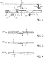
- FIG. 1 shows a light emitting device 100 in accordance with an embodiment of the present invention.
- the light emitting device 100 comprises a substrate 3 made from any suitable material such as aluminum, or another metal, or a polymer substrate.
- a plurality of light sources 2, in this case LEDs, are attached to the lower side of the substrate 3 and are adapted to generate light downwards in the direction of light exit windows of the light emitting device 100. This provides for a good thermal efficiency since the heat generated by the LEDs can exit the light emitting device 100 upwards.
- a light guide plate 4 is arranged below and substantially parallel to the substrate 3.
- This light guide plate 4 is made from translucent material such as e.g. acrylic or polycarbonate.
- the light exit surface of the light guide plate 4 is provided with one or more optical structures 6 for out-coupling of light. These optical structures 6 are formed as individual light exit windows over the light exit surface of the light guide plate.
- the optical structures 6 can be provided in the form of for example conical lenses or pyramids and can have varying sizes and light extracting properties in order to create different light distributions, e.g. general light and wall illumination at the same time from the same lighting fixture.
- a reflective shielding 5 is arranged at the light entrance surface of the light guide plate 4 at positions were the flux of the direct light of the light sources towards the light guide plate 4 have their maximum density in a powered state of the light sources.
- the reflective shielding 5 may for example include a metalized layer, a binding agent with reflecting particles, a dielectric multi stack layer or a reflective polymer film. Since the light guide plate 4 is shielded at positions where the flux of the light sources have their maximum density, the reflective shielding 5 will also ensure an efficient glare protection.
- the light L1, L2 generated by the light sources can be divided into three different parts, wherein one part L11,L21 is transmitted and redirected by the optical structure 6, a second part L12, L22 is reflected back towards the light source and the third part L13, L23 is in-coupled into the light guide plate 4 where it can travel through the light guide plate 4 and mix with light from other light sources and eventually exit the light guide plate 4 through any of the optical structures 6 provided over the light exit surface of the light guide plate.
- the light L12, L22 which is reflected back towards the light sources 2 will be redirected again towards the light guide plate 4 by the substrate 3. This provides for an effective mixing of light from different light sources 2 even before it has been in-coupled into the light guide plate.
- the light sources 2 may have different brightness and colors, can be effectively decreased. Also, thanks to the fact that the light sources 2 are hidden behind reflective shielding 5 a LED failure will hardly be visible and will not appear as one optical structure becoming substantially darker than the other. Instead, a failure of a separate LED in a device according to the invention will appear as a minor reduction in light intensity from all optical structures 6 or at least from a number of optical structures within an area. It should be noted that the reflective shielding 5 does not necessarily have to be arranged on the light guide plate 4 itself. As long as it is positioned were the flux of the direct light of the light sources towards the light guide plate 4 have their maximum density in a powered state of the light sources it can be arranged anywhere between the light sources 2 and the light exit surface of the light guide plate 4.
- FIG 2 an embodiment 200 is shown where the optical structure 6 is provided at lower position than the rest of the light exit surface of the light guide plate 4.
- the reflective shielding 7 on the light exit surface of the light guide plate 4 instead of at the light entrance surface it can be ensured that the light will exit the light guide plate 4 only at the optical structure 6 and at the same time the total thickness of the light guide plate 4 can be kept constant.
- Figure 3 shows an embodiment 300 of the light guide plate 4 where a controlled roughness 8 has been introduced into the flat part of the light exit surface of the light guide plate 4.
- This roughness 8 serves as a secondary light extraction surface and can be shaped as a logotype, a company name or any other desired shape.
- This secondary light extraction surface will generally not provide a luminance as intense as the optical structure 6, but will give more of a glowing appearance. It is also possible to vary the roughness 8 over the surface in order to create different patterns. Together with the possibility of using different types of optical structures 6 this provides for a very high degree of design freedom. It is also possible to provide such a controlled roughness over the whole non-structured surface of the light guide plate 4 and if it is desirable to extract light in the opposite direction, a surface roughness may also be provided on the light entrance side of the light guide plate 4.
- Figure 4 shows two different optical structures 6 which will create different light distributions. These are merely two examples from a very broad range of possible structures and the figure is intended to show the principle of having different types of optical structures at different locations of the light exit surface of the light guide plate.
- FIG. 5 shows a light emitting device 600 in accordance with an embodiment of the present invention.
- reflective shielding 5 is provided on the light entrance surface of the light guide plate 4 at positions where the flux of the direct light of the LEDs towards the light guide plate 4 have their maximum density in a powered state of the LEDs.
- the provision of a reflective shielding to re-direct the light at this position is an effective measure to avoid glare problems.
- the reflective shielding can be adapted to form any suitable cone angle.
- the reflective shielding 5 is individually adapted to each LED 2.
- the translucent material of the light guide plate 4 will decrease the observed luminance and provide sufficient glare protection.
- the combination of a shield just below the LED with the progressive de-glaring qualities of the translucent material for laterally emitted intensities provides a very effective de-glaring concept.
- the reflective shielding 5 does not necessarily have to be arranged directly to the light guide plate 4.
- an indirect component is desirable, to create e.g. a ceiling brightness or similar. This can be achieved by providing light emitting islands of light guiding material in the substrate 3.
- the out-coupling of light from the light guiding material can be achieved either with optical structures or by introducing a roughness into a surface of the light guiding material.
- side walls 9 are provided along the outer edges of the light guide plate 4 and the substrate 3 connecting them to each other.
- the inner surfaces of the side walls 9 as well as the lower surface of the substrate 3 are also provided with reflective shielding 5.
- the reflective shielding 5 can include e.g. a metalized layer, a binding agent with reflecting particles or a reflective polymer film.
- the reflective shielding may, however, may also be obtained by choosing suitable materials for the substrate 3 and the inner walls 9. Examples of suitable materials include metals which, if necessary, have the surface in question treated to obtain good reflective properties.
- each optical structure is positioned in front of a LED and most of the light emitted by the LED will be transmitted directly to the outside world. The light emitted by the separate optical structures in that prior art will therefore be perceived by an observer as having different colors and intensities.
- a light emitting device may form one luminaire.
- a plurality of light emitting devices 600 can be placed against each other to form one luminaire consisting of a plurality of separate light emitting devices 600. If necessary, e.g. of energy consumption reasons or simply while less light is desirable, one or more of the separate light emitting devices can be switched off. Since the side walls 9 are arranged on top of the light guide plate 4 to leave the lateral surfaces of the light guide plate 4 exposed and due to the light guiding effect, the light emitting areas of the switched off devices will not turn black but still emit a glow of light. If, however, a single light emitting device 600 is intended to be used, the side walls 9 could be arranged to cover the lateral surfaces of the light guide plate 4.
- Figures 6a-6f are merely intended to present a few of the many exit window patterns allowed by this optical concept.
- the grey areas are light emitting areas formed by optical structures 6.
- Figure 6a shows an exit window pattern comprising a square-shaped optical structure enclosed in another optical structure 6 having the shape of a hollow quadrangle.
- Figure 6b shows an exit window pattern comprising a plurality of circular optical structures 6 evenly distributed over the surface of the light guide plate 4.
- Figure 6c shows an exit window pattern comprising a plurality of circular optical structures 6 arranged in groups of six, wherein each group depicts a more of less circular pattern.
- Figure 6d shows an exit window pattern comprising a plurality square-shaped optical structures 6 evenly distributed over the surface of the light guide plate 4.
- Figure 6e shows an exit window pattern comprising a plurality of circular optical structures 6 arranged in groups of four, wherein each group depicts a tilted square.
- Figure 6f shows an exit window pattern comprising a circular optical structure enclosed in another optical structure 6 shaped as a hollow circle.
- one housing can be equipped with more or less LEDs for different applications. And since the LED technology development constantly increases flux per LED values, it is necessary to be able to continuously adapt the system. Also, the positioning of the LEDs in a light emitting device according to this invention is more or less irrelevant, especially with respect to the optical structures, as long as the cone angles are respected, which allows for a simple and robust architecture with low tolerance requirements.
- the light guide plate does not have to be flat but can instead have a curved form.
- LEDs instead of using LEDs as light sources, it would also be possible to use OLED strips as light source.
Landscapes
- Physics & Mathematics (AREA)
- General Physics & Mathematics (AREA)
- Optics & Photonics (AREA)
- Engineering & Computer Science (AREA)
- Microelectronics & Electronic Packaging (AREA)
- Planar Illumination Modules (AREA)
- Non-Portable Lighting Devices Or Systems Thereof (AREA)
- Light Guides In General And Applications Therefor (AREA)
Claims (14)
- Licht emittierende Vorrichtung (100, 600) mit mehreren Lichtquellen (2) und einer Lichtleiterplatte (4), wobei die Lichtleiterplatte (4) eine Lichtaustrittsfläche und eine gegenüberliegende, den mehreren Lichtquellen (2) zugewandte Lichteintrittsfläche aufweist, wobei die Lichteintrittsfläche so angeordnet ist, dass sie von den Lichtquellen (2) abgestrahltes Licht in die Lichtleiterplatte (4) einkoppelt, wobei zumindest ein Teil des eingekoppelten Lichts innerhalb der Lichtleiterplatte (4) durch innere Totalreflexion übertragen wird, so dass Licht von verschiedenen Lichtquellen (2) innerhalb der Lichtleiterplatte (4) gemischt wird, und wobei zumindest ein Teil der Lichtaustrittsfläche mit einer optischen Struktur (6) zur Auskopplung von Licht versehen ist, und wobei die Licht emittierende Vorrichtung (100, 600) weiterhin eine reflektive Abschirmung (5) umfasst, die an Positionen vorgesehen ist, an denen der Fluss des direkten Lichts der Lichtquellen (2) zu der Lichtleiterplatte (4) hin seine maximale Dichte in einem betriebenen Zustand der Lichtquellen (2) aufweist,
wobei mehrere optische Strukturen (6) als separate Austrittsfenster über der Lichtaustrittsfläche der Lichtleiterplatte (4) vorgesehen sind, und wobei zumindest ein Teil der nicht-strukturierten Fläche der Lichtaustrittsfläche der Lichtleiterplatte (4) flach ist, wobei die reflektive Abschirmung auf der Lichtleiterplatte entweder auf der flachen, nicht-strukturierten Fläche der Lichtaustrittsfläche oder auf der Lichteintrittsfläche gegenüber der flachen, nicht-strukturierten Fläche der Lichtaustrittsfläche angebracht ist. - Licht emittierende Vorrichtung nach Anspruch 1, wobei die reflektive Abschirmung (5) an der Lichteintrittsfläche der Lichtleiterplatte (4) an Positionen vorgesehen ist, an denen der Fluss des direkten Lichts der Lichtquellen zu der Lichtleiterplatte (4) hin seine maximale Dichte in einem betriebenen Zustand der Lichtquellen aufweist.
- Licht emittierende Vorrichtung nach einem der vorangegangenen Ansprüche, wobei die Lichtquellen (2) auf einem Substrat (3) angebracht sind, und wobei eine, der Lichtleiterplatte (4) zugewandte Oberfläche des Substrats (3) mit einer reflektiven Abschirmung (5) versehen ist.
- Licht emittierende Vorrichtung nach Anspruch 1, wobei in einen Teil der flachen Lichtaustrittsfläche der Lichtleiterplatte (4) eine Rauigkeit eingebracht wird, um eine sekundäre Auskopplung von Licht vorzusehen.
- Licht emittierende Vorrichtung nach einem der vorangegangenen Ansprüche, wobei die Lichtleiterplatte (4) mit Hilfe von entlang einem äußeren Rand der Lichtleiterplatte (4) angeordneten Seitenwänden (9) mit dem Substrat (3) verbunden ist, und wobei Innenflächen der Seitenwände (9) mit einer reflektiven Abschirmung (5) versehen sind.
- Licht emittierende Vorrichtung nach Anspruch 5, wobei die Seitenwände (9) so angeordnet sind, dass laterale Oberflächen der Lichtleiterplatte (4) freigelegt werden.
- Licht emittierende Vorrichtung nach Anspruch 5, wobei die Seitenwände (9) so angeordnet sind, dass sie laterale Oberflächen der Lichtleiterplatte (4) bedecken.
- Licht emittierende Vorrichtung nach Anspruch 1, wobei die Lichtquellen (2) Licht emittierende Dioden umfassen.
- Licht emittierende Vorrichtung nach Anspruch 1, wobei die optische Struktur (6) konische Linsen umfasst.
- Licht emittierende Vorrichtung nach Anspruch 1, wobei die optische Struktur (6) Elemente mit einer pyramidenartigen Form umfasst.
- Licht emittierende Vorrichtung nach Anspruch 1, wobei die optische Struktur (6) ein diffusives Element umfasst.
- Licht emittierende Vorrichtung nach Anspruch 1, wobei die optische Struktur (6) eine refraktive, kollimierende Struktur umfasst.
- Licht emittierende Vorrichtung nach Anspruch 2, wobei die reflektive Abschirmung (5) an der Lichtleiterplatte (4) so vorgesehen ist, dass mindestens 10% und nicht mehr als 90% der Fläche der Lichtaustrittsfläche der Lichtleiterplatte (4) abgeschirmt sind.
- Leuchte mit einer Licht emittierenden Vorrichtung nach einem der Ansprüche 1-13.
Priority Applications (1)
| Application Number | Priority Date | Filing Date | Title |
|---|---|---|---|
| EP10763016.2A EP2480918B8 (de) | 2009-09-21 | 2010-09-09 | Lich temittierende vorrichtung mit einer lichtleiterplatte mit reflektierender abschirmung mit verringerter blendung |
Applications Claiming Priority (3)
| Application Number | Priority Date | Filing Date | Title |
|---|---|---|---|
| EP09170790 | 2009-09-21 | ||
| EP10763016.2A EP2480918B8 (de) | 2009-09-21 | 2010-09-09 | Lich temittierende vorrichtung mit einer lichtleiterplatte mit reflektierender abschirmung mit verringerter blendung |
| PCT/IB2010/054057 WO2011033424A1 (en) | 2009-09-21 | 2010-09-09 | Light emitting device comprising a light guide plate with reflective shielding with glare reduction |
Publications (3)
| Publication Number | Publication Date |
|---|---|
| EP2480918A1 EP2480918A1 (de) | 2012-08-01 |
| EP2480918B1 true EP2480918B1 (de) | 2016-07-20 |
| EP2480918B8 EP2480918B8 (de) | 2016-09-21 |
Family
ID=43309506
Family Applications (1)
| Application Number | Title | Priority Date | Filing Date |
|---|---|---|---|
| EP10763016.2A Not-in-force EP2480918B8 (de) | 2009-09-21 | 2010-09-09 | Lich temittierende vorrichtung mit einer lichtleiterplatte mit reflektierender abschirmung mit verringerter blendung |
Country Status (5)
| Country | Link |
|---|---|
| US (1) | US8721101B2 (de) |
| EP (1) | EP2480918B8 (de) |
| JP (1) | JP2013505549A (de) |
| CN (1) | CN102511012B (de) |
| WO (1) | WO2011033424A1 (de) |
Cited By (1)
| Publication number | Priority date | Publication date | Assignee | Title |
|---|---|---|---|---|
| TWI827475B (zh) * | 2023-02-23 | 2023-12-21 | 群光電子股份有限公司 | 具有發光功能之電子裝置 |
Families Citing this family (24)
| Publication number | Priority date | Publication date | Assignee | Title |
|---|---|---|---|---|
| US10977965B2 (en) | 2010-01-29 | 2021-04-13 | Avery Dennison Retail Information Services, Llc | Smart sign box using electronic interactions |
| EP3133579B1 (de) | 2010-01-29 | 2020-03-04 | Avery Dennison Corporation | Intelligente schilderbox mit elektronischen interaktionen |
| KR101830718B1 (ko) * | 2011-07-15 | 2018-02-22 | 엘지이노텍 주식회사 | 디스플레이 장치 |
| US9858583B2 (en) | 2011-09-01 | 2018-01-02 | Avery Dennison Retail Information Services, Llc | Apparatus, system and method for tracking consumer product interest using mobile devices |
| US8630908B2 (en) | 2011-11-02 | 2014-01-14 | Avery Dennison Corporation | Distributed point of sale, electronic article surveillance, and product information system, apparatus and method |
| EP2828573B1 (de) * | 2012-03-18 | 2017-05-10 | Robe Lighting, Inc | Verbessertes kollimationssystem für eine led-leuchte |
| US8934173B2 (en) | 2012-08-21 | 2015-01-13 | Svv Technology Innovations, Inc. | Optical article for illuminating building interiors with sunlight |
| CN104025129B (zh) | 2012-09-10 | 2018-04-03 | 艾利丹尼森公司 | 用于防止nfc签条未授权转移的方法 |
| EP2786304B1 (de) | 2012-10-18 | 2017-06-07 | Avery Dennison Corporation | Verfahren, system und vorrichtung für nfc-sicherheit |
| WO2014064582A1 (en) | 2012-10-26 | 2014-05-01 | Koninklijke Philips N.V. | Lighting device and lighting system |
| ES2698060T3 (es) | 2012-11-19 | 2019-01-30 | Avery Dennison Corp | Sistema de seguridad NFC y método para deshabilitar etiquetas no autorizadas |
| JP6231133B2 (ja) * | 2013-01-25 | 2017-11-15 | フィリップス ライティング ホールディング ビー ヴィ | 照明装置及び照明システム |
| DE102013106689B4 (de) * | 2013-06-26 | 2022-02-03 | OSRAM Opto Semiconductors Gesellschaft mit beschränkter Haftung | Optoelektronisches Halbleiterbauteil |
| JP2015022799A (ja) * | 2013-07-16 | 2015-02-02 | 東洋電装株式会社 | スイッチ装置 |
| AT515640A1 (de) * | 2014-03-31 | 2015-10-15 | Werner Färber | Beleuchtungsvorrichtung |
| JP6367608B2 (ja) * | 2014-05-19 | 2018-08-01 | 矢崎総業株式会社 | 車両用表示装置 |
| KR102278308B1 (ko) * | 2014-10-15 | 2021-07-19 | 삼성디스플레이 주식회사 | 백라이트 유닛 및 이를 포함한 표시장치 |
| AT16410U1 (de) * | 2015-10-09 | 2019-08-15 | Zumtobel Lighting Gmbh | Anordnung zur flächigen Lichtabgabe |
| US10553766B2 (en) * | 2016-03-16 | 2020-02-04 | Lumileds Holding B.V. | Method of manufacturing an LED module |
| WO2017182392A1 (en) * | 2016-04-22 | 2017-10-26 | Philips Lighting Holding B.V. | Pebble-plate like louvre |
| US10649130B2 (en) | 2016-04-22 | 2020-05-12 | Signify Holding B.V. | Pebble-plate like louvre with specific domain characteristics |
| US11506832B2 (en) * | 2019-02-21 | 2022-11-22 | Minebea Mitsumi Inc. | Planar illumination device with light guide plate with pseudo light sources |
| FR3105357B1 (fr) | 2019-12-19 | 2022-01-07 | Gilbert Paulezec | Panneau de couverture lumineux et ensemble le comprenant |
| US11835213B2 (en) * | 2021-08-19 | 2023-12-05 | Matthew Hartley | Lighting fixtures with improved lighting components |
Family Cites Families (29)
| Publication number | Priority date | Publication date | Assignee | Title |
|---|---|---|---|---|
| US5386347A (en) | 1992-10-02 | 1995-01-31 | Photo Craft Co., Ltd. | Illuminating apparatus and a method of manufacturing an edge light conductor for use therein |
| US6301002B1 (en) * | 1993-12-22 | 2001-10-09 | Eastman Kodak Company | Film holder |
| JP3521058B2 (ja) * | 1998-06-12 | 2004-04-19 | 株式会社エンプラス | 導光板、サイドライト型面光源装置及び液晶表示装置 |
| EP1153240B1 (de) | 1999-02-24 | 2003-11-19 | 3M Innovative Properties Company | Beleuchtungsvorrichtung zur herstellung vorherbestimmten intensitätsmustern |
| DE10102586A1 (de) * | 2001-01-20 | 2002-07-25 | Philips Corp Intellectual Pty | Beleuchtungseinrichtung mit punktförmigen Lichtquellen |
| DE10102585A1 (de) * | 2001-01-20 | 2002-07-25 | Philips Corp Intellectual Pty | Farbige Beleuchtungseinrichtung |
| JP4397728B2 (ja) * | 2004-04-21 | 2010-01-13 | 日東電工株式会社 | 直下型バックライト |
| US7997771B2 (en) | 2004-06-01 | 2011-08-16 | 3M Innovative Properties Company | LED array systems |
| KR20060012959A (ko) * | 2004-08-05 | 2006-02-09 | 삼성전자주식회사 | 표시 장치용 백라이트 |
| TWI249257B (en) * | 2004-09-24 | 2006-02-11 | Epistar Corp | Illumination apparatus |
| EP1640756A1 (de) * | 2004-09-27 | 2006-03-29 | Barco N.V. | Methode und System zur Beleuchtung |
| KR101189080B1 (ko) * | 2005-01-24 | 2012-11-09 | 삼성디스플레이 주식회사 | 반사판과 이를 포함하는 액정표시장치 |
| KR101174770B1 (ko) * | 2005-02-28 | 2012-08-17 | 엘지디스플레이 주식회사 | 백라이트 유닛 및 이를 이용한 액정표시장치 |
| JP4655746B2 (ja) * | 2005-04-27 | 2011-03-23 | ソニー株式会社 | バックライト装置及び表示装置 |
| JP2006344409A (ja) * | 2005-06-07 | 2006-12-21 | Seiko Instruments Inc | 照明装置及びこれを備える表示装置 |
| KR20080055840A (ko) * | 2005-09-15 | 2008-06-19 | 니폰 제온 가부시키가이샤 | 직하형 백라이트 장치 |
| JP4280283B2 (ja) | 2006-01-27 | 2009-06-17 | 株式会社オプトデザイン | 面照明光源装置及びこれを用いた面照明装置 |
| JP2007227286A (ja) * | 2006-02-27 | 2007-09-06 | Seiko Instruments Inc | 照明装置、及びこれを用いた表示装置 |
| CN101126822B (zh) * | 2006-08-18 | 2010-09-29 | 鸿富锦精密工业(深圳)有限公司 | 光学板及采用该光学板的背光模组 |
| WO2008047284A2 (en) | 2006-10-16 | 2008-04-24 | Koninklijke Philips Electronics N.V. | Flat and thin led-based luminary |
| US20080089093A1 (en) * | 2006-10-17 | 2008-04-17 | Miller Anne M | Backlight unit using particular direct backlight assembly |
| EP2089745A1 (de) | 2006-11-28 | 2009-08-19 | Koninklijke Philips Electronics N.V. | Lichtführungsschicht mit integriertem misch- und lichtextraktionsbereich |
| TW200825529A (en) * | 2006-12-06 | 2008-06-16 | Chi Lin Technology Co Ltd | Light mixer and backlight module having it |
| CN101308225B (zh) * | 2007-05-18 | 2011-07-27 | 鸿富锦精密工业(深圳)有限公司 | 背光模组及其光学板 |
| US20090086508A1 (en) * | 2007-09-27 | 2009-04-02 | Philips Lumileds Lighting Company, Llc | Thin Backlight Using Low Profile Side Emitting LEDs |
| US7791683B2 (en) | 2007-11-19 | 2010-09-07 | Honeywell International Inc. | Backlight systems for liquid crystal displays |
| GB2448564B (en) * | 2007-11-26 | 2009-04-29 | Iti Scotland Ltd | Light guides |
| DE102007057671A1 (de) * | 2007-11-30 | 2009-06-04 | Osram Opto Semiconductors Gmbh | Beleuchtungsvorrichtung |
| JP2009283438A (ja) * | 2007-12-07 | 2009-12-03 | Sony Corp | 照明装置、表示装置、照明装置の製造方法 |
-
2010
- 2010-09-09 JP JP2012530379A patent/JP2013505549A/ja active Pending
- 2010-09-09 EP EP10763016.2A patent/EP2480918B8/de not_active Not-in-force
- 2010-09-09 US US13/496,937 patent/US8721101B2/en not_active Expired - Fee Related
- 2010-09-09 WO PCT/IB2010/054057 patent/WO2011033424A1/en not_active Ceased
- 2010-09-09 CN CN201080042017.3A patent/CN102511012B/zh not_active Expired - Fee Related
Cited By (2)
| Publication number | Priority date | Publication date | Assignee | Title |
|---|---|---|---|---|
| TWI827475B (zh) * | 2023-02-23 | 2023-12-21 | 群光電子股份有限公司 | 具有發光功能之電子裝置 |
| US11947155B1 (en) | 2023-02-23 | 2024-04-02 | Chicony Electronics Co., Ltd. | Electronic device with light emitting function |
Also Published As
| Publication number | Publication date |
|---|---|
| JP2013505549A (ja) | 2013-02-14 |
| US8721101B2 (en) | 2014-05-13 |
| EP2480918B8 (de) | 2016-09-21 |
| CN102511012B (zh) | 2014-10-15 |
| WO2011033424A1 (en) | 2011-03-24 |
| US20120176813A1 (en) | 2012-07-12 |
| CN102511012A (zh) | 2012-06-20 |
| EP2480918A1 (de) | 2012-08-01 |
Similar Documents
| Publication | Publication Date | Title |
|---|---|---|
| EP2480918B1 (de) | Lich temittierende vorrichtung mit einer lichtleiterplatte mit reflektierender abschirmung mit verringerter blendung | |
| JP5342016B2 (ja) | 大面積光パネル及びスクリーン | |
| US10670794B2 (en) | Illuminating device | |
| EP2067065B1 (de) | Beleuchtungssystem, leuchte und anzeigevorrichtung | |
| US12242100B2 (en) | Wide-area illumination system for displaying image prints in high contrast | |
| EP2696135B1 (de) | Beleuchtungsvorrichtung | |
| EP2082160B1 (de) | Dünne beleuchtungsvorrichtung, anzeigevorrichtung und leuchtvorrichtung | |
| EP2946138B1 (de) | Lichtemittierendes modul mit gebogener prismenfolie | |
| KR20120042845A (ko) | Led 기반의 램프 및 광 방출 사이니지 | |
| JP2010518617A (ja) | 少なくとも1つのledを含む照明デバイス | |
| WO2014172147A2 (en) | Lighting assembly | |
| TW201202624A (en) | Edge-light type lighting device | |
| EP2314911A2 (de) | Lichtquellenvorrichtung | |
| TWI572810B (zh) | Lighting device | |
| TW201135294A (en) | Lighting apparatus and light guide plate | |
| US20100066941A1 (en) | Hybrid lighting panel and lcd system | |
| WO2017172870A1 (en) | Illumination assembly providing backlight | |
| EP3551930B1 (de) | Leuchtdiodenbasierte lichtquelle mit lichtleiter | |
| CN102748677A (zh) | 背光模块 | |
| WO2018013535A1 (en) | Light guide having three-dimensional appearance and lighting assembly including same | |
| KR100810754B1 (ko) | 발광 유니트 및 이를 채용한 면발광 조립체 | |
| JP2014022125A (ja) | Led導光板光源によるled照明装置 | |
| JP2011009198A (ja) | Led照明装置 | |
| JP2013134888A (ja) | 照明装置および表示装置 | |
| KR102092881B1 (ko) | 조명 장치 |
Legal Events
| Date | Code | Title | Description |
|---|---|---|---|
| PUAI | Public reference made under article 153(3) epc to a published international application that has entered the european phase |
Free format text: ORIGINAL CODE: 0009012 |
|
| 17P | Request for examination filed |
Effective date: 20120423 |
|
| AK | Designated contracting states |
Kind code of ref document: A1 Designated state(s): AL AT BE BG CH CY CZ DE DK EE ES FI FR GB GR HR HU IE IS IT LI LT LU LV MC MK MT NL NO PL PT RO SE SI SK SM TR |
|
| DAX | Request for extension of the european patent (deleted) | ||
| RAP1 | Party data changed (applicant data changed or rights of an application transferred) |
Owner name: KONINKLIJKE PHILIPS N.V. |
|
| REG | Reference to a national code |
Ref country code: DE Ref legal event code: R079 Ref document number: 602010034876 Country of ref document: DE Free format text: PREVIOUS MAIN CLASS: G02B0006000000 Ipc: F21V0008000000 |
|
| GRAP | Despatch of communication of intention to grant a patent |
Free format text: ORIGINAL CODE: EPIDOSNIGR1 |
|
| RIC1 | Information provided on ipc code assigned before grant |
Ipc: F21V 13/12 20060101ALN20160223BHEP Ipc: F21V 8/00 20060101AFI20160223BHEP |
|
| RIC1 | Information provided on ipc code assigned before grant |
Ipc: F21V 13/12 20060101ALN20160229BHEP Ipc: F21V 8/00 20060101AFI20160229BHEP |
|
| INTG | Intention to grant announced |
Effective date: 20160316 |
|
| GRAS | Grant fee paid |
Free format text: ORIGINAL CODE: EPIDOSNIGR3 |
|
| GRAA | (expected) grant |
Free format text: ORIGINAL CODE: 0009210 |
|
| AK | Designated contracting states |
Kind code of ref document: B1 Designated state(s): AL AT BE BG CH CY CZ DE DK EE ES FI FR GB GR HR HU IE IS IT LI LT LU LV MC MK MT NL NO PL PT RO SE SI SK SM TR |
|
| REG | Reference to a national code |
Ref country code: GB Ref legal event code: FG4D |
|
| REG | Reference to a national code |
Ref country code: CH Ref legal event code: EP |
|
| REG | Reference to a national code |
Ref country code: IE Ref legal event code: FG4D |
|
| REG | Reference to a national code |
Ref country code: AT Ref legal event code: REF Ref document number: 814416 Country of ref document: AT Kind code of ref document: T Effective date: 20160815 |
|
| RAP2 | Party data changed (patent owner data changed or rights of a patent transferred) |
Owner name: PHILIPS LIGHTING HOLDING B.V. |
|
| REG | Reference to a national code |
Ref country code: DE Ref legal event code: R096 Ref document number: 602010034876 Country of ref document: DE |
|
| REG | Reference to a national code |
Ref country code: FR Ref legal event code: PLFP Year of fee payment: 7 |
|
| REG | Reference to a national code |
Ref country code: LT Ref legal event code: MG4D |
|
| REG | Reference to a national code |
Ref country code: NL Ref legal event code: MP Effective date: 20160720 |
|
| REG | Reference to a national code |
Ref country code: AT Ref legal event code: MK05 Ref document number: 814416 Country of ref document: AT Kind code of ref document: T Effective date: 20160720 |
|
| PG25 | Lapsed in a contracting state [announced via postgrant information from national office to epo] |
Ref country code: NL Free format text: LAPSE BECAUSE OF FAILURE TO SUBMIT A TRANSLATION OF THE DESCRIPTION OR TO PAY THE FEE WITHIN THE PRESCRIBED TIME-LIMIT Effective date: 20160720 Ref country code: NO Free format text: LAPSE BECAUSE OF FAILURE TO SUBMIT A TRANSLATION OF THE DESCRIPTION OR TO PAY THE FEE WITHIN THE PRESCRIBED TIME-LIMIT Effective date: 20161020 Ref country code: LT Free format text: LAPSE BECAUSE OF FAILURE TO SUBMIT A TRANSLATION OF THE DESCRIPTION OR TO PAY THE FEE WITHIN THE PRESCRIBED TIME-LIMIT Effective date: 20160720 Ref country code: IS Free format text: LAPSE BECAUSE OF FAILURE TO SUBMIT A TRANSLATION OF THE DESCRIPTION OR TO PAY THE FEE WITHIN THE PRESCRIBED TIME-LIMIT Effective date: 20161120 Ref country code: HR Free format text: LAPSE BECAUSE OF FAILURE TO SUBMIT A TRANSLATION OF THE DESCRIPTION OR TO PAY THE FEE WITHIN THE PRESCRIBED TIME-LIMIT Effective date: 20160720 Ref country code: FI Free format text: LAPSE BECAUSE OF FAILURE TO SUBMIT A TRANSLATION OF THE DESCRIPTION OR TO PAY THE FEE WITHIN THE PRESCRIBED TIME-LIMIT Effective date: 20160720 Ref country code: IT Free format text: LAPSE BECAUSE OF FAILURE TO SUBMIT A TRANSLATION OF THE DESCRIPTION OR TO PAY THE FEE WITHIN THE PRESCRIBED TIME-LIMIT Effective date: 20160720 |
|
| PG25 | Lapsed in a contracting state [announced via postgrant information from national office to epo] |
Ref country code: PT Free format text: LAPSE BECAUSE OF FAILURE TO SUBMIT A TRANSLATION OF THE DESCRIPTION OR TO PAY THE FEE WITHIN THE PRESCRIBED TIME-LIMIT Effective date: 20161121 Ref country code: SE Free format text: LAPSE BECAUSE OF FAILURE TO SUBMIT A TRANSLATION OF THE DESCRIPTION OR TO PAY THE FEE WITHIN THE PRESCRIBED TIME-LIMIT Effective date: 20160720 Ref country code: PL Free format text: LAPSE BECAUSE OF FAILURE TO SUBMIT A TRANSLATION OF THE DESCRIPTION OR TO PAY THE FEE WITHIN THE PRESCRIBED TIME-LIMIT Effective date: 20160720 Ref country code: BE Free format text: LAPSE BECAUSE OF NON-PAYMENT OF DUE FEES Effective date: 20160720 Ref country code: AT Free format text: LAPSE BECAUSE OF FAILURE TO SUBMIT A TRANSLATION OF THE DESCRIPTION OR TO PAY THE FEE WITHIN THE PRESCRIBED TIME-LIMIT Effective date: 20160720 Ref country code: ES Free format text: LAPSE BECAUSE OF FAILURE TO SUBMIT A TRANSLATION OF THE DESCRIPTION OR TO PAY THE FEE WITHIN THE PRESCRIBED TIME-LIMIT Effective date: 20160720 Ref country code: GR Free format text: LAPSE BECAUSE OF FAILURE TO SUBMIT A TRANSLATION OF THE DESCRIPTION OR TO PAY THE FEE WITHIN THE PRESCRIBED TIME-LIMIT Effective date: 20161021 Ref country code: LV Free format text: LAPSE BECAUSE OF FAILURE TO SUBMIT A TRANSLATION OF THE DESCRIPTION OR TO PAY THE FEE WITHIN THE PRESCRIBED TIME-LIMIT Effective date: 20160720 |
|
| REG | Reference to a national code |
Ref country code: DE Ref legal event code: R097 Ref document number: 602010034876 Country of ref document: DE |
|
| PG25 | Lapsed in a contracting state [announced via postgrant information from national office to epo] |
Ref country code: MC Free format text: LAPSE BECAUSE OF FAILURE TO SUBMIT A TRANSLATION OF THE DESCRIPTION OR TO PAY THE FEE WITHIN THE PRESCRIBED TIME-LIMIT Effective date: 20160720 Ref country code: EE Free format text: LAPSE BECAUSE OF FAILURE TO SUBMIT A TRANSLATION OF THE DESCRIPTION OR TO PAY THE FEE WITHIN THE PRESCRIBED TIME-LIMIT Effective date: 20160720 Ref country code: RO Free format text: LAPSE BECAUSE OF FAILURE TO SUBMIT A TRANSLATION OF THE DESCRIPTION OR TO PAY THE FEE WITHIN THE PRESCRIBED TIME-LIMIT Effective date: 20160720 |
|
| REG | Reference to a national code |
Ref country code: CH Ref legal event code: PL |
|
| PLBE | No opposition filed within time limit |
Free format text: ORIGINAL CODE: 0009261 |
|
| STAA | Information on the status of an ep patent application or granted ep patent |
Free format text: STATUS: NO OPPOSITION FILED WITHIN TIME LIMIT |
|
| PG25 | Lapsed in a contracting state [announced via postgrant information from national office to epo] |
Ref country code: BG Free format text: LAPSE BECAUSE OF FAILURE TO SUBMIT A TRANSLATION OF THE DESCRIPTION OR TO PAY THE FEE WITHIN THE PRESCRIBED TIME-LIMIT Effective date: 20161020 Ref country code: SM Free format text: LAPSE BECAUSE OF FAILURE TO SUBMIT A TRANSLATION OF THE DESCRIPTION OR TO PAY THE FEE WITHIN THE PRESCRIBED TIME-LIMIT Effective date: 20160720 Ref country code: SK Free format text: LAPSE BECAUSE OF FAILURE TO SUBMIT A TRANSLATION OF THE DESCRIPTION OR TO PAY THE FEE WITHIN THE PRESCRIBED TIME-LIMIT Effective date: 20160720 Ref country code: DK Free format text: LAPSE BECAUSE OF FAILURE TO SUBMIT A TRANSLATION OF THE DESCRIPTION OR TO PAY THE FEE WITHIN THE PRESCRIBED TIME-LIMIT Effective date: 20160720 Ref country code: CZ Free format text: LAPSE BECAUSE OF FAILURE TO SUBMIT A TRANSLATION OF THE DESCRIPTION OR TO PAY THE FEE WITHIN THE PRESCRIBED TIME-LIMIT Effective date: 20160720 |
|
| 26N | No opposition filed |
Effective date: 20170421 |
|
| REG | Reference to a national code |
Ref country code: IE Ref legal event code: MM4A |
|
| PG25 | Lapsed in a contracting state [announced via postgrant information from national office to epo] |
Ref country code: CH Free format text: LAPSE BECAUSE OF NON-PAYMENT OF DUE FEES Effective date: 20160930 Ref country code: LI Free format text: LAPSE BECAUSE OF NON-PAYMENT OF DUE FEES Effective date: 20160930 Ref country code: IE Free format text: LAPSE BECAUSE OF NON-PAYMENT OF DUE FEES Effective date: 20160909 |
|
| PG25 | Lapsed in a contracting state [announced via postgrant information from national office to epo] |
Ref country code: SI Free format text: LAPSE BECAUSE OF FAILURE TO SUBMIT A TRANSLATION OF THE DESCRIPTION OR TO PAY THE FEE WITHIN THE PRESCRIBED TIME-LIMIT Effective date: 20160720 Ref country code: LU Free format text: LAPSE BECAUSE OF NON-PAYMENT OF DUE FEES Effective date: 20160909 |
|
| REG | Reference to a national code |
Ref country code: FR Ref legal event code: PLFP Year of fee payment: 8 |
|
| PGFP | Annual fee paid to national office [announced via postgrant information from national office to epo] |
Ref country code: GB Payment date: 20170929 Year of fee payment: 8 |
|
| PGFP | Annual fee paid to national office [announced via postgrant information from national office to epo] |
Ref country code: DE Payment date: 20171130 Year of fee payment: 8 Ref country code: FR Payment date: 20171002 Year of fee payment: 8 |
|
| PG25 | Lapsed in a contracting state [announced via postgrant information from national office to epo] |
Ref country code: CY Free format text: LAPSE BECAUSE OF FAILURE TO SUBMIT A TRANSLATION OF THE DESCRIPTION OR TO PAY THE FEE WITHIN THE PRESCRIBED TIME-LIMIT Effective date: 20160720 Ref country code: HU Free format text: LAPSE BECAUSE OF FAILURE TO SUBMIT A TRANSLATION OF THE DESCRIPTION OR TO PAY THE FEE WITHIN THE PRESCRIBED TIME-LIMIT; INVALID AB INITIO Effective date: 20100909 |
|
| PG25 | Lapsed in a contracting state [announced via postgrant information from national office to epo] |
Ref country code: TR Free format text: LAPSE BECAUSE OF FAILURE TO SUBMIT A TRANSLATION OF THE DESCRIPTION OR TO PAY THE FEE WITHIN THE PRESCRIBED TIME-LIMIT Effective date: 20160720 Ref country code: MK Free format text: LAPSE BECAUSE OF FAILURE TO SUBMIT A TRANSLATION OF THE DESCRIPTION OR TO PAY THE FEE WITHIN THE PRESCRIBED TIME-LIMIT Effective date: 20160720 Ref country code: MT Free format text: LAPSE BECAUSE OF NON-PAYMENT OF DUE FEES Effective date: 20160930 |
|
| PG25 | Lapsed in a contracting state [announced via postgrant information from national office to epo] |
Ref country code: AL Free format text: LAPSE BECAUSE OF FAILURE TO SUBMIT A TRANSLATION OF THE DESCRIPTION OR TO PAY THE FEE WITHIN THE PRESCRIBED TIME-LIMIT Effective date: 20160720 |
|
| REG | Reference to a national code |
Ref country code: DE Ref legal event code: R119 Ref document number: 602010034876 Country of ref document: DE |
|
| GBPC | Gb: european patent ceased through non-payment of renewal fee |
Effective date: 20180909 |
|
| PG25 | Lapsed in a contracting state [announced via postgrant information from national office to epo] |
Ref country code: DE Free format text: LAPSE BECAUSE OF NON-PAYMENT OF DUE FEES Effective date: 20190402 |
|
| PG25 | Lapsed in a contracting state [announced via postgrant information from national office to epo] |
Ref country code: FR Free format text: LAPSE BECAUSE OF NON-PAYMENT OF DUE FEES Effective date: 20180930 |
|
| PG25 | Lapsed in a contracting state [announced via postgrant information from national office to epo] |
Ref country code: GB Free format text: LAPSE BECAUSE OF NON-PAYMENT OF DUE FEES Effective date: 20180909 |