EP2482449B1 - Circuit d'amplification avec optimisation de la puissance - Google Patents
Circuit d'amplification avec optimisation de la puissance Download PDFInfo
- Publication number
- EP2482449B1 EP2482449B1 EP11368002.9A EP11368002A EP2482449B1 EP 2482449 B1 EP2482449 B1 EP 2482449B1 EP 11368002 A EP11368002 A EP 11368002A EP 2482449 B1 EP2482449 B1 EP 2482449B1
- Authority
- EP
- European Patent Office
- Prior art keywords
- transistor
- power
- source
- gate
- drain
- Prior art date
- Legal status (The legal status is an assumption and is not a legal conclusion. Google has not performed a legal analysis and makes no representation as to the accuracy of the status listed.)
- Active
Links
- 230000003321 amplification Effects 0.000 title claims description 21
- 238000003199 nucleic acid amplification method Methods 0.000 title claims description 21
- 238000005457 optimization Methods 0.000 title 1
- 239000003990 capacitor Substances 0.000 claims description 10
- 238000012935 Averaging Methods 0.000 claims description 3
- 241001125929 Trisopterus luscus Species 0.000 description 6
- 230000006835 compression Effects 0.000 description 4
- 238000007906 compression Methods 0.000 description 4
- 230000006399 behavior Effects 0.000 description 3
- 230000007423 decrease Effects 0.000 description 3
- 238000013461 design Methods 0.000 description 3
- 230000003044 adaptive effect Effects 0.000 description 2
- 238000004891 communication Methods 0.000 description 2
- 238000000034 method Methods 0.000 description 2
- 101150004367 Il4i1 gene Proteins 0.000 description 1
- 230000003213 activating effect Effects 0.000 description 1
- 238000010276 construction Methods 0.000 description 1
- 230000000593 degrading effect Effects 0.000 description 1
- 238000001514 detection method Methods 0.000 description 1
- 238000011161 development Methods 0.000 description 1
- 238000005516 engineering process Methods 0.000 description 1
- 238000009499 grossing Methods 0.000 description 1
- 238000010295 mobile communication Methods 0.000 description 1
- 230000004044 response Effects 0.000 description 1
- 238000004088 simulation Methods 0.000 description 1
Images



Classifications
-
- H—ELECTRICITY
- H03—ELECTRONIC CIRCUITRY
- H03F—AMPLIFIERS
- H03F1/00—Details of amplifiers with only discharge tubes, only semiconductor devices or only unspecified devices as amplifying elements
- H03F1/02—Modifications of amplifiers to raise the efficiency, e.g. gliding Class A stages, use of an auxiliary oscillation
-
- H—ELECTRICITY
- H03—ELECTRONIC CIRCUITRY
- H03F—AMPLIFIERS
- H03F1/00—Details of amplifiers with only discharge tubes, only semiconductor devices or only unspecified devices as amplifying elements
- H03F1/02—Modifications of amplifiers to raise the efficiency, e.g. gliding Class A stages, use of an auxiliary oscillation
- H03F1/0205—Modifications of amplifiers to raise the efficiency, e.g. gliding Class A stages, use of an auxiliary oscillation in transistor amplifiers
- H03F1/0277—Selecting one or more amplifiers from a plurality of amplifiers
-
- H—ELECTRICITY
- H03—ELECTRONIC CIRCUITRY
- H03F—AMPLIFIERS
- H03F3/00—Amplifiers with only discharge tubes or only semiconductor devices as amplifying elements
- H03F3/189—High-frequency amplifiers, e.g. radio frequency amplifiers
- H03F3/19—High-frequency amplifiers, e.g. radio frequency amplifiers with semiconductor devices only
- H03F3/193—High-frequency amplifiers, e.g. radio frequency amplifiers with semiconductor devices only with field-effect devices
-
- H—ELECTRICITY
- H03—ELECTRONIC CIRCUITRY
- H03F—AMPLIFIERS
- H03F3/00—Amplifiers with only discharge tubes or only semiconductor devices as amplifying elements
- H03F3/20—Power amplifiers, e.g. Class B amplifiers, Class C amplifiers
- H03F3/21—Power amplifiers, e.g. Class B amplifiers, Class C amplifiers with semiconductor devices only
-
- H—ELECTRICITY
- H03—ELECTRONIC CIRCUITRY
- H03F—AMPLIFIERS
- H03F3/00—Amplifiers with only discharge tubes or only semiconductor devices as amplifying elements
- H03F3/20—Power amplifiers, e.g. Class B amplifiers, Class C amplifiers
- H03F3/21—Power amplifiers, e.g. Class B amplifiers, Class C amplifiers with semiconductor devices only
- H03F3/211—Power amplifiers, e.g. Class B amplifiers, Class C amplifiers with semiconductor devices only using a combination of several amplifiers
-
- H—ELECTRICITY
- H03—ELECTRONIC CIRCUITRY
- H03F—AMPLIFIERS
- H03F3/00—Amplifiers with only discharge tubes or only semiconductor devices as amplifying elements
- H03F3/72—Gated amplifiers, i.e. amplifiers which are rendered operative or inoperative by means of a control signal
-
- H—ELECTRICITY
- H03—ELECTRONIC CIRCUITRY
- H03F—AMPLIFIERS
- H03F2200/00—Indexing scheme relating to amplifiers
- H03F2200/453—Controlling being realised by adding a replica circuit or by using one among multiple identical circuits as a replica circuit
Definitions
- the invention relates to power amplifiers and more particularly to a Class AB power amplification which offers good linearity and low current consumption .
- FIG. 1 Another simple structure which is known is based on the class AB power amplifier having an ipnut 6 and an output 7, such as illustrated in figure 1 , which comprises a MOS transistor 1 having a gate receiving, through a capacitor 4 an input signal Vin (RFinput) and a drain connected to a Vdd voltage via an inductor 2 and also connected to the RF out output terminal 7 (driving a load ZL 5) via an output capacitor 3.
- FIGs 2a and 2b are flow charts respectively illustrating both the current consumption I cons (as a function of the output power P out ) and the gain G m of such amplifier depending on the size of the transistor. It can be seen that the current consumption follows a curve that is function of the input RF swing as presented in Fig1 .
- a load ZL is determined and I cons is then mainly driven by P out ,.
- the quiescent current I q has been represented in figure 2a and corresponds to the point of no or little RF input signal. This particular point is determined by an appropriate biasing circuit (not illustrated in figure 2 ) which is DC set regarding bias point at G and transistors size.
- the Power Gain (PG) is mainly given by the ratio between the output voltage and the input voltage. Typically PG is around 8-10 dB . Moreover, because of a possible “oversizing", the typical gain (or gm) for a MOS transistor is not linear anymore with the size, as illustrated in figure 2b , especially once the cell is sized for current.
- the power amplifier is sized at high power but not at low power which represents 80% of the time.
- the designers may decide to (over)size the transistor so as to generate a high amount of power P out , , thus increasing the value of the quiescent current I q .
- Document EP1993200 discloses a device according to the preamble of claim 1.
- the total size of the amplification components can be adapted to the value of the output power to generate.
- each of the second transistor is strained, when activated by the control circuit, in class AB showing a quiescent current Iq.
- the sensing means comprises:
- the invention also achieves a power amplification circuit comprising
- the a third transistor is mounted as a cascode transistor on the top of both first and second transistors.
- the invention is adapted to the design of a RF amplification circuit for wireless communications and particularly useful for realizing a mobile telephone.
- GND will refer to a first reference voltage and Vdd is a second reference voltage which may correspond to either a positive voltage or a negative voltage, thus determining the particular type of the transistor to consider. For instance, when Vdd is a positive voltage, the MOS transistors will be NMOS transistors while, if Vdd correspond to a negative voltage, PMOS transistors will have to be considered.
- the embodiments described below are particularly adapted to the design of Radio Frequency amplification circuits used in modern mobile telecommunication equipements, requiring a high degree of linearity, together with a low consumption of current.
- a new amplification circuit illustrated in figure 3 , and including one specific component, shown as a "variable" transistor, e.g. of a a 'variable size” transistor 10 allowing adaptive control of its size in accordance with the output power which is desired.
- such "variable size" transistor when used in a Class AB structure, allows to take advantage of different Icons(Pout) curves so as to leave the operating point on the tangent shown inf figure 3b , thus optimizing the power consumption and the output power.
- the size of "transistor” 10 is varied, in a controllable way, with the targeted power. More particularly, there is included control means for increasing the size of transistor 10 with the reaching of a percentage of Iq (Icons), which is given by linearity consideration (limit between deep Class AB and ClassAB for instance)
- I cons is an image of Output Power (and input one at large signal), so I cons is in phase with output swing.
- Two particular embodiments will be particularly considered, a first embodiment taking advantage of a multitude of MOS transistors coupled in parallel and all biased in Class AB structures (I) and a second embodiment (II) showing the combination of a MOS transistor biased in class AB and combined with a class A structure.
- Figure 4 illustrates one embodiment of a class AB cascode amplification circuit using a series of MOS transistors.
- the circuit comprises an input 100 receiving the input signal and connected to a first input of a capacitor 101 having a second input connected to the gate (G0) of a transistor MO 102 and also to the gate (G1, G2, ...Gn) of a series of n MOS transistors 110-1 to 110-n, the source of which being connected to a reference voltage Gnd.
- Transistors M1-Mn have their drains which are respectively connected to the source of an associated transistors 120-1 - 120-n, the drain of which being connected to the output of the amplifier, that is to say to a first input of an inductor 140 having a second input connected to reference voltage Vdd, and also to a first input of capacitor 160, the second input of which being connected to an ouput 700 (Rfout) and to the load ZL 5.
- the amplificaiton circuit comprises a set of n cascode circuits, each cascode circuit comprising a first transistor (110-1, 110-2, ... 110-n) and a second transistor (120-1, 120-2, ... 120-n).
- Sensing circuit 130 includes a first branch two resistors 131 and 132 connected in memorize between the reference voltage Vdd and the drain of transistor Mc0 103.
- the voltage accross one of the two resistors connected in series, namely resistor 132 is sensed and forwarded to a control unit 150 (so -called Droop circuit), having a set of output leands which are coupled to the gates Gc1, Gc2 ... Gcn of the sequence of NMOS transistors 120-1, 120-2 .... 120-n
- the system will sense the I q depending on RFin and choose the right size of the variable PA in order to optimize the Efficiency of the Power Amplifier (PAE).
- a connection to power detection control loop can help also the system.
- the TOP schematic is presented in fig 5b . It includes a Current sensor 510, a Level detector 520, a Biasing switch 530, and a switchable size PA.
- sensing of the current is based on the use of 2 or more transistors (eg transistors 102 and 103) functioning in RF that receive an image of the input signal applied to the total PA.
- Sensing circuit 130 comprising resistor 132 and a capacitor 133 serves for averaging the signal at the drain of the sense transistor 103, gives a dc value of the quiescent current of this transistor versus the input power.
- This signal is transferred to control circuit 150 comprising a bank of comparators for creating e steps and control the size of the final PA being equivalent to the structure formed of transistors M1-Mn.
- Fig 7 presents the main results which can be obtained with the first embodiment.
- the current consumption at low output power is reduced compared to the one of conventional stage.
- the impact on the input impedance matching is very small.
- the system keeps the performances of the conventional PA.
- the first embodiment advantageously saves power consumption at low power for ClassAB PA.
- it takes small area and can be implemented in pure CMOS technology.
- the second embodiment which is described below is particularly adapted for handling the more recent modulation techniques, having high PAPR (Peak to Average Power Ratio) (6-10dB), and which require very good linearity combined with low power consumption as well.
- PAPR Peak to Average Power Ratio
- twin power amplifier which takes advantage of the property of an OFDM signal having a high PAPR to statistically distribute the power around Pout average and up to Pout maximum, as illustrated in figure 6 . Even if all the Power is transferred by the PA, most of the linear information is at low power while the consumption should be low at high power.
- Figures 7 and 8 gives the consumption profile of a deep Class AB PA with a high size together with the one of a Class A PA with a lower size. Since the Class A size is low the Iq can be low but still providing the right output signal (Vout versus Vin). In a same way, since the Class AB size is high but biasing low (VG on the fig) the quiescent is low. When the input signal increases, its dc current increases and also its gain (expansion) providing a good Vout (once Vin is high enough)
- figure 7 representing two power amplifiers, respectively a deep Class AB power amplifier and a class A amplifier, most of the time the input signal is low and a small ClassA PA is sufficient to provide the gain with a great linearity and without consuming too much.
- a Class AB is preferable to provide this power with low consumption.
- the linearity is mainly driven by signals at lower power which are "boosted" by the Class A biasing.
- FIG 8 more particularly illustrates the current I cons for the two amplifiers.
- the consumption profile of a deep Class AB PA with a high size together with the one of a Class A PA with a lower size. Since the Class A size is low the Iq can be low but still providing the right output signal (Vout versus Vin). In a same way, since the Class AB size is highb but biasing low (VG on the fig) the quiescent is low.
- the input signal increases, its dc current increases and also its gain (expansion) providing a good Vout (once Vin is high enough)
- twin power amplifier as illustrated in figure 9 , which shows two MOS transistors 800 and 900, respectively having lower and higher size and their source connected to Ground, driving a load ZL 5 via a capacitor 3 and also an inductor 2 connected between Vdd and the drain of both transistors.
- lower size MOS transistor M1 is biased in class A and receives the RF input at its gate via a capacitor 801.
- MOS transistor M2 is biased in Class AB and also receives the RF input at its gate via a capacitor 901.
- the ClassA and AB are merged together.
- the ClassAB contribution increases while Vout from Class A decreases (compression).
- the total gain is smoothed.
- the twin struture of figure 9 thus includes 2 transistors connected by Drain and Source, with 2 different sizes and biased by 2 different networks, the determination of the sizes and the biasing networks being performed by taking into consideration the modulated shape and PAPR to optimize both linearity and consumption.
- the Class A part with, for instance 1/3 of the total area, the remaining 2/3 being allocated to the Class AB part.
- the biasing points also in an opposite ratio. Doing this, if the Class A part with 1/3 of the total area (so 1/3 of the total Gain (gm)) has a high biasing point, its contribution to the gain is high.
- a Class A PA has a gain proportional to the biasing point.
- the Class AB part which represents 2/3 of the total area, so 2/3 of the total available gain, has a lower biasing point, this part will have a lower gain than the maximum available gain (given by the area).
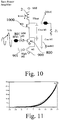
- a twin power amplifier (the same elements already discussed in figure 9 keeping the same references) which further includes a third transistor M3 1000 which has the drain and source connected in serie between the drain of transistors 800 and 900 and the output lead.
- Transistor M3 which is located on the top of the combination (cascode) is used to combine and isolate each structure from load variation ensuring better linearity.
- the output capacitance of a MOS transistor is a function of power. This capacitance is non linear and should be reduced and/or compensated. This is the goal of the output matching network.
- the Class AB contribution is low when input power is low, its capacitance will be low.
- Fig 11 gives the PAE of the pure ClassAB PA and the one using the structure. One may notice that there is almost no difference
- Fig 12 gives the linearity of the pure ClassAB PA and the one using the structure. The linearity is far better using the structure. At medium power (Pout from 10 to 16dBm) EVM is up to 10dB better. At high power, EVM is the same but mask is improved.
Landscapes
- Engineering & Computer Science (AREA)
- Power Engineering (AREA)
- Amplifiers (AREA)
Claims (7)
- Circuit amplificateur de puissance comprenant une entrée (100), une sortie (700) comprenant:- des moyens pour détecter (131, 132, 133) la tension d'entrée;- un ensemble de n circuits cascode, chacun comprenant un premier transistor (110-1, 110-2, ... 110-n) ayant une grille, une source et une borne de drain et comprenant en outre un second transistor (120-1, 120-2, ... 120-n) ayant une grille, une source et une borne de drain; la source et la grille du premier transistor desdits circuits cascode étant respectivement connectées à une première tension de référence (GND) et susceptibles de recevoir le signal d'entrée (RFin), le drain dudit premier transistor étant connecté à la source dudit second transistor dont le drain est couplé à ladite sortie (700);
caractérisé par- un circuit de commande (150) recevant la tension d'entrée détectée par lesdits moyens de détection (131, 132, 133) pour générer un ensemble de signaux de commande qui sont transmis aux grilles des seconds transistors desdits n circuits cascode;
de manière à activer ou désactiver certains desdits n circuits cascode et à adapter la taille des transistors à la puissance de sortie pour émettre en direction d'une charge. - Circuit amplificateur de puissance selon la revendication 1, caractérisé en ce que chacun desdits seconds transistors est polarisé, lorsqu'il est activé par ledit circuit de commande, dans la classe AB montrant un courant de repos Iq.
- Circuit amplificateur de puissance selon la revendication 1, caractérisé en ce que lesdits moyens de détection comprennent:- un circuit cascode supplémentaire, un premier transistor (102) ayant une grille, une source et une borne de drain et comprenant en outre un second transistor (103) ayant une grille, une source et une borne de drain; la source et la grille du premier transistor desdits circuits cascode étant respectivement connectées à une première tension de référence (GND) et susceptibles de recevoir le signal d'entrée (RFin), le drain dudit premier transistor (102) étant couplé à la source dudit second transistor (103),- un circuit passif couplé entre une tension de référence (Vdd) et le drain dudit second transistor (103) dudit circuit cascode supplémentaire, ledit circuit passif comprenant deux résistances (131, 132) montées en tant que diviseur de tension et, en parallèle, un condensateur pour calculer la moyenne du signal RF détecté par lesdits moyens de détection.
- Circuit amplificateur de puissance selon la revendication 3, caractérisé en ce que la tension de part et d'autre de l'une desdites résistances (131, 132) est transmise à une entrée dudit circuit de commande (150) pour déterminer l'amplitude du signal d'entrée à amplifier et, par conséquent, le nombre d'éléments cascode à activer/désactiver.
- Circuit amplificateur de puissance selon l'une quelconque des revendications précédentes, caractérisé en ce qu'il permet de constituer un amplificateur à radiofréquence.
- Circuit d'amplification de puissance selon l'une quelconque des revendications précédentes, caractérisé en ce qu'il est utilisé dans un téléphone portable.
- Equipement mobile comprenant un circuit d'amplification tel que défini dans l'une des revendications précédentes.
Priority Applications (4)
| Application Number | Priority Date | Filing Date | Title |
|---|---|---|---|
| EP11368002.9A EP2482449B1 (fr) | 2011-01-27 | 2011-01-27 | Circuit d'amplification avec optimisation de la puissance |
| EP19155202.5A EP3499713A1 (fr) | 2011-01-27 | 2011-01-27 | Circuit d'amplification avec optimisation de la puissance |
| PCT/EP2012/000351 WO2012100947A1 (fr) | 2011-01-27 | 2012-01-26 | Circuit d'amplification présentant une optimisation de la puissance |
| US13/996,758 US9166527B2 (en) | 2011-01-27 | 2012-01-26 | Amplification circuit having optimization of power |
Applications Claiming Priority (1)
| Application Number | Priority Date | Filing Date | Title |
|---|---|---|---|
| EP11368002.9A EP2482449B1 (fr) | 2011-01-27 | 2011-01-27 | Circuit d'amplification avec optimisation de la puissance |
Related Child Applications (2)
| Application Number | Title | Priority Date | Filing Date |
|---|---|---|---|
| EP19155202.5A Division EP3499713A1 (fr) | 2011-01-27 | 2011-01-27 | Circuit d'amplification avec optimisation de la puissance |
| EP19155202.5A Division-Into EP3499713A1 (fr) | 2011-01-27 | 2011-01-27 | Circuit d'amplification avec optimisation de la puissance |
Publications (2)
| Publication Number | Publication Date |
|---|---|
| EP2482449A1 EP2482449A1 (fr) | 2012-08-01 |
| EP2482449B1 true EP2482449B1 (fr) | 2019-03-20 |
Family
ID=44118468
Family Applications (2)
| Application Number | Title | Priority Date | Filing Date |
|---|---|---|---|
| EP19155202.5A Withdrawn EP3499713A1 (fr) | 2011-01-27 | 2011-01-27 | Circuit d'amplification avec optimisation de la puissance |
| EP11368002.9A Active EP2482449B1 (fr) | 2011-01-27 | 2011-01-27 | Circuit d'amplification avec optimisation de la puissance |
Family Applications Before (1)
| Application Number | Title | Priority Date | Filing Date |
|---|---|---|---|
| EP19155202.5A Withdrawn EP3499713A1 (fr) | 2011-01-27 | 2011-01-27 | Circuit d'amplification avec optimisation de la puissance |
Country Status (3)
| Country | Link |
|---|---|
| US (1) | US9166527B2 (fr) |
| EP (2) | EP3499713A1 (fr) |
| WO (1) | WO2012100947A1 (fr) |
Families Citing this family (6)
| Publication number | Priority date | Publication date | Assignee | Title |
|---|---|---|---|---|
| US9712125B2 (en) | 2015-02-15 | 2017-07-18 | Skyworks Solutions, Inc. | Power amplification system with shared common base biasing |
| WO2018002978A1 (fr) * | 2016-06-27 | 2018-01-04 | 三菱電機株式会社 | Amplificateur de puissance et amplificateur à gain variable |
| CN107132548B (zh) * | 2017-06-22 | 2023-07-25 | 中国人民解放军第六九O五工厂 | 一种用于北斗搜救装置的放大电路 |
| TWI706631B (zh) * | 2019-11-14 | 2020-10-01 | 財團法人工業技術研究院 | 應用於全晶片式高速通訊之低供應電壓和低消耗功率的分散式放大器 |
| CN117579007B (zh) * | 2024-01-17 | 2024-04-09 | 成都嘉纳海威科技有限责任公司 | 一种超宽带超宽动态范围放大衰减多功能芯片 |
| CN118573133B (zh) * | 2024-06-17 | 2025-04-01 | 上海芯璨电子科技有限公司 | 射频功率放大器和电子设备 |
Family Cites Families (12)
| Publication number | Priority date | Publication date | Assignee | Title |
|---|---|---|---|---|
| US4458213A (en) | 1982-12-13 | 1984-07-03 | Sony Corporation | Constant quiescent current, class AB amplifier output stage |
| US6501334B1 (en) | 2000-11-13 | 2002-12-31 | Texas Instruments Incorporated | Actively biased class AB output stage with low quiescent power, high output current drive and wide output voltage swing |
| US6448616B1 (en) * | 2001-08-14 | 2002-09-10 | Telefonaktiebolaget Lm Ericsson | Adaptive biasing of RF power transistors |
| US7088182B2 (en) | 2004-04-07 | 2006-08-08 | Texas Instruments Incorporated | Class AB output stage circuit with stable quiescent current |
| US20070270111A1 (en) * | 2006-05-19 | 2007-11-22 | Broadcom Corporation | Dual power mode transmitter |
| US7560989B2 (en) * | 2007-05-08 | 2009-07-14 | Em Microelectronic-Marin S.A. | Power amplifier with controlled output power |
| US7649411B2 (en) * | 2007-07-11 | 2010-01-19 | Axiom Microdevices, Inc. | Segmented power amplifier |
| US7839216B2 (en) * | 2008-05-27 | 2010-11-23 | Rayspan Corporation | RF power amplifiers with linearization |
| US8514015B2 (en) * | 2008-12-10 | 2013-08-20 | Qualcomm, Incorporated | Amplifier with programmable off voltage |
| US20100279641A1 (en) * | 2008-12-31 | 2010-11-04 | Siu-Chuang Ivan Lu | Receiver for wireless communication system |
| US8150343B2 (en) * | 2009-09-21 | 2012-04-03 | Broadcom Corporation | Dynamic stability, gain, efficiency and impedance control in a linear/non-linear CMOS power amplifier |
| US8188788B2 (en) * | 2010-04-23 | 2012-05-29 | Samsung Electro-Mechanics | Systems and methods for a discrete resizing of power devices with concurrent power combining structure for radio frequency power amplifier |
-
2011
- 2011-01-27 EP EP19155202.5A patent/EP3499713A1/fr not_active Withdrawn
- 2011-01-27 EP EP11368002.9A patent/EP2482449B1/fr active Active
-
2012
- 2012-01-26 WO PCT/EP2012/000351 patent/WO2012100947A1/fr not_active Ceased
- 2012-01-26 US US13/996,758 patent/US9166527B2/en not_active Expired - Fee Related
Non-Patent Citations (1)
| Title |
|---|
| None * |
Also Published As
| Publication number | Publication date |
|---|---|
| US9166527B2 (en) | 2015-10-20 |
| EP2482449A1 (fr) | 2012-08-01 |
| WO2012100947A1 (fr) | 2012-08-02 |
| US20140197893A1 (en) | 2014-07-17 |
| EP3499713A1 (fr) | 2019-06-19 |
Similar Documents
| Publication | Publication Date | Title |
|---|---|---|
| JP4792273B2 (ja) | 増幅器 | |
| EP1620942B1 (fr) | Amplificateur rf a linearisation active de charge | |
| EP2482449B1 (fr) | Circuit d'amplification avec optimisation de la puissance | |
| KR101320468B1 (ko) | 보호 회로를 갖는 캐스코드 증폭기를 위한 장치, 무선 디바이스, 및 방법 | |
| JP2006094533A (ja) | カスコード形態のクラスab制御端を備える差動増幅回路 | |
| CN101022266A (zh) | 功率放大器 | |
| JP5523619B2 (ja) | 可変利得増幅器 | |
| US20100134186A1 (en) | Low power operational amplifier | |
| US8665023B2 (en) | Class-AB/B amplifier with quiescent control circuit | |
| US20090072905A1 (en) | Variable gain amplifier having wide gain variation and wide bandwidth | |
| JP2007335942A (ja) | 可変利得増幅器 | |
| US8461926B2 (en) | Differential amplifier circuit | |
| CN102361435A (zh) | 一种可变增益宽带低噪声放大器 | |
| KR20200052696A (ko) | 낮은 위상 변화를 갖는 광대역 가변 이득 증폭기 | |
| JPWO2006006244A1 (ja) | 高出力増幅器 | |
| CN110324007B (zh) | 功率放大电路 | |
| TW201406057A (zh) | 共源共柵放大器及放大電路 | |
| KR102221543B1 (ko) | 전력 증폭 회로 | |
| JP2007259409A (ja) | 可変利得増幅器 | |
| US7368995B2 (en) | Power amplifier with active bias circuit | |
| CN201204568Y (zh) | 音频功率放大电路 | |
| JP3517777B2 (ja) | 線形高出力増幅装置 | |
| Zhang et al. | A low power programmable gain amplifier with 70-dB control range in CMOS technology | |
| KR101902381B1 (ko) | 클래스-씨 전력 증폭기를 이용한 선형 전력 증폭 회로 | |
| JP5503437B2 (ja) | 位相可変増幅器 |
Legal Events
| Date | Code | Title | Description |
|---|---|---|---|
| PUAI | Public reference made under article 153(3) epc to a published international application that has entered the european phase |
Free format text: ORIGINAL CODE: 0009012 |
|
| AK | Designated contracting states |
Kind code of ref document: A1 Designated state(s): AL AT BE BG CH CY CZ DE DK EE ES FI FR GB GR HR HU IE IS IT LI LT LU LV MC MK MT NL NO PL PT RO RS SE SI SK SM TR |
|
| AX | Request for extension of the european patent |
Extension state: BA ME |
|
| 17P | Request for examination filed |
Effective date: 20130201 |
|
| RAP1 | Party data changed (applicant data changed or rights of an application transferred) |
Owner name: OCT CIRCUIT TECHNOLOGIES INTERNATIONAL LIMITED |
|
| GRAP | Despatch of communication of intention to grant a patent |
Free format text: ORIGINAL CODE: EPIDOSNIGR1 |
|
| STAA | Information on the status of an ep patent application or granted ep patent |
Free format text: STATUS: GRANT OF PATENT IS INTENDED |
|
| INTG | Intention to grant announced |
Effective date: 20180925 |
|
| GRAS | Grant fee paid |
Free format text: ORIGINAL CODE: EPIDOSNIGR3 |
|
| GRAA | (expected) grant |
Free format text: ORIGINAL CODE: 0009210 |
|
| STAA | Information on the status of an ep patent application or granted ep patent |
Free format text: STATUS: THE PATENT HAS BEEN GRANTED |
|
| RAP1 | Party data changed (applicant data changed or rights of an application transferred) |
Owner name: TELEFONAKTIEBOLAGET LM ERICSSON (PUBL) |
|
| AK | Designated contracting states |
Kind code of ref document: B1 Designated state(s): AL AT BE BG CH CY CZ DE DK EE ES FI FR GB GR HR HU IE IS IT LI LT LU LV MC MK MT NL NO PL PT RO RS SE SI SK SM TR |
|
| REG | Reference to a national code |
Ref country code: GB Ref legal event code: FG4D |
|
| REG | Reference to a national code |
Ref country code: CH Ref legal event code: EP |
|
| REG | Reference to a national code |
Ref country code: DE Ref legal event code: R096 Ref document number: 602011057305 Country of ref document: DE |
|
| REG | Reference to a national code |
Ref country code: AT Ref legal event code: REF Ref document number: 1111550 Country of ref document: AT Kind code of ref document: T Effective date: 20190415 |
|
| REG | Reference to a national code |
Ref country code: IE Ref legal event code: FG4D |
|
| REG | Reference to a national code |
Ref country code: NL Ref legal event code: MP Effective date: 20190320 |
|
| PG25 | Lapsed in a contracting state [announced via postgrant information from national office to epo] |
Ref country code: LT Free format text: LAPSE BECAUSE OF FAILURE TO SUBMIT A TRANSLATION OF THE DESCRIPTION OR TO PAY THE FEE WITHIN THE PRESCRIBED TIME-LIMIT Effective date: 20190320 Ref country code: SE Free format text: LAPSE BECAUSE OF FAILURE TO SUBMIT A TRANSLATION OF THE DESCRIPTION OR TO PAY THE FEE WITHIN THE PRESCRIBED TIME-LIMIT Effective date: 20190320 Ref country code: FI Free format text: LAPSE BECAUSE OF FAILURE TO SUBMIT A TRANSLATION OF THE DESCRIPTION OR TO PAY THE FEE WITHIN THE PRESCRIBED TIME-LIMIT Effective date: 20190320 Ref country code: NO Free format text: LAPSE BECAUSE OF FAILURE TO SUBMIT A TRANSLATION OF THE DESCRIPTION OR TO PAY THE FEE WITHIN THE PRESCRIBED TIME-LIMIT Effective date: 20190620 |
|
| REG | Reference to a national code |
Ref country code: LT Ref legal event code: MG4D |
|
| PG25 | Lapsed in a contracting state [announced via postgrant information from national office to epo] |
Ref country code: LV Free format text: LAPSE BECAUSE OF FAILURE TO SUBMIT A TRANSLATION OF THE DESCRIPTION OR TO PAY THE FEE WITHIN THE PRESCRIBED TIME-LIMIT Effective date: 20190320 Ref country code: GR Free format text: LAPSE BECAUSE OF FAILURE TO SUBMIT A TRANSLATION OF THE DESCRIPTION OR TO PAY THE FEE WITHIN THE PRESCRIBED TIME-LIMIT Effective date: 20190621 Ref country code: HR Free format text: LAPSE BECAUSE OF FAILURE TO SUBMIT A TRANSLATION OF THE DESCRIPTION OR TO PAY THE FEE WITHIN THE PRESCRIBED TIME-LIMIT Effective date: 20190320 Ref country code: RS Free format text: LAPSE BECAUSE OF FAILURE TO SUBMIT A TRANSLATION OF THE DESCRIPTION OR TO PAY THE FEE WITHIN THE PRESCRIBED TIME-LIMIT Effective date: 20190320 Ref country code: NL Free format text: LAPSE BECAUSE OF FAILURE TO SUBMIT A TRANSLATION OF THE DESCRIPTION OR TO PAY THE FEE WITHIN THE PRESCRIBED TIME-LIMIT Effective date: 20190320 Ref country code: BG Free format text: LAPSE BECAUSE OF FAILURE TO SUBMIT A TRANSLATION OF THE DESCRIPTION OR TO PAY THE FEE WITHIN THE PRESCRIBED TIME-LIMIT Effective date: 20190620 |
|
| REG | Reference to a national code |
Ref country code: AT Ref legal event code: MK05 Ref document number: 1111550 Country of ref document: AT Kind code of ref document: T Effective date: 20190320 |
|
| PG25 | Lapsed in a contracting state [announced via postgrant information from national office to epo] |
Ref country code: ES Free format text: LAPSE BECAUSE OF FAILURE TO SUBMIT A TRANSLATION OF THE DESCRIPTION OR TO PAY THE FEE WITHIN THE PRESCRIBED TIME-LIMIT Effective date: 20190320 Ref country code: AL Free format text: LAPSE BECAUSE OF FAILURE TO SUBMIT A TRANSLATION OF THE DESCRIPTION OR TO PAY THE FEE WITHIN THE PRESCRIBED TIME-LIMIT Effective date: 20190320 Ref country code: PT Free format text: LAPSE BECAUSE OF FAILURE TO SUBMIT A TRANSLATION OF THE DESCRIPTION OR TO PAY THE FEE WITHIN THE PRESCRIBED TIME-LIMIT Effective date: 20190720 Ref country code: CZ Free format text: LAPSE BECAUSE OF FAILURE TO SUBMIT A TRANSLATION OF THE DESCRIPTION OR TO PAY THE FEE WITHIN THE PRESCRIBED TIME-LIMIT Effective date: 20190320 Ref country code: RO Free format text: LAPSE BECAUSE OF FAILURE TO SUBMIT A TRANSLATION OF THE DESCRIPTION OR TO PAY THE FEE WITHIN THE PRESCRIBED TIME-LIMIT Effective date: 20190320 Ref country code: EE Free format text: LAPSE BECAUSE OF FAILURE TO SUBMIT A TRANSLATION OF THE DESCRIPTION OR TO PAY THE FEE WITHIN THE PRESCRIBED TIME-LIMIT Effective date: 20190320 Ref country code: IT Free format text: LAPSE BECAUSE OF FAILURE TO SUBMIT A TRANSLATION OF THE DESCRIPTION OR TO PAY THE FEE WITHIN THE PRESCRIBED TIME-LIMIT Effective date: 20190320 Ref country code: SK Free format text: LAPSE BECAUSE OF FAILURE TO SUBMIT A TRANSLATION OF THE DESCRIPTION OR TO PAY THE FEE WITHIN THE PRESCRIBED TIME-LIMIT Effective date: 20190320 |
|
| PG25 | Lapsed in a contracting state [announced via postgrant information from national office to epo] |
Ref country code: PL Free format text: LAPSE BECAUSE OF FAILURE TO SUBMIT A TRANSLATION OF THE DESCRIPTION OR TO PAY THE FEE WITHIN THE PRESCRIBED TIME-LIMIT Effective date: 20190320 Ref country code: SM Free format text: LAPSE BECAUSE OF FAILURE TO SUBMIT A TRANSLATION OF THE DESCRIPTION OR TO PAY THE FEE WITHIN THE PRESCRIBED TIME-LIMIT Effective date: 20190320 |
|
| PG25 | Lapsed in a contracting state [announced via postgrant information from national office to epo] |
Ref country code: IS Free format text: LAPSE BECAUSE OF FAILURE TO SUBMIT A TRANSLATION OF THE DESCRIPTION OR TO PAY THE FEE WITHIN THE PRESCRIBED TIME-LIMIT Effective date: 20190720 Ref country code: AT Free format text: LAPSE BECAUSE OF FAILURE TO SUBMIT A TRANSLATION OF THE DESCRIPTION OR TO PAY THE FEE WITHIN THE PRESCRIBED TIME-LIMIT Effective date: 20190320 |
|
| REG | Reference to a national code |
Ref country code: DE Ref legal event code: R097 Ref document number: 602011057305 Country of ref document: DE |
|
| PLBE | No opposition filed within time limit |
Free format text: ORIGINAL CODE: 0009261 |
|
| STAA | Information on the status of an ep patent application or granted ep patent |
Free format text: STATUS: NO OPPOSITION FILED WITHIN TIME LIMIT |
|
| PG25 | Lapsed in a contracting state [announced via postgrant information from national office to epo] |
Ref country code: DK Free format text: LAPSE BECAUSE OF FAILURE TO SUBMIT A TRANSLATION OF THE DESCRIPTION OR TO PAY THE FEE WITHIN THE PRESCRIBED TIME-LIMIT Effective date: 20190320 |
|
| 26N | No opposition filed |
Effective date: 20200102 |
|
| PG25 | Lapsed in a contracting state [announced via postgrant information from national office to epo] |
Ref country code: SI Free format text: LAPSE BECAUSE OF FAILURE TO SUBMIT A TRANSLATION OF THE DESCRIPTION OR TO PAY THE FEE WITHIN THE PRESCRIBED TIME-LIMIT Effective date: 20190320 |
|
| PG25 | Lapsed in a contracting state [announced via postgrant information from national office to epo] |
Ref country code: TR Free format text: LAPSE BECAUSE OF FAILURE TO SUBMIT A TRANSLATION OF THE DESCRIPTION OR TO PAY THE FEE WITHIN THE PRESCRIBED TIME-LIMIT Effective date: 20190320 |
|
| PG25 | Lapsed in a contracting state [announced via postgrant information from national office to epo] |
Ref country code: MC Free format text: LAPSE BECAUSE OF FAILURE TO SUBMIT A TRANSLATION OF THE DESCRIPTION OR TO PAY THE FEE WITHIN THE PRESCRIBED TIME-LIMIT Effective date: 20190320 |
|
| REG | Reference to a national code |
Ref country code: CH Ref legal event code: PL |
|
| REG | Reference to a national code |
Ref country code: BE Ref legal event code: MM Effective date: 20200131 |
|
| PG25 | Lapsed in a contracting state [announced via postgrant information from national office to epo] |
Ref country code: LU Free format text: LAPSE BECAUSE OF NON-PAYMENT OF DUE FEES Effective date: 20200127 |
|
| PG25 | Lapsed in a contracting state [announced via postgrant information from national office to epo] |
Ref country code: BE Free format text: LAPSE BECAUSE OF NON-PAYMENT OF DUE FEES Effective date: 20200131 Ref country code: CH Free format text: LAPSE BECAUSE OF NON-PAYMENT OF DUE FEES Effective date: 20200131 Ref country code: LI Free format text: LAPSE BECAUSE OF NON-PAYMENT OF DUE FEES Effective date: 20200131 |
|
| PG25 | Lapsed in a contracting state [announced via postgrant information from national office to epo] |
Ref country code: IE Free format text: LAPSE BECAUSE OF NON-PAYMENT OF DUE FEES Effective date: 20200127 |
|
| PG25 | Lapsed in a contracting state [announced via postgrant information from national office to epo] |
Ref country code: MT Free format text: LAPSE BECAUSE OF FAILURE TO SUBMIT A TRANSLATION OF THE DESCRIPTION OR TO PAY THE FEE WITHIN THE PRESCRIBED TIME-LIMIT Effective date: 20190320 Ref country code: CY Free format text: LAPSE BECAUSE OF FAILURE TO SUBMIT A TRANSLATION OF THE DESCRIPTION OR TO PAY THE FEE WITHIN THE PRESCRIBED TIME-LIMIT Effective date: 20190320 |
|
| PG25 | Lapsed in a contracting state [announced via postgrant information from national office to epo] |
Ref country code: MK Free format text: LAPSE BECAUSE OF FAILURE TO SUBMIT A TRANSLATION OF THE DESCRIPTION OR TO PAY THE FEE WITHIN THE PRESCRIBED TIME-LIMIT Effective date: 20190320 |
|
| PGFP | Annual fee paid to national office [announced via postgrant information from national office to epo] |
Ref country code: FR Payment date: 20230125 Year of fee payment: 13 |
|
| PGFP | Annual fee paid to national office [announced via postgrant information from national office to epo] |
Ref country code: GB Payment date: 20230127 Year of fee payment: 13 Ref country code: DE Payment date: 20230127 Year of fee payment: 13 |
|
| P01 | Opt-out of the competence of the unified patent court (upc) registered |
Effective date: 20230523 |
|
| REG | Reference to a national code |
Ref country code: DE Ref legal event code: R119 Ref document number: 602011057305 Country of ref document: DE |
|
| GBPC | Gb: european patent ceased through non-payment of renewal fee |
Effective date: 20240127 |
|
| PG25 | Lapsed in a contracting state [announced via postgrant information from national office to epo] |
Ref country code: DE Free format text: LAPSE BECAUSE OF NON-PAYMENT OF DUE FEES Effective date: 20240801 |
|
| PG25 | Lapsed in a contracting state [announced via postgrant information from national office to epo] |
Ref country code: GB Free format text: LAPSE BECAUSE OF NON-PAYMENT OF DUE FEES Effective date: 20240127 |
|
| PG25 | Lapsed in a contracting state [announced via postgrant information from national office to epo] |
Ref country code: FR Free format text: LAPSE BECAUSE OF NON-PAYMENT OF DUE FEES Effective date: 20240131 |
|
| PG25 | Lapsed in a contracting state [announced via postgrant information from national office to epo] |
Ref country code: GB Free format text: LAPSE BECAUSE OF NON-PAYMENT OF DUE FEES Effective date: 20240127 Ref country code: FR Free format text: LAPSE BECAUSE OF NON-PAYMENT OF DUE FEES Effective date: 20240131 Ref country code: DE Free format text: LAPSE BECAUSE OF NON-PAYMENT OF DUE FEES Effective date: 20240801 |