EP2487530B1 - Panneau d'affichage comprenant un polariseur sélectif de couleur type à grille métallique - Google Patents
Panneau d'affichage comprenant un polariseur sélectif de couleur type à grille métallique Download PDFInfo
- Publication number
- EP2487530B1 EP2487530B1 EP11177489.9A EP11177489A EP2487530B1 EP 2487530 B1 EP2487530 B1 EP 2487530B1 EP 11177489 A EP11177489 A EP 11177489A EP 2487530 B1 EP2487530 B1 EP 2487530B1
- Authority
- EP
- European Patent Office
- Prior art keywords
- linear grid
- metal
- metal linear
- layer
- polarizing
- Prior art date
- Legal status (The legal status is an assumption and is not a legal conclusion. Google has not performed a legal analysis and makes no representation as to the accuracy of the status listed.)
- Not-in-force
Links
Images











Classifications
-
- G—PHYSICS
- G02—OPTICS
- G02F—OPTICAL DEVICES OR ARRANGEMENTS FOR THE CONTROL OF LIGHT BY MODIFICATION OF THE OPTICAL PROPERTIES OF THE MEDIA OF THE ELEMENTS INVOLVED THEREIN; NON-LINEAR OPTICS; FREQUENCY-CHANGING OF LIGHT; OPTICAL LOGIC ELEMENTS; OPTICAL ANALOGUE/DIGITAL CONVERTERS
- G02F1/00—Devices or arrangements for the control of the intensity, colour, phase, polarisation or direction of light arriving from an independent light source, e.g. switching, gating or modulating; Non-linear optics
- G02F1/01—Devices or arrangements for the control of the intensity, colour, phase, polarisation or direction of light arriving from an independent light source, e.g. switching, gating or modulating; Non-linear optics for the control of the intensity, phase, polarisation or colour
- G02F1/13—Devices or arrangements for the control of the intensity, colour, phase, polarisation or direction of light arriving from an independent light source, e.g. switching, gating or modulating; Non-linear optics for the control of the intensity, phase, polarisation or colour based on liquid crystals, e.g. single liquid crystal display cells
- G02F1/133—Constructional arrangements; Operation of liquid crystal cells; Circuit arrangements
- G02F1/1333—Constructional arrangements; Manufacturing methods
- G02F1/1335—Structural association of cells with optical devices, e.g. polarisers or reflectors
- G02F1/133509—Filters, e.g. light shielding masks
- G02F1/133514—Colour filters
- G02F1/133516—Methods for their manufacture, e.g. printing, electro-deposition or photolithography
-
- G—PHYSICS
- G02—OPTICS
- G02F—OPTICAL DEVICES OR ARRANGEMENTS FOR THE CONTROL OF LIGHT BY MODIFICATION OF THE OPTICAL PROPERTIES OF THE MEDIA OF THE ELEMENTS INVOLVED THEREIN; NON-LINEAR OPTICS; FREQUENCY-CHANGING OF LIGHT; OPTICAL LOGIC ELEMENTS; OPTICAL ANALOGUE/DIGITAL CONVERTERS
- G02F1/00—Devices or arrangements for the control of the intensity, colour, phase, polarisation or direction of light arriving from an independent light source, e.g. switching, gating or modulating; Non-linear optics
- G02F1/01—Devices or arrangements for the control of the intensity, colour, phase, polarisation or direction of light arriving from an independent light source, e.g. switching, gating or modulating; Non-linear optics for the control of the intensity, phase, polarisation or colour
- G02F1/13—Devices or arrangements for the control of the intensity, colour, phase, polarisation or direction of light arriving from an independent light source, e.g. switching, gating or modulating; Non-linear optics for the control of the intensity, phase, polarisation or colour based on liquid crystals, e.g. single liquid crystal display cells
- G02F1/133—Constructional arrangements; Operation of liquid crystal cells; Circuit arrangements
- G02F1/1333—Constructional arrangements; Manufacturing methods
- G02F1/1335—Structural association of cells with optical devices, e.g. polarisers or reflectors
- G02F1/133528—Polarisers
- G02F1/133533—Colour selective polarisers
-
- G—PHYSICS
- G02—OPTICS
- G02F—OPTICAL DEVICES OR ARRANGEMENTS FOR THE CONTROL OF LIGHT BY MODIFICATION OF THE OPTICAL PROPERTIES OF THE MEDIA OF THE ELEMENTS INVOLVED THEREIN; NON-LINEAR OPTICS; FREQUENCY-CHANGING OF LIGHT; OPTICAL LOGIC ELEMENTS; OPTICAL ANALOGUE/DIGITAL CONVERTERS
- G02F1/00—Devices or arrangements for the control of the intensity, colour, phase, polarisation or direction of light arriving from an independent light source, e.g. switching, gating or modulating; Non-linear optics
- G02F1/01—Devices or arrangements for the control of the intensity, colour, phase, polarisation or direction of light arriving from an independent light source, e.g. switching, gating or modulating; Non-linear optics for the control of the intensity, phase, polarisation or colour
- G02F1/13—Devices or arrangements for the control of the intensity, colour, phase, polarisation or direction of light arriving from an independent light source, e.g. switching, gating or modulating; Non-linear optics for the control of the intensity, phase, polarisation or colour based on liquid crystals, e.g. single liquid crystal display cells
- G02F1/133—Constructional arrangements; Operation of liquid crystal cells; Circuit arrangements
- G02F1/1333—Constructional arrangements; Manufacturing methods
- G02F1/1335—Structural association of cells with optical devices, e.g. polarisers or reflectors
- G02F1/133528—Polarisers
- G02F1/133548—Wire-grid polarisers
-
- G—PHYSICS
- G02—OPTICS
- G02F—OPTICAL DEVICES OR ARRANGEMENTS FOR THE CONTROL OF LIGHT BY MODIFICATION OF THE OPTICAL PROPERTIES OF THE MEDIA OF THE ELEMENTS INVOLVED THEREIN; NON-LINEAR OPTICS; FREQUENCY-CHANGING OF LIGHT; OPTICAL LOGIC ELEMENTS; OPTICAL ANALOGUE/DIGITAL CONVERTERS
- G02F2201/00—Constructional arrangements not provided for in groups G02F1/00 - G02F7/00
- G02F2201/30—Constructional arrangements not provided for in groups G02F1/00 - G02F7/00 grating
-
- G—PHYSICS
- G02—OPTICS
- G02F—OPTICAL DEVICES OR ARRANGEMENTS FOR THE CONTROL OF LIGHT BY MODIFICATION OF THE OPTICAL PROPERTIES OF THE MEDIA OF THE ELEMENTS INVOLVED THEREIN; NON-LINEAR OPTICS; FREQUENCY-CHANGING OF LIGHT; OPTICAL LOGIC ELEMENTS; OPTICAL ANALOGUE/DIGITAL CONVERTERS
- G02F2202/00—Materials and properties
- G02F2202/36—Micro- or nanomaterials
-
- G—PHYSICS
- G02—OPTICS
- G02F—OPTICAL DEVICES OR ARRANGEMENTS FOR THE CONTROL OF LIGHT BY MODIFICATION OF THE OPTICAL PROPERTIES OF THE MEDIA OF THE ELEMENTS INVOLVED THEREIN; NON-LINEAR OPTICS; FREQUENCY-CHANGING OF LIGHT; OPTICAL LOGIC ELEMENTS; OPTICAL ANALOGUE/DIGITAL CONVERTERS
- G02F2203/00—Function characteristic
- G02F2203/10—Function characteristic plasmon
Definitions
- Apparatuses and methods consistent with the exemplary embodiments relate to a display panel and a display apparatus including the same, and more particularly, to a display panel including a color filter polarizing layer and a polarizing layer and a display apparatus including the same.
- a liquid crystal display (LCD) panel includes first and second substrates having a liquid crystal layer therebetween, and a polarizing film for polarizing light incident to the first and second substrates. Also, the LCD panel includes a color filter layer to create different colors with the incident light. While the incident light passes through the polarizing film and the color filter layer, its optical efficiency becomes lowered. Meanwhile, the LCD panel may further include a dual brightness enhance film (DBEF) at a light-incident side so as to compensate for light loss due to polarization.
- DBEF dual brightness enhance film
- the polarizing film and the DBEF increase manufacturing costs of the LCD panel or the display apparatus and make a manufacturing process complicated.
- US 2008/0100781 A1 describes a liquid crystal display and a method of manufacturing the same.
- a wire grid polarizing pattern is formed on at least one of thin film transistor and color filter substrates in a manufacturing process thereof.
- US 2007/0019292 A1 describes a hybrid-type polarizer having a reflective-type polarizing filter and a color filter, a method of manufacturing the hybrid-type polarizer and a display device having the hybrid-type polarizer, and hybrid-type polarizer includes a base member and a polarizing color filter member.
- the polarizing color filter member includes a plurality of metal gratings in a plurality of regions of the base member.
- one or more exemplary embodiments provide a display panel which may be used in a display apparatus and in which manufacturing costs are decreased and a manufacturing process is simplified.
- a display panel having improved optical efficiency and a display apparatus including the same According to an aspect of an exemplary embodiment, there is provided a display panel having improved optical efficiency and a display apparatus including the same.
- the display apparatus has a passive type stereoscopic image excellent in visibility.
- a display panel with a liquid crystal layer, including first and second substrates which are disposed opposite to each other; a color filter polarizing layer which is formed on one surface between the first and second substrates, and includes a first metal linear grid arranged at different pitches to filter different colors a first polarized component of incident light; and a polarizing layer which includes a second metal linear grid formed on an opposing surface to the one surface between the first and second substrates, wherein a metal contained in the first metal linear grid has different properties from a metal contained in the second metal linear grid.
- the first metal linear grid has a higher reflectivity than the second metal linear grid, and the second metal linear grid has a higher strength to absorb external impacts than the first metal linear grid
- the metal contained in the first metal linear grid may be different in material from the metal contained in the second metal linear grid.
- One of the first substrate and the second substrate may further include a light absorbing layer formed on the metal linear grid arranged to absorb light.
- One of the first substrate and the second substrate may further include a light absorbing layer formed beneath the metal linear grid arranged to absorb light.
- the display panel may further include a pixel layer formed on one surface between the first substrate and the second substrate and formed with a pixel including a plurality of sub pixels, wherein at least three sub pixels are different in the pitch of the first metal linear grid.
- the first metal linear grid may include a red metal linear grid, a green metal linear grid and a blue metal linear grid, and the red metal linear grid has every pitch shorter than 1/2 of a red light wavelength, the green metal linear grid has every pitch shorter than 1/2 of a green light wavelength, and the blue metal linear grid has every pitch shorter than 1/2 of a blue light wavelength.
- the first metal linear grid may include a first metal layer, an insulating layer, and a second metal layer stacked in sequence.
- the height of the first metal linear grid may be larger than the width thereof.
- the color filter polarizing layer may further include a dielectric layer stacked beneath the first metal linear grid.
- the display panel can be used in a display apparatus with a liquid crystal layer, including a backlight assembly which emits light to the display panel.
- a method of manufacturing a display apparatus is defined in claim 10 and comrpises amongst others the following steps forming a color filter polarizing layer, including a first polarizing linear grid transmitting a first polarizing component and a second polarizing linear grid transmitting a second polarizing component in form of a checkerboard, on a surface of a first substrate located between the first substrate and a second substrate; forming a polarizing layer, including a first polarizing linear grid transmitting a first polarizing component and a second polarizing linear grid transmitting a second polarizing component in form of a checkerboard, on a surface of the second substrate located between the first and second substrates; forming a pixel layer including a plurality of sub pixels on one of the color filter polarizing layer or the polarizing layer; and encapsulating the first and second substrates and injecting a liquid crystal in a space formed between the first and second substrates.
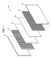
- FIG. 1 shows a basic layer structure of a display panel used in exemplary embodiments of the present invention
- FIG. 2 is a cross-section view of a display panel of FIG. 1 .
- a display panel 1000 in this exemplary embodiment includes first and second substrates 100 and 200 opposite to each other, and a color filter polarizing layer 300, a pixel layer 400 and a liquid crystal layer 500 and a polarizing layer 600 arranged in sequence between the first and second substrates 100 and 200.
- the display panel 1000 including the liquid crystal layer 500 may be used in a television, home appliances such as a monitor, a cellular phone, a portable multimedia player (PMP), a Netbook, a notebook computer, a mobile terminal such as an E-book terminal or the like, a display apparatus for exhibition and advertisement, etc.
- the color filter polarizing layer 300 and the pixel layer 400 are formed in sequence on the first substrate 100, and a polarizing layer 600 is formed on the second substrate 200.
- the second substrate 200 is formed with a black matrix 200-1 in a region corresponding to the TFT 411 of the first substrate 100, and a common electrode 200-3 generating a voltage corresponding to the pixel electrode 412.
- the liquid crystal layer 500 of which alignment is adjusted by applied voltage, is inserted between the first and second substrates 100 and 200.
- the array of the liquid crystal layer 500 is controlled in accordance with a twisted nematic (TN) mode, a vertical alignment (VA) mode, a patterned vertical alignment (PVA) mode, an in-plane switching (IPS) mode or the like operating mode of the display panel 1000.
- TN twisted nematic
- VA vertical alignment
- PVA patterned vertical alignment
- IPS in-plane switching
- sub pixels are divided or patterned, the refractive index of the liquid crystal is uniformly adjusted, or the like technology may be used.
- the color filter polarizing layer 300 is formed on the first substrate 100, and the pixel layer 400 for controlling the liquid crystal array and displaying an image is formed on the color filter polarizing layer 300.
- the color filter polarizing layer 300 includes the first metal linear grid 310 arranged with different pitches so that first polarized component of the incident light can be filtered -or in the following also called "emitted"- as light of different color.
- the polarizing layer 600 may include a second metal linear grid 610 that transmits light of a second polarized component different from the first polarized component, and changes only a polarized state of the incident light.
- a planarization layer 100-1 is formed for protecting and leveling them.
- the first metal linear grid 310 included in the color filter polarizing layer 300 and the second metal linear grid 610 included in the polarizing layer 600 will be described below in detail.
- the pixel layer 400 formed on the planarization layer 100-1 includes a plurality of pixels (not shown) for changing the liquid crystal array filled in the liquid crystal layer 500 based on a control signal received from the exterior, and each pixel includes a plurality of sub pixels 410.
- the sub pixels 410 represent the smallest unit pixel in which video signal values corresponding to red, green and blue are input, and a unit, which includes a plurality of sub pixels 410 and expresses one video signal, is regarded as the pixel.
- the sub pixel 410 includes a thin film transistor (TFT) 411 as a switching device, and a pixel electrode 412.
- TFT thin film transistor
- the sub pixel 410 has a two-dimensional spatial concept as well as a physical concept including the TFT 411 and the pixel electrode 412.
- the gate electrode 411-1 On the planarization layer 100-1 of the first substrate 100, the gate electrode 411-1 is formed.
- the gate electrode 411-1 may be a single or multiple layers containing metal.
- On the same layer as the gate electrode 411-1 there are further formed a gate line (not shown) connected to the gate electrode and arranged in a transverse direction of the display panel 1000, and a gate pad (not shown) connected to a gate driver (not shown) and transmitting a driving signal to the gate line.
- a sustain electrode 413 is formed for building up electric charges.
- a gate insulating layer 411-2 containing silicon nitride (SiNx) or the like covers the gate electrode 411-1 and the sustain electrode 413.
- a semiconductor layer 411-3 containing amorphous silicon or the like semiconductor is formed on the gate insulating layer 411-2 of the gate electrode 411-1.
- a semiconductor layer 411-3 containing amorphous silicon or the like semiconductor is formed on the semiconductor layer 411-3.
- an ohmic contact layer 411-4 containing n+ hydrogenated amorphous silicon or the like material highly doped with silicide or n-type impurities is formed on the semiconductor layer 411-3. Further, the ohmic contact layer 411-4 is removed in a channel portion between a source electrode 411-5 and a drain electrode 411-6 to be described later.
- the data wiring lines 411-5 and 411-6 are formed on the ohmic contact layer 411-4 and the gate insulating layer 411-2.
- the data wiring lines 411-5 and 411-6 may also be a single or multiple layers containing metal.
- the data wiring lines 411-5 and 411-6 includes a data line (not shown) formed in a vertical direction and intersecting a gate line (not shown) to form the sub pixel 410, a source electrode 411-5 branched from the data line and extended to an upper portion of the ohmic contact layer 411-4, and a drain electrode 411-6 separated from the source electrode 411-5 and formed on an upper portion of the ohmic contact layer 411-4 opposite to the source electrode 411-5.
- a passivation layer 411-7 is formed on the data wiring lines 411-5 and 411-6 and the semiconductor layer 411-3 that is not covered with the data wiring lines 411-5 and 411-6. At this time, silicon nitride or the like inorganic insulting film may be further formed between the passivation layer 411-7 and the TFT 411, thereby securing the reliability of the TFT 411.
- the pixel electrode 412 formed on the passivation layer 411-7 contains indium tin oxide (ITO) or indium zinc oxide (IZO), or the like transparent conductive material.
- ITO indium tin oxide
- IZO indium zinc oxide
- the pixel electrode 412 is electrically connected to the source electrode 411-5.
- the black matrix 200-1 is formed in a region corresponding to the TFT 411 of the first substrate 100.
- the black matrix 200-1 serves to divide the sub pixels 410 and prevent the TFT 411 from being exposed to external light.
- the black matrix 200-1 contains a photosensitive organic material with black dye.
- the black dye carbon black, titanium oxide or the like is used.
- an overcoat layer 200-2 is formed for leveling and protecting the black matrix 200-1.
- an acrylic epoxy material is typically used.
- a common electrode 200-3 is formed on the overcoat layer 200-2.
- the common electrode 200-3 is made of a transparent conductive material such as indium tin oxide (ITO), indium zinc oxide (IZO), etc.
- ITO indium tin oxide
- IZO indium zinc oxide
- FIG. 3 is a view showing a color filter polarizing layer on a first substrate of FIG. 1
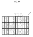
- FIGS. 4A and 4B are views for explaining a first metal linear grid of a sub pixel
- FIG. 5 is a cross-section view of the color filter polarizing layer of FIG. 3 .
- the first metal linear grid 310 is shaped like a bar arranged in certain direction on the first substrate 100.
- the first metal linear grid 310 is periodically arranged with certain height (H) and width (W).
- the cycle, i.e., the pitch of the first metal linear grid 310 is arranged or formed differently according to desired colors of light.
- a pitch of a diffraction grid is adjusted to be equal to or shorter than 1/2 of the wavelength of the light, a diffraction wave is not formed but only transmitted light and reflected light exist.
- the first metal linear grid 310 shaped like a slit
- the first polarized component of the incident light which is perpendicular to the first metal linear grid 310
- a second polarized component which is perpendicular to the first metal linear grid 310
- FIG. 4A is a view showing a pixel I and sub pixels 410-R, 410-G and 410-B constituting the pixel I.
- the pixel I includes a red sub pixel 410-R formed in a region where red light is emitted, a green sub pixel 410-G formed in a region where green light is emitted, and a blue sub pixel 410-B formed in a region where blue light is emitted.
- the color filter polarizing layer 300 corresponding to such a pixel layer 400 is formed with the first metal linear grid 310 having different pitches according to the sub pixels 410-R, 410-G and 410-B.
- FIG. 4B is a view showing the first metal linear grid 310 corresponding to the sub pixels 410-R, 410-G and 410-B.
- the first metal linear grid 310 includes a red metal linear grid 310-R formed in a region corresponding to the red sub pixel 410-R, a green metal linear grid 310-G formed in a region corresponding to the green sub pixel 410-G, and a blue metal linear grid 310-B formed in a region corresponding to the blue sub pixel 410-B.
- the red metal linear grid 310-R is arranged such that every pitch is shorter than 1/2 of a red light wavelength
- the green metal linear grid 310-G is arranged such that every pitch is shorter than 1/2 of a green light wavelength
- the blue metal linear grid 310-B is arranged such that every pitch is shorter than 1/2 of a blue light wavelength.
- the pitch of the red metal linear grid 310-R is shorter than 1/2 of the red light wavelength, i.e., about 330 - 390nm, and the incident light is separated into a red light spectrum having a first polarized component while passing through the red metal linear grid 310-R.
- the pitch of the green metal linear grid 310-G is shorter than 1/2 of the green light wavelength, i.e., about 250 - 290nm, and the incident light is separated into a green light spectrum having the first polarized component.
- the pitch of the blue metal linear grid 310-B may be set up to be shorter than 1/2 of the blue light wavelength, i.e., about 220 - 240nm.
- the light passing through the blue metal linear grid 310-B is separated into a blue light spectrum having the first polarized component.
- the pitches of the metal linear grid 310 are decreased in order of the red metal linear grid 310-R, the green metal linear grid 310-G and the blue metal linear grid 310-B.
- the pitch of the first metal linear grid 310 may be adjusted in accordance with light wavelengths of color desired to be emitted from the display panel 1000, and light of yellow, cyan and magenta may be emitted instead of the foregoing light of red, green and blue.
- the first metal linear grid 310 includes a first metal layer 311, an insulating layer 313 and a second metal layer 315 sequentially stacked.
- the first metal layer 311 and the second metal layer 315 may be made of metal such as Al, Ag, etc. and may have a height of less than about 100nm.
- each of the first metal layer 311 and the second metal layer 315 may be formed to have a height of about 40nm.
- the insulating layer 313 stacked between the first metal layer 311 and the second metal layer 315 may include a dielectric material such as ZnSe and TiO2, and may be formed to have a height of less than about 150nm.
- the height of the first metal linear grid 310 is larger than the width thereof, and a ratio of height to width may be 2 - 4, for example, 3.
- the width, the height, the pitch, the ratio of height to width, and a ratio of pitch to width may be varied depending on the material forming the first metal linear grid 310. That is, simulation about optical transmittance is conducted by taking the kind of metal, the height of dielectric material, etc. into account, and an optimal condition may be selected.
- the width, the height, the pitch, the ratio of height to width, and a ratio of pitch to width of the first metal linear grid 310 may be varied depending on color of emitted light, i.e., each sub pixel 410.
- the principle that colored light is emitted from the metal layer 311, 315 of the first metal linear grid 310 is based on Plasmon in which free electrons in metal are collectively oscillated.
- Nano-sized metal shows Plasmon resonance on a surface of the metal due to the oscillation of the free electrons.
- the surface Plasmon resonance is collective charge density oscillation of the electrons on the surface of a metal thin film, and a surface Plasmon wave caused by the surface Plasmon resonance is a surface electromagnetic wave propagating along a boundary surface between the metal and the dielectric material adjacent to the metal.
- the surface Plasmon wave corresponds to a wave generated when light incident to the metal surface and having a certain wavelength is not totally reflected and causes a surface wave. If the metal linear grid 310 including the first metal layer 311, the insulating layer 313 and the second metal layer 315 is arranged in the form of slits in a certain cycle, the color of emitted light is varied depending on the cycle.
- the first metal linear grid 310 is configured to make white light filter into individual colors throughout a visible light region. This is to achieve a nano oscillator for quantum-Plasmon-quantum conversion within a certain oscillation wavelength, when enhances a pass bandwidth and makes compactness possible as compared with other color filtering methods. Also, the filtered light has already been naturally polarized, so that it can be directly applied to an LCD panel or the like without any separate polarizing layer.
- the display panel 100 can generate polarized colored light through one color filter polarizing layer 300 instead of the existing polarizing film and color filter. Also, light that is not transmitted through the first substrate 100 is not absorbed but is instead reflected from the first metal layer 311 of the first metal linear grid 310, so that it is likely to be reflected again toward the display panel 1000. That is, the total optical efficiency is improved so that the conventional dual brightness enhance film (DBEF) can be omitted.
- DBEF dual brightness enhance film
- FIG. 6 is a cross-section view of the polarizing layer on the second substrate of FIG. 1 .
- the polarizing layer 600 includes the second metal linear grid 610 shaped like a bar arranged in a direction perpendicular to the first metal linear grid 310. That is, the second metal linear grid 610 transmits a second polarized component perpendicular to the first polarized component.
- the second metal linear grid 610 has a pitch capable of transmitting incident light of all wavelengths since it has only to transmit the second polarized component. Particularly, the pitch of the second metal linear grid 610 may be formed to be shorter than 1/2 of a blue light wavelength.
- the second metal linear grid 610 has a height of about 150nm and a pitch of 100 to 150nm. Also, a ratio of height to width of the second metal linear grid 610 may be adjusted within a range from 2 to 4.
- the second metal linear grid 610 includes a metal layer 611 and a hard mask 612 formed on the metal layer 611.
- the metal layer 611 may contain the same metal as or a different metal from that of the first metal linear grid 310.
- the metal layer 611 may contain metal such as Al, Ag, Cu, etc., or may contain MoW or the like hard alloy.
- the metal layer 611 may be made of a conductive polymer or may contain the conductive polymer.
- the hard mask 612 serves to protect the metal layer 611 and improve polarizing performance of the metal layer 611, and may contain a dielectric material such as Si02.
- the first metal linear grid 310 and the second metal linear grid 610 may have the same polarizing direction. Since it can be set up such that the light is blocked out or transmitted in accordance with whether a voltage is applied or not by adjusting the state of the liquid crystal depending on an orientation, there is no need for making the polarizing directions of the first metal linear grid 310 and the second metal linear grid 610 be perpendicular to each other. This may be adjusted in accordance with the orientation of the liquid crystal.
- FIGS. 7 to 9 are views showing a color filter polarizing layer and a polarizing layer of a display panel according to an embodiment of the present invention.
- the display panel 1000 of FIGs. 7 to 9 includes the first metal linear grid 310 and the second metal linear grid 610 different from each other in material, particularly, in metal material contained therein.
- the metal contained in the first metal linear grid 310 and the second metal linear grid 610 are different from each other in reflectivity or hardness.
- the display panel 1000 of FIG. 7 includes the first metal linear grid 310 containing metal of high reflectivity, and a second metal linear grid 610 containing metal of low reflectivity. If light enters through the bottom of the first substrate 100 and exits through the second substrate 200, the light of only the first polarized component enters the liquid crystal layer 500, and the light of the second polarized component is reflected from the first substrate 100.
- a backlight assembly (not shown) emitting light under the display panel 1000 includes a reflective plate that reflects light reflected from the first substrate 100 toward the display panel 1000 again.
- Metal contained in the first metal linear grid 310 has a high reflectivity so that more light can be recycled by the reflective plate and enter the first substrate 100, i.e., much more light of the second polarized component can enter the reflective plate.
- the first metal linear grid 310 may include a metal having high reflectivity, such as Al, Ag, Cu, etc.
- DBEF dual brightness enhance film
- the second metal linear grid 610 may contain metal having low reflectivity so as to suppress reflection of external light and absorb the light.
- the second metal linear grid 610 may undergo additional processes for decreasing the reflectivity of the metal, or may include or be configured with carbon, chrome oxide, etc. for absorbing the light.
- the second metal linear grid 610 includes metal having high strength such as to absorb external impacts.
- the second metal linear grid 610 may contain MoW or the like alloy, or may contain conductive polymer capable of performing substantially the same function as the metal layer.
- the display panel 1000 of FIG. 8 may further include a light absorbing layer 330 formed on the first metal linear grid 310 included in the first substrate 100 and absorbing light. If external light enters the display panel 1000 and is reflected again, there are problems that a contrast ratio of the display panel 1000 may be lowered and picture quality may be deteriorated due to the reflection of light. To prevent these problems, the first substrate 100 according to this exemplary embodiment includes the light absorbing layer 330 on the first metal linear grid 310 in order to absorb undesired external light.
- the light absorbing layer 330 may contain metal having low reflectivity, and or may include or be configured with carbon, chrome oxide, etc. for absorbing the light.
- the light absorbing layer 330 may be formed not on the first substrate but beneath the second metal linear grid 610 of the second substrate 200. That is, the external light is intercepted by the light absorbing layer formed beneath the second metal linear grid 610 and thus prevented from entering the display panel 1000.
- FIG. 9 shows a first light absorbing layer 331 formed on the first metal linear grid 310 of the first substrate 100 and a second light absorbing layer 631 formed on the second substrate 200.
- the display panel 1000 includes the light absorbing layers 331 and 631 disposed on both the first and second substrates 100 and 200.
- the light absorbing layers 331 and 631 may be configured with carbon, chrome oxide, etc.
- the first light absorbing layer 331 and the second light absorbing layer 631 may be formed on either of the substrates as shown in FIG. 8 , or may be omitted.
- FIG. 10 is a cross-section view of another color filter polarizing layer according to an exemplary embodiment.
- the color filter polarizing layer 300 may further include a dielectric layer 320 stacked under the first metal linear grid 310.
- the dielectric layer 320 may be made of a material similar to the first substrate 100, and may contain MgF2.
- the dielectric layer 320 may be provided in the form of a film coupled to the first substrate 100.
- the dielectric layer 320 may replace the first substrate 100 or may be omitted.
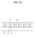
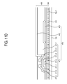
- FIGS. 11A to 11D are views for explaining a manufacturing method for a first substrate of a display panel according to still another exemplary embodiment.
- the first metal layer 311, the insulating layer 313 and the second metal layer 315 are stacked in sequence by a sputtering method or the like in order to form a color filter polarizing layer 300 on the first substrate 100.
- a general patterning process is performed.
- photoresist is deposited, exposed to light through a mask, and developed and etched to thereby form the first metal linear grid 310. That is, in this exemplary embodiment, the first metal layer 311, the insulating layer 313 and the second metal layer 315 are not respectively formed but stacked in sequence and once patterned to form the first metal linear grid 310.
- the process of forming the first metal linear grid 310 may be achieved by any publicly-known or not-known patterning technique.
- the planarization layer 100-1 is formed for protecting and leveling the surface of the first metal linear grid 310.
- the planarization layer 100-1 may contain silicon nitride SiNx.
- the TFT 411 and the pixel electrode 412 electrically connected to the TFT 411 are formed on the planarization layer 100-1.
- the pixel electrode 412 may be formed by depositing metal by the sputtering method and patterning it (refer to FIG. 11 D) .
- FIG. 12A to 12D are views for explaining a manufacturing method for a second substrate of a display panel according to still another exemplary embodiment.
- the polarizing layer 600 of the second substrate 200 may be formed by a method similar to that for the color filter polarizing layer 300 of the first substrate 100. That is, as shown in FIG. 12A , the metal layer 611 and the hard mask 612 for protecting the metal layer 611 are stacked on the second substrate 200.
- the second metal linear grid 610 is formed by performing a photolithography or etching process once.
- the planarization layer 100-1 for protecting and leveling the surface of the second metal linear grid 610 is formed.
- the black matrix 200-1 is formed on the planarization layer 100-1 in a region corresponding to the TFT 141, and the overcoat layer 200-2 is formed for leveling the black matrix 200-1. Further, the common electrode 200-3 containing a transparent conductive material is formed by a sputtering method.
- the two substrates 100 and 200 of FIGS. 12D and 11D are coupled and encapsulated with each other, and the liquid crystal is inserted therein, thereby completing the display panel 1000.
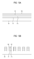
- FIG. 13A and 13B are views for explaining a forming method for a light absorbing layer according to an exemplary embodiment.
- FIG. 13A shows that the first metal layer 311, the insulating layer 313, the second metal layer 315, and the light absorbing layer 330 are sequentially stacked on the first substrate.
- a patterning process is applied once to form the first metal linear grid 310 and the light absorbing layer 330.
- FIG. 14A and 14B are views for explaining a forming method for a light absorbing layer according to another exemplary embodiment.
- the light absorbing layer 330 is formed beneath the second metal linear grid 610. As shown in FIG. 14A , the light absorbing layer 330, the metal layer 611 and a hard mask 612 are sequentially stacked on the second substrate 200.
- a patterning process is applied once to form the second metal linear grid 610 and the light absorbing layer 330.
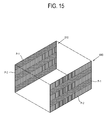
- FIG. 15 is a view for explaining polarization of first and second metal linear grids of the display panel according to an exemplary embodiment.
- the line shown in FIG. 15 schematically illustrates orientation of the first metal linear grid 310 formed on the color filter polarizing layer 300 and the second metal linear grid 610 formed on the polarizing layer 600.
- the polarized components of the transmitted light are different. For example, if a horizontal line transmits the first polarized component of the light, a vertical line transmits the second polarized component.
- the display panel 1000 according to this exemplary embodiment is useful to a display apparatus that displays a three-dimensional (3D) image, particularly, to a display apparatus that displays a 3D image in a passive mode. In the case of displaying the 3D image by the passive mode, a user can view an image through polarization glasses having different polarized states.
- the color filter polarizing layer 300 is divided into a plurality of rows, and the first metal linear grid 310 includes a fist polarizing linear grid P-1 for transmitting the first polarized component and a second polarizing linear grid P-2 for transmitting the second polarized component.
- the first polarizing linear grid P-1 is formed in odd-numbered rows and the second polarizing linear grid P-2 is formed in even-numbered rows, which are alternate to each other.
- the second metal linear grid 610 includes the first polarizing linear grid P-1 for transmitting the first polarized component and the second polarizing linear grid P-2 for transmitting the second polarized component.
- the first polarizing linear grid P-1 of the second metal linear grid 610 is formed in even-numbered rows and the second polarizing linear grid P-2 is formed in odd-numbered rows, which alternate to each other.
- first polarizing linear grid P-1 of the second metal linear grid 610 is formed to correspond to the second polarizing linear grid P-2 of the first metal linear grid 310
- second polarizing linear grid P-2 of the second metal linear grid 610 is formed to correspond to the first polarizing linear grid P-1 of the first metal linear grid 310, which alternate to each other.
- the left-eye image is displayed on the display panel 1000 through the first polarizing linear grid P-1 of the first metal linear grid 310 and the second polarizing linear grid P-2 of the second metal linear grid 610
- the right-eye image is displayed on the display panel 1000 through the second polarizing linear grid P-2 of the first metal linear grid 310 and the first polarizing linear grid P-1 of the second metal linear grid 610.
- the left-eye image and the right-eye image are simultaneously displayed on the display panel 1000, a user's two eyes respectively view different images through the polarization glasses that can transmit only one polarized component of the left-eye and right-eye images, thereby viewing the 3D image.
- the repeated cycle of the first polarizing linear grid P-1 and the second polarizing linear grid P-2 may be based on one pixel row or a plurality of pixel rows.
- the color filter polarizing layer 300 may be divided into a plurality of columns, and the first polarizing linear grid P-1 and the second polarizing linear grid P-2 may be alternately formed at every column.
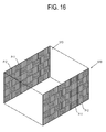
- FIG. 16 is a view for explaining polarization of first and second metal linear grids of the display panel according to another exemplary embodiment.
- the color filter polarizing layer 300 in this exemplary embodiment is divided in form of a checkerboard, and the first polarizing linear grid P-1 and the second polarizing linear grid P-2 are alternately formed in adjacent cells on the checkerboard.
- the first polarizing linear grid P-1 of the first metal linear grid 310 corresponds to the second polarizing linear grid P-2 of the second metal linear grid 610
- the second polarizing linear grid P-2 of the first metal linear grid 310 corresponds to the first polarizing linear grid P-1 of the second metal linear grid 610.
- the left-eye image and the right-eye image may be alternately displayed in the adjacent cells of the checker board, and a user can view the 3D image through the same polarization glasses as those of the foregoing exemplary embodiment.
- an image having resolution substantially lower than that of the display panel 1000 is displayed, but the left-eye image and the right-eye image are repeated in a grid pattern so that a user cannot sense decrease in the resolution. That is, a user can view an image having higher resolution than that of the exemplary embodiment shown in FIG. 15 .
- the cells of the checkerboard may correspond to individual pixels of the pixel layer 400, and may correspond to a plurality of pixels.
- the display panel 1000 of FIGS. 15 and 16 may externally include a polarizer for changing linearly polarized light transmitted through the polarizing layer 600 into circularly polarized light. To secure a viewing angle and enable a user to view a 3D image even though a user views it in any direction, the display panel 1000 may emit the circularly polarized light.
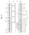
- FIG. 17 is a cross-sectional view of a display panel according to another exemplary embodiment.
- the display panel 1000 in this exemplary embodiment further includes an additional polarizing layer 800 beneath the color filter polarizing layer 300 to transmit the first polarizing component.
- the additional polarizing layer 800 may further include a third metal linear grid 810 that contains substantially the same metal as the metal contained in the second metal linear grid 610 and is arranged in the same direction as the first metal linear grid 310.
- the third metal linear grid 810 is arranged in the same direction as the first metal linear grid 310, and thus transmits the first polarized component.
- the light of the first polarized component passed through the additional polarizing layer 800 is emitted with red, blue and green colors while passing through the color filter polarizing layer 300.
- the metal layer contained in the third metal linear grid 810 may contain highly-reflective metal, e.g., at least one of Al, Ag and Cu. Further, a light absorbing layer may be further provided on the metal layer and absorb external light.
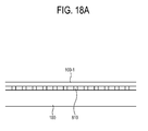
- FIG. 18A and 18B are views for explaining a forming method for an additional polarizing layer according to an exemplary embodiment.
- the additional polarizing layer 800 including the third metal linear grid 810 is formed on the first substrate 100, and the polarization layer 100-1 is formed on the additional polarizing layer 800.
- the color filter polarizing layer 300 and the pixel layer 400 are sequentially formed. If the second substrate 200 is formed as shown in FIG. 12D and then combined to FIG. 18B , the display panel 1000 including the additional polarizing layer 800, the color filter polarizing layer 300 and the polarizing layer 600 is completed.
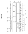
- FIG. 19 is a cross-section view of a display panel according to still another exemplary embodiment.
- the display panel 1000 includes a polarizing layer 600 formed on the first substrate 100, and a color filter polarizing layer 300 formed on the second substrate 200.
- the color filter polarizing layer 300 may be arranged on not the pixel layer 400 but the substrate formed with the black matrix 200-1. If light enters through the bottom of the first substrate 100, the light of second polarized component passed through the polarizing layer 600 passes through the liquid crystal layer 500, and is then emitted as the light of the first polarized component with different colors while passing through the color filter polarizing layer 300.
- Each of the color filter polarizing layer 300 and the polarizing layer 600 may be selectively formed on the same or different substrates as the pixel electrode 400. Of course, light may enter though the second substrate 200 and exit through the first substrate 100.
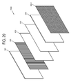
- FIG. 20 is a view showing a layer structure of a display panel according to still another exemplary embodiment
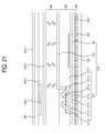
- FIG. 21 is a cross-section view of the display panel of FIG. 20 .
- the display panel 1000 in this exemplary embodiment includes first and second substrates 100 and 200 disposed opposite to each other; a color filter polarizing layer 300, the pixel layer 400 and the liquid crystal layer 500 sequentially arranged between the first and second substrates; and a polarizing film 600-1 arranged on an outside surface of the second substrate 200.
- the polarizing film 600-1 transmits light of a second polarized component different from the first polarized component, and replaces the polarizing layer 600 included in the foregoing exemplary embodiment.
- the polarizing film 600-1 may be attached to the outside surface of the first substrate 100, and the color filter polarizing layer 300 may be formed on the second substrate 200.
- the color filter polarizing layer 300 may be arranged on not the pixel layer 400 but the substrate formed with the black matrix 200-1. If light enters through the bottom of the first substrate 100, the light of second polarized component passed through the polarizing film 600-1 passes through the liquid crystal layer 500, and then exits as the light of the first polarized component with different colors while passing through the color filter polarizing layer 300.
- Each of the color filter polarizing layer 300 and the polarizing film 600-1 may be selectively formed on the same or different substrates as the pixel electrode 400. Of course, light may enter though the second substrate 200 and exit through the first substrate 100.
- FIG. 22 is a cross-section view showing an exemplary embodiment of the color filter polarizing layer of FIG. 20 .
- the display panel 1000 may further include a light absorbing layer 330 formed on the first metal linear grid 310 included in the first substrate 100 and absorbing light. If external light enters the display panel 1000 and is reflected again, there are problems that a contrast ratio of the display panel 1000 may be lowered and picture quality may be deteriorated due to the reflection of light.
- the first substrate 100 includes the light absorbing layer 330 on the first metal linear grid 310 in order to absorb undesired external light.
- the light absorbing layer 330 may contain metal having low reflectivity, and or may include or be configured with carbon, chrome oxide, etc. for absorbing the light.
- FIG. 23 is a cross-section view showing another exemplary embodiment of the color filter polarizing layer of FIG. 20 .
- a light absorbing layer 330-1 may be formed on not the first substrate 100 but the second substrate 200. That is, incident light from the exterior is intercepted by the light absorbing layer 330-1 and prevented from entering the display panel 1000.
- the light absorbing layer 330, 330-1 may be selectively formed on one of the first substrate 100 and the second substrate 200 in accordance with whether the light enters the first substrate 100 or the second substrate 200 of the display panel 1000.
- the color filter polarizing layer 300 may further include a dielectric layer (not shown) stacked under the first metal linear grid 311.
- the dielectric layer may be made of a material similar to the first substrate 100, and may contain MgF2.
- the dielectric layer may be provided in the form of a film coupled to the first substrate 100, and the dielectric layer may replace the first substrate 100 or be omitted.
- the dielectric layer 320 may replace the first substrate 100 or may be omitted.
- the display panel 1000 may further include a printed circuit board mounted with a gate driving integrated chip (IC) and a data chip film package, which are not shown. Also, a compensation film (not shown) may be further provided outside the first substrate 100 and the second substrate 200.
- IC gate driving integrated chip
- a compensation film (not shown) may be further provided outside the first substrate 100 and the second substrate 200.
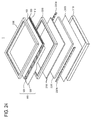
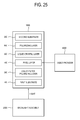
- FIG. 24 is a schematic view of a display apparatus and FIG. 25 is a control block diagram of a display apparatus in which the displaay panel according to the present invention can be used.
- the display apparatus 1 includes the display panel 1000, the backlight assembly 2000, accommodating containers 3100, 3200, 3300 accommodating them, and a video provider 4000.
- the display panel 1000 includes the first substrate 100, the second substrate 200 opposite to the first substrate 100, the liquid crystal layer (not shown) interposed between the first substrate 100 and the second substrate 200, and a panel driver 900 for driving the pixel layer 400 to display a video signal.
- the panel driver 900 may include a gate driving IC 910, a data chip film package 920, and a printed circuit board 930.
- the first substrate 100 and the second substrate 200 may be formed with the pixel layer 400, the color filter polarizing layer 300, the polarizing layer 600, the black matrix 200-1, the common electrode 200-3, etc.
- the color filter polarizing layer 300 polarizes the incident light entering the first substrate 100, and the polarizing layer 600 polarizes light exiting through the display panel 1000.
- the display panel 1000 receives external light and controls intensity of light passing through the liquid crystal layer interposed between the first substrate 100 and the second substrate 200, thereby displaying an image.
- the gate driving IC 910 is integrated and formed on the first substrate 100, and connected to each gate line (not shown) formed on the first substrate 100.
- the data chip film package 920 may be connected to each data line (not shown) formed on the first substrate 100.
- the data chip film package 920 may include a tape automated bonding (TAB) tape where a semiconductor chip is adhered to a wiring pattern formed on a base film by TAB technology.
- TAB tape automated bonding
- a tape carrier package (TCP), a chip on film (COF), etc. may be used as an example of the chip film package.
- the printed circuit board 930 may be mounted with driving components for inputting a gate driving signal to a gate driving IC 931 and for inputting a data driving signal to a data chip film package 920.
- the backlight assembly 2000 may include a light guide plate 2200 for guiding light, first and second light sources 2300a and 2300b for emitting light, a reflective sheet 2400 placed beneath the light guide plate 2200, and one or more optical sheets 2100.
- the light guide plate 2200 serves to guide the light to be supplied to the display panel 1000.
- the light guide plate 2200 may be made of transparent plastic panel such as acryl, and guide light emitted from the first and second light sources 2300a and 2300b to travel toward the display panel 1000 formed on the light guide plate 2000.
- On the rear of the light guide plate 2200 there may be various patterns for changing a traveling direction of the light entering the inside of the light guide plate 2200 toward the display panel 1000.
- the first light source 2300a and the second light source 2300b may include a light emitting diode (LED) as a point light source.
- the light source is not limited to the LED, and may include a line light source such as a cold cathode fluorescent lamp (CCFL) or a hot fluorescent lamp (HCFL).
- the first light source 2300a and the second light source 2300b are electrically connected with an inverter (not shown) supplying power, and receive the power.
- the reflective sheet 2400 is provided under the light guide plate 2200 and reflects the light emitted under the light guide plate 2200 upward. Specifically, the light, which is not reflected by a fine dot pattern formed on the back of the light guide plate 2200, is reflected again toward the light guide plate 2200, thereby decreasing loss in the light entering the display panel 1000 and enhancing uniformity of light transmitting through the exiting surface of the light guide plate 2200.
- the optical sheets 2100 are provided on the top of the light guide plate 2200 and serve to diffuse and condense the light transmitted from the light guide plate 2200.
- the optical sheets 2100 may include a diffusion sheet, a prism sheet, a protection sheet, etc.
- the diffusion sheet may be placed between the light guide plate 2200 and the prism sheet, and diffuse incident light from the light guide plate 2200 to thereby prevent the light from being partially concentrated.
- the prism sheet may include triangular prisms regularly arranged on the top thereof, and serve to condense the light diffused by the diffusion sheet in a direction perpendicular to the display panel 1000.
- the protection sheet may be formed on the prism sheet, to protect the surface of the prism sheet, and diffuse and thus uniformly distribute the light.
- the accommodating container may include a lower accommodating container 3100, a middle accommodating container 3200 and an upper accommodating container 3300.
- the lower accommodating container 3100 may accommodate the reflective sheet 2400, the first and second light sources 2300a and 2300b, the light guide plate 2200, and one or more optical sheets 2100.
- the lower accommodating container 3100 may be made of metal to have strength against external shock and ground ability.
- the video provider 4000 connects with the display panel 1000 and provides a video signal. Although it is not shown in FIG. 24 , the video provider 4000 may be arranged on the reflective sheet 2400 and the lower accommodating container 3100, or may be placed on the rear of the lower accommodating container 3100.
- FIG. 26 is a view for explaining the displaying of a three-dimensional (3D) image in a display apparatus in which the display panel according to the present inventon can be used.
- FIG. 26 illustrates the color filter polarizing layer 300 provided in the form of a checkerboard, the polarizing layer 600 and a polarization glasses 5000.
- this display apparatus includes the display panel 1000, and the polarization glasses 5000 for respectively viewing the left-eye image and the right-eye image displayed on the display panel 1000.
- the polarization glasses 5000 includes a left-eye lens 5100 and a right-eye lens 5200 which respectively transmit polarized components perpendicular to each other, i.e., the first polarized component and the second polarized component.
- the left-eye lens 5100 and the right-eye lens 5200 transmit differently polarized light, respectively.
- the light transmitted to the left-eye lens 5100 cannot be transmitted the right-eye lens 5200
- the light transmitted to the right-eye lens 5200 cannot be transmitted the left-eye lens 5100.
- the video provider 4000 applies left-eye image data and right-eye image data to the sub pixel 410 corresponding to the cells so that the left-eye image and the right-eye image can be alternately displayed on the adjacent cells of the checkerboard.
- the left-eye image and the right-eye image can transmit only one of the two lenses 5100 and 5200 in accordance with the polarized state.
- a user combines the left-eye image and the right-eye image viewed through his/her two eyes and senses it as the 3D image.
- the polarizer may be provided for changing the linearly polarized light into circularly polarized light.
- the polarization glasses 5000 may include a circular-polarization polarizer for transmitting the circularly polarized light.
- the first metal linear grid 310 and the second metal linear grid 610 are formed in the display panel 1000 in the form of the checkerboard, thereby facilitating realization of a passive-type 3D image.
- the left-eye image and the right-eye image have to be spatially divided.
- the polarizing film is used, there are shortcomings that the resolution of the image is lowered.
- the display panel 1000 can change a polarized state into a checkerboard form, so that a high-quality 3D image can be provided without lowering the resolution a user feels.
- the display panel 1000 included in this display apparatus may display the left-eye image and the right-eye image by a timesharing in accordance with shutter-type glasses. Also, the polarized state of the display panel 1000 may be changed with respect to rows or columns as shown in FIG. 15 .
- FIG. 27 is a view for explaining a manufacturing method of the display apparatus of FIG. 26 .
- the first polarizing linear grid P-1 transmitting the first polarizing component and the second polarizing linear grid P-2 transmitting the second polarizing component are provided in the form of the checkerboard on the first substrate 100, thereby forming the color filter polarizing layer 300.
- the first metal linear grids 310 of the color filter polarizing layer 300 are arranged with different pitches so as to emit light of different colors such as red, green and blue.
- the red metal linear grid is arranged such that every pitch is shorter than 1/2 of a red light wavelength and is formed corresponding to the sub pixel 410 for emitting red light
- the green metal linear grid is arranged such that every pitch is shorter than 1/2 of a green light wavelength and is formed corresponding to the sub pixel 410 for emitting green light
- the blue metal linear grid is arranged such that every pitch is shorter than 1/2 of a blue light wavelength and is formed corresponding to the sub pixel 410 for emitting blue light.
- the first metal linear grid 310 is formed by sequentially stacking and patterning the first metal layer 311, the insulating layer 313 and the second metal layer 315.
- the light absorbing layer 330 may be formed to absorb not the light from the backlight assembly 2000 but the incident light from the exterior.
- the polarizing layer 600 is formed on the second substrate 200 so that the first polarizing linear grid P-1 can correspond to the second polarizing linear grid P-2 of the color filter polarizing layer 300 and the second polarizing linear grid P-2 can correspond to the first polarizing linear grid P-1 of the color filter polarizing layer 300.
- the pixel layer 400 including a plurality of sub pixels 410 is formed on the top of either of the color filter polarizing layer 300 or the polarizing layer 600. If the pixel layer 400 is formed on the same substrate as the color filter polarizing layer 300, the pixel layer 400 may be formed before the polarizing layer 600 is formed. If the pixel layer 400 is formed on the same substrate as the polarizing layer 600, the pixel layer 400 may be formed before the color filter polarizing layer 300 is formed.
- the first substrate 100 and the second substrate 200 are encapsulated, and the liquid crystal is injected in a space formed between the first and second substrates.
- the video provider 4000 capable of supplying video data to the sub pixels 410 and the panel driver 900 for driving the pixel layer 400 are connected to the substrate, and the left-eye image data and the right-eye image data are applied to the sub pixels 410 so that the left-eye image and the right-eye image can be alternately displayed in the adjacent cells of the checkerboard. Accordingly, a user combines the left-eye image and the right-eye image viewed through the polarization glasses 5000 and thus senses the images as the 3D image.
- a display panel according to the present invention and a display apparatus comprising the same, in which manufacturing costs are decreased and a manufacturing process is simplified.
- a display panel according to the present invention having improved optical efficiency and a display apparatus comprising the same.
Landscapes
- Physics & Mathematics (AREA)
- Nonlinear Science (AREA)
- Optics & Photonics (AREA)
- Crystallography & Structural Chemistry (AREA)
- Chemical & Material Sciences (AREA)
- General Physics & Mathematics (AREA)
- Mathematical Physics (AREA)
- Engineering & Computer Science (AREA)
- Manufacturing & Machinery (AREA)
- Optical Filters (AREA)
- Liquid Crystal (AREA)
- Polarising Elements (AREA)
- Devices For Indicating Variable Information By Combining Individual Elements (AREA)
Claims (10)
- Panneau d'affichage (1000) avec une couche à cristaux liquides, comprenant :des premier et deuxième substrats (100, 200) qui sont disposés de façon opposée l'un à l'autre, caractérisé en ce que le panneau d'affichage (1000) comprend en outre :une couche de polarisation à filtre de couleurs (300) qui est formée sur une surface entre les premier et deuxième substrats (100, 200), et comprend une première grille linéaire métallique (310) agencée suivant différents pas afin de filtrer différentes couleurs d'une première composante polarisée de lumière incidente ;une couche de polarisation (600) qui comprend une deuxième grille linéaire métallique (610) formée sur une surface opposée à ladite une surface située entre les premier et deuxième substrats (100, 200) ; etune matrice noire (200-1) qui est formée sur la surface opposée à ladite une surface située entre les premier et deuxième substrats (100, 200),cas dans lequel la matrice noire (200-1) et la deuxième grille linéaire métallique (610) sont formées au niveau de différentes couches,cas dans lequel un métal contenu dans la première grille linéaire métallique (310) présente des propriétés qui sont différentes d'un métal contenu dans la deuxième grille linéaire métallique (610),cas dans lequel la première grille linéaire métallique (310) possède une réflectivité qui est plus élevée que la deuxième grille linéaire métallique (610), etcas dans lequel la deuxième grille linéaire métallique (610) possède une robustesse plus élevée, pour absorber des impacts externes, que la première grille linéaire métallique (310).
- Panneau d'affichage selon la revendication 1, le métal contenu dans la première grille linéaire métallique (310) étant différent du métal contenu dans la deuxième grille linéaire métallique (610).
- Panneau d'affichage selon la revendication 1, l'un des substrats, soit le premier substrat (100) soit le deuxième substrat (200), comprenant en outre une couche d'absorption de lumière (330) formée sur la grille linéaire métallique (310, 610) agencée de façon à absorber de la lumière.
- Panneau d'affichage selon la revendication 1, l'un des substrats, soit le premier substrat (100) soit le deuxième substrat (200), comprenant en outre une couche d'absorption de lumière (330) formée sous la grille linéaire métallique (310, 610) agencée de façon à absorber de la lumière.
- Panneau d'affichage selon la revendication 1, comprenant en outre une couche à pixels (400) formée sur ladite une surface entre le premier substrat (100) et le deuxième substrat (200), et incluant un pixel comportant une pluralité de sous-pixels (410),
cas dans lequel au moins trois sous-pixels ont un pas qui est différent par rapport aux premières grilles linéaires métalliques (310). - Panneau d'affichage (1000) selon la revendication 1, la première grille linéaire métallique (310) comprenant une grille linéaire métallique rouge (310-R), une grille linéaire métallique verte (310-G) et une grille linéaire métallique bleue (310-B), et
la grille linéaire métallique rouge (310-R) étant agencée de telle manière que chaque pas est plus court qu'un 1/2 d'une longueur d'onde de lumière rouge, la grille linéaire métallique verte (310-G) étant agencée de telle manière que chaque pas est plus court qu'un 1/2 d'une longueur d'onde de lumière verte, et la grille linéaire métallique bleue (310-B) étant agencée de telle manière que chaque pas est plus court qu'un 1/2 d'une longueur d'onde de lumière bleue. - Panneau d'affichage selon la revendication 1, la première grille linéaire métallique (310) comprenant une première couche métallique (311), une couche isolante (313) et une deuxième couche métallique (315) lesquelles sont empilées en séquence.
- Panneau d'affichage selon la revendication 1, une hauteur de la première grille linéaire métallique (310) étant plus grande qu'une largeur de la première grille linéaire métallique (310).
- Panneau d'affichage selon la revendication 1, la couche de polarisation à filtre de couleurs (300) comprenant en outre une couche diélectrique (320) laquelle est empilée sous la première grille linéaire métallique (310).
- Procédé de fabrication d'un appareil d'affichage, comprenant les opérations consistant à :former une couche de polarisation à filtre de couleurs comprenant une première grille linéaire métallique, qui inclut une première grille linéaire de polarisation laquelle transmet une première composante de polarisation, et une deuxième grille linéaire de polarisation laquelle transmet une deuxième composante de polarisation sous la forme d'un damier, sur une surface d'un premier substrat positionnée entre le premier substrat et un deuxième substrat (S10) ;former une couche de polarisation comprenant une deuxième grille linéaire métallique, qui inclut une première grille linéaire de polarisation laquelle transmet une première composante de polarisation, et une deuxième grille linéaire de polarisation laquelle transmet une deuxième composante de polarisation sous la forme d'un damier, sur une surface du deuxième substrat positionnée entre les premier et deuxième substrats (S20) ;former une matrice noire sur une surface située sur le deuxième substrat positionnée entre les premier et deuxième substrats, cas dans lequel la matrice noire et la deuxième grille linéaire métallique sont formées au niveau de couches différentes ;former une couche à pixels incluant une pluralité de sous-pixels sur l'un des postes suivants, soit la couche de polarisation à filtre de couleurs, soit la couche de polarisation (S30) ; etencapsuler les premier et deuxième substrats et injecter un cristal liquide dans un espace formé entre les premier et deuxième substrats (S40),cas dans lequel un métal contenu dans la première grille linéaire métallique présente des propriétés qui sont différentes d'un métal contenu dans la deuxième grille linéaire métallique,cas dans lequel la première grille linéaire métallique possède une réflectivité qui est plus élevée que la deuxième grille linéaire métallique (610), etcas dans lequel la deuxième grille linéaire métallique (610) possède une robustesse plus élevée, pour absorber des impacts externes, que la première grille linéaire métallique (310).
Applications Claiming Priority (2)
| Application Number | Priority Date | Filing Date | Title |
|---|---|---|---|
| US201161442394P | 2011-02-14 | 2011-02-14 | |
| KR1020110037633A KR101197151B1 (ko) | 2011-02-14 | 2011-04-22 | 디스플레이패널 및 이를 포함하는 디스플레이장치 |
Publications (2)
| Publication Number | Publication Date |
|---|---|
| EP2487530A1 EP2487530A1 (fr) | 2012-08-15 |
| EP2487530B1 true EP2487530B1 (fr) | 2015-02-25 |
Family
ID=44543098
Family Applications (1)
| Application Number | Title | Priority Date | Filing Date |
|---|---|---|---|
| EP11177489.9A Not-in-force EP2487530B1 (fr) | 2011-02-14 | 2011-08-12 | Panneau d'affichage comprenant un polariseur sélectif de couleur type à grille métallique |
Country Status (4)
| Country | Link |
|---|---|
| US (1) | US8848141B2 (fr) |
| EP (1) | EP2487530B1 (fr) |
| CN (1) | CN102636901B (fr) |
| WO (1) | WO2012111916A2 (fr) |
Families Citing this family (14)
| Publication number | Priority date | Publication date | Assignee | Title |
|---|---|---|---|---|
| JP6100492B2 (ja) * | 2012-09-05 | 2017-03-22 | デクセリアルズ株式会社 | 偏光素子、プロジェクター及び偏光素子の製造方法 |
| KR101978304B1 (ko) * | 2012-11-15 | 2019-05-14 | 삼성전자주식회사 | 자체발광 디스플레이 패널 및 이를 가지는 디스플레이장치 |
| KR20140081221A (ko) * | 2012-12-21 | 2014-07-01 | 삼성전자주식회사 | 디스플레이 패널 및 이를 가지는 디스플레이장치 |
| KR20150012526A (ko) | 2013-07-25 | 2015-02-04 | 삼성전자주식회사 | 디스플레이 패널 및 이를 가지는 디스플레이장치 |
| KR20160001174A (ko) | 2014-06-26 | 2016-01-06 | 삼성전자주식회사 | 디스플레이 패널의 선형격자의 제조방법 |
| KR102245771B1 (ko) * | 2014-07-29 | 2021-04-28 | 삼성디스플레이 주식회사 | 유기 발광 표시 장치 |
| KR102405943B1 (ko) | 2014-11-11 | 2022-06-07 | 엘지디스플레이 주식회사 | 컬러필터 어레이 기판 및 그 제조방법과 이를 이용한 유기전계발광 표시장치 |
| KR102259048B1 (ko) * | 2014-11-20 | 2021-06-03 | 삼성디스플레이 주식회사 | 컬러 필터 일체형 편광자 및 이의 제조방법 |
| CN106547146A (zh) * | 2017-01-22 | 2017-03-29 | 京东方科技集团股份有限公司 | 像素结构及其制造方法、阵列基板和显示装置 |
| CN107608145B (zh) * | 2017-09-19 | 2020-05-15 | 厦门天马微电子有限公司 | 异形显示面板和显示装置 |
| CN109828407A (zh) * | 2019-04-10 | 2019-05-31 | 惠科股份有限公司 | 彩色滤光片基板、显示装置和背光式显示装置 |
| CN117539093A (zh) * | 2019-05-13 | 2024-02-09 | 瀚宇彩晶股份有限公司 | 显示面板 |
| CN113917731B (zh) * | 2020-10-12 | 2023-07-25 | 友达光电股份有限公司 | 显示装置及其制造方法 |
| CN112198705A (zh) * | 2020-10-26 | 2021-01-08 | 武汉华星光电技术有限公司 | 彩膜基板、阵列基板及显示面板 |
Family Cites Families (39)
| Publication number | Priority date | Publication date | Assignee | Title |
|---|---|---|---|---|
| US6147724A (en) | 1997-04-04 | 2000-11-14 | Hitachi, Ltd. | Back light system for minimizing non display area of liquid crystal display device |
| US6040936A (en) | 1998-10-08 | 2000-03-21 | Nec Research Institute, Inc. | Optical transmission control apparatus utilizing metal films perforated with subwavelength-diameter holes |
| US7306338B2 (en) | 1999-07-28 | 2007-12-11 | Moxtek, Inc | Image projection system with a polarizing beam splitter |
| US6447120B2 (en) | 1999-07-28 | 2002-09-10 | Moxtex | Image projection system with a polarizing beam splitter |
| US7375887B2 (en) | 2001-03-27 | 2008-05-20 | Moxtek, Inc. | Method and apparatus for correcting a visible light beam using a wire-grid polarizer |
| TWI308976B (en) * | 2003-02-14 | 2009-04-21 | Chunghwa Picture Tubes Ltd | Process and structure of linquid crystal panel with one drop fill |
| US7420156B2 (en) * | 2003-08-06 | 2008-09-02 | University Of Pittsburgh | Metal nanowire based bandpass filter arrays in the optical frequency range |
| KR100662046B1 (ko) | 2005-06-14 | 2006-12-27 | (주)파버나인 | 박판 편광판과 위상차판을 구비한 액정표시장치 |
| TWI256491B (en) | 2004-07-27 | 2006-06-11 | Pavonine Inc | Liquid crystal display device having thin polarizing film and thin phase retardation film |
| KR100483352B1 (ko) | 2004-07-27 | 2005-04-14 | (주)파버나인 | 박판 편광판과 위상차판을 구비한 액정표시장치 |
| US20060056024A1 (en) | 2004-09-15 | 2006-03-16 | Ahn Seh W | Wire grid polarizer and manufacturing method thereof |
| US7414784B2 (en) | 2004-09-23 | 2008-08-19 | Rohm And Haas Denmark Finance A/S | Low fill factor wire grid polarizer and method of use |
| KR100600037B1 (ko) | 2005-01-11 | 2006-07-13 | (주)파버나인 | 편광판의 제조방법 |
| KR101086411B1 (ko) | 2005-04-04 | 2011-11-25 | 삼성전자주식회사 | 2차원/3차원 영상 호환용 입체 영상 디스플레이 장치 |
| KR101086412B1 (ko) | 2005-04-04 | 2011-11-25 | 삼성전자주식회사 | 편광격자 스크린을 이용한 2차원/3차원 영상 호환용 입체영상 디스플레이 장치 |
| KR20070010472A (ko) | 2005-07-19 | 2007-01-24 | 삼성전자주식회사 | 하이브리드형 편광자와, 이의 제조 방법 및 이를 갖는표시장치 |
| KR100716669B1 (ko) | 2005-10-29 | 2007-05-09 | (주)파버나인 | 박판 편광판을 구비한 액정표시장치 |
| KR20080004880A (ko) | 2006-07-07 | 2008-01-10 | 삼성전자주식회사 | 칼라필터 기판, 이를 갖는 표시패널 및 이의 제조방법 |
| JP4778873B2 (ja) * | 2006-10-20 | 2011-09-21 | 株式会社 日立ディスプレイズ | 液晶表示装置 |
| KR101282323B1 (ko) | 2006-10-26 | 2013-07-04 | 삼성디스플레이 주식회사 | 액정 표시 장치 |
| JP5426071B2 (ja) | 2006-11-14 | 2014-02-26 | チェイル インダストリーズ インコーポレイテッド | 液晶表示装置 |
| KR100824782B1 (ko) | 2006-12-18 | 2008-04-24 | (주)파버나인 | 입체영상 표시장치 및 그 제조방법 |
| WO2008147403A1 (fr) | 2006-12-29 | 2008-12-04 | Nanolambda, Inc. | Filtre plasmonique accordable |
| KR20080075753A (ko) | 2007-02-13 | 2008-08-19 | 삼성전자주식회사 | 와이어 그리드 편광자 및 그 제조 방법 |
| KR101340900B1 (ko) | 2007-04-10 | 2013-12-13 | 삼성디스플레이 주식회사 | 이중층 구조의 와이어 그리드 편광자 및 그 제조 방법 |
| JP2008304522A (ja) * | 2007-06-05 | 2008-12-18 | Seiko Epson Corp | 偏光素子、偏光素子の製造方法、液晶装置、及び投射型表示装置 |
| JP4500360B2 (ja) | 2007-06-15 | 2010-07-14 | パナソニック株式会社 | 画像処理装置 |
| US20080316599A1 (en) | 2007-06-22 | 2008-12-25 | Bin Wang | Reflection-Repressed Wire-Grid Polarizer |
| JP2009042319A (ja) | 2007-08-07 | 2009-02-26 | Sony Corp | 液晶表示装置及び液晶表示装置の製造方法 |
| KR20090025590A (ko) | 2007-09-06 | 2009-03-11 | 삼성전자주식회사 | 후방 산란을 감소시킨 포토 루미네선트 액정 표시 장치 |
| CN100573204C (zh) | 2008-04-30 | 2009-12-23 | 京东方科技集团股份有限公司 | 偏振片制造方法 |
| JP4640446B2 (ja) | 2008-05-26 | 2011-03-02 | ソニー株式会社 | 液晶装置、カラーフィルタ基板及びアレイ基板 |
| KR100972791B1 (ko) | 2008-07-17 | 2010-07-30 | 주식회사 파버나인코리아 | 유기 발광 다이오드 입체영상 표시장치 |
| JP2010049017A (ja) | 2008-08-21 | 2010-03-04 | Asahi Kasei E-Materials Corp | 吸収型ワイヤグリッド偏光子の製造方法 |
| KR20100084865A (ko) | 2009-01-19 | 2010-07-28 | 삼성전자주식회사 | 표시 패널의 제조 방법 |
| JP2010197764A (ja) | 2009-02-26 | 2010-09-09 | Ricoh Co Ltd | 偏光制御素子及びそれを使用した画像表示装置 |
| JP5387377B2 (ja) | 2009-12-14 | 2014-01-15 | ソニー株式会社 | 画像処理装置、および画像処理方法、並びにプログラム |
| KR101007198B1 (ko) | 2010-05-17 | 2011-01-12 | 광운대학교 산학협력단 | 나노 격자 기반의 컬러필터 |
| JP5041045B2 (ja) | 2010-08-03 | 2012-10-03 | ソニー株式会社 | 液晶装置、カラーフィルタ基板及びアレイ基板 |
-
2011
- 2011-08-12 EP EP11177489.9A patent/EP2487530B1/fr not_active Not-in-force
- 2011-08-12 US US13/208,886 patent/US8848141B2/en not_active Expired - Fee Related
-
2012
- 2012-01-06 WO PCT/KR2012/000161 patent/WO2012111916A2/fr not_active Ceased
- 2012-01-21 CN CN201210020043.7A patent/CN102636901B/zh not_active Expired - Fee Related
Also Published As
| Publication number | Publication date |
|---|---|
| CN102636901A (zh) | 2012-08-15 |
| EP2487530A1 (fr) | 2012-08-15 |
| CN102636901B (zh) | 2015-08-12 |
| WO2012111916A3 (fr) | 2012-12-06 |
| US20120206676A1 (en) | 2012-08-16 |
| US8848141B2 (en) | 2014-09-30 |
| WO2012111916A2 (fr) | 2012-08-23 |
Similar Documents
| Publication | Publication Date | Title |
|---|---|---|
| EP2487532B1 (fr) | Panneau d'affichage comprenant un polariseur sélectif de couleur type à grille métallique | |
| EP2487530B1 (fr) | Panneau d'affichage comprenant un polariseur sélectif de couleur type à grille métallique | |
| US8964012B2 (en) | Display panel having a polarizing layer and display apparatus having the same | |
| EP2487529B1 (fr) | Panneau d'affichage comprenant un polariseur sélectif de couleur de type à grille métallique | |
| KR101197151B1 (ko) | 디스플레이패널 및 이를 포함하는 디스플레이장치 | |
| KR102152925B1 (ko) | 커브드 액정표시패널 | |
| KR20130015470A (ko) | 디스플레이패널 및 이를 포함하는 디스플레이장치 | |
| US20160313599A1 (en) | Liquid crystal display device | |
| KR20130015471A (ko) | 디스플레이패널 및 이를 채용한 디스플레이장치 | |
| JP2014130268A (ja) | 表示装置および光学部材 | |
| CN108051962A (zh) | 显示面板和显示装置 | |
| AU2012218327A1 (en) | Display panel |
Legal Events
| Date | Code | Title | Description |
|---|---|---|---|
| PUAI | Public reference made under article 153(3) epc to a published international application that has entered the european phase |
Free format text: ORIGINAL CODE: 0009012 |
|
| AK | Designated contracting states |
Kind code of ref document: A1 Designated state(s): AL AT BE BG CH CY CZ DE DK EE ES FI FR GB GR HR HU IE IS IT LI LT LU LV MC MK MT NL NO PL PT RO RS SE SI SK SM TR |
|
| AX | Request for extension of the european patent |
Extension state: BA ME |
|
| RAP1 | Party data changed (applicant data changed or rights of an application transferred) |
Owner name: SAMSUNG ELECTRONICS CO., LTD. |
|
| 17P | Request for examination filed |
Effective date: 20130214 |
|
| 17Q | First examination report despatched |
Effective date: 20131205 |
|
| GRAP | Despatch of communication of intention to grant a patent |
Free format text: ORIGINAL CODE: EPIDOSNIGR1 |
|
| INTG | Intention to grant announced |
Effective date: 20140822 |
|
| GRAS | Grant fee paid |
Free format text: ORIGINAL CODE: EPIDOSNIGR3 |
|
| GRAA | (expected) grant |
Free format text: ORIGINAL CODE: 0009210 |
|
| AK | Designated contracting states |
Kind code of ref document: B1 Designated state(s): AL AT BE BG CH CY CZ DE DK EE ES FI FR GB GR HR HU IE IS IT LI LT LU LV MC MK MT NL NO PL PT RO RS SE SI SK SM TR |
|
| REG | Reference to a national code |
Ref country code: GB Ref legal event code: FG4D |
|
| REG | Reference to a national code |
Ref country code: CH Ref legal event code: EP |
|
| REG | Reference to a national code |
Ref country code: IE Ref legal event code: FG4D |
|
| REG | Reference to a national code |
Ref country code: DE Ref legal event code: R096 Ref document number: 602011013909 Country of ref document: DE Effective date: 20150409 |
|
| REG | Reference to a national code |
Ref country code: AT Ref legal event code: REF Ref document number: 712464 Country of ref document: AT Kind code of ref document: T Effective date: 20150415 |
|
| REG | Reference to a national code |
Ref country code: NL Ref legal event code: VDEP Effective date: 20150225 |
|
| REG | Reference to a national code |
Ref country code: AT Ref legal event code: MK05 Ref document number: 712464 Country of ref document: AT Kind code of ref document: T Effective date: 20150225 |
|
| REG | Reference to a national code |
Ref country code: LT Ref legal event code: MG4D |
|
| PG25 | Lapsed in a contracting state [announced via postgrant information from national office to epo] |
Ref country code: FI Free format text: LAPSE BECAUSE OF FAILURE TO SUBMIT A TRANSLATION OF THE DESCRIPTION OR TO PAY THE FEE WITHIN THE PRESCRIBED TIME-LIMIT Effective date: 20150225 Ref country code: LT Free format text: LAPSE BECAUSE OF FAILURE TO SUBMIT A TRANSLATION OF THE DESCRIPTION OR TO PAY THE FEE WITHIN THE PRESCRIBED TIME-LIMIT Effective date: 20150225 Ref country code: SE Free format text: LAPSE BECAUSE OF FAILURE TO SUBMIT A TRANSLATION OF THE DESCRIPTION OR TO PAY THE FEE WITHIN THE PRESCRIBED TIME-LIMIT Effective date: 20150225 Ref country code: ES Free format text: LAPSE BECAUSE OF FAILURE TO SUBMIT A TRANSLATION OF THE DESCRIPTION OR TO PAY THE FEE WITHIN THE PRESCRIBED TIME-LIMIT Effective date: 20150225 Ref country code: NO Free format text: LAPSE BECAUSE OF FAILURE TO SUBMIT A TRANSLATION OF THE DESCRIPTION OR TO PAY THE FEE WITHIN THE PRESCRIBED TIME-LIMIT Effective date: 20150525 Ref country code: HR Free format text: LAPSE BECAUSE OF FAILURE TO SUBMIT A TRANSLATION OF THE DESCRIPTION OR TO PAY THE FEE WITHIN THE PRESCRIBED TIME-LIMIT Effective date: 20150225 |
|
| PG25 | Lapsed in a contracting state [announced via postgrant information from national office to epo] |
Ref country code: AT Free format text: LAPSE BECAUSE OF FAILURE TO SUBMIT A TRANSLATION OF THE DESCRIPTION OR TO PAY THE FEE WITHIN THE PRESCRIBED TIME-LIMIT Effective date: 20150225 Ref country code: GR Free format text: LAPSE BECAUSE OF FAILURE TO SUBMIT A TRANSLATION OF THE DESCRIPTION OR TO PAY THE FEE WITHIN THE PRESCRIBED TIME-LIMIT Effective date: 20150526 Ref country code: IS Free format text: LAPSE BECAUSE OF FAILURE TO SUBMIT A TRANSLATION OF THE DESCRIPTION OR TO PAY THE FEE WITHIN THE PRESCRIBED TIME-LIMIT Effective date: 20150625 Ref country code: LV Free format text: LAPSE BECAUSE OF FAILURE TO SUBMIT A TRANSLATION OF THE DESCRIPTION OR TO PAY THE FEE WITHIN THE PRESCRIBED TIME-LIMIT Effective date: 20150225 Ref country code: RS Free format text: LAPSE BECAUSE OF FAILURE TO SUBMIT A TRANSLATION OF THE DESCRIPTION OR TO PAY THE FEE WITHIN THE PRESCRIBED TIME-LIMIT Effective date: 20150225 |
|
| PG25 | Lapsed in a contracting state [announced via postgrant information from national office to epo] |
Ref country code: NL Free format text: LAPSE BECAUSE OF FAILURE TO SUBMIT A TRANSLATION OF THE DESCRIPTION OR TO PAY THE FEE WITHIN THE PRESCRIBED TIME-LIMIT Effective date: 20150225 |
|
| PG25 | Lapsed in a contracting state [announced via postgrant information from national office to epo] |
Ref country code: DK Free format text: LAPSE BECAUSE OF FAILURE TO SUBMIT A TRANSLATION OF THE DESCRIPTION OR TO PAY THE FEE WITHIN THE PRESCRIBED TIME-LIMIT Effective date: 20150225 Ref country code: EE Free format text: LAPSE BECAUSE OF FAILURE TO SUBMIT A TRANSLATION OF THE DESCRIPTION OR TO PAY THE FEE WITHIN THE PRESCRIBED TIME-LIMIT Effective date: 20150225 Ref country code: RO Free format text: LAPSE BECAUSE OF FAILURE TO SUBMIT A TRANSLATION OF THE DESCRIPTION OR TO PAY THE FEE WITHIN THE PRESCRIBED TIME-LIMIT Effective date: 20150225 Ref country code: SK Free format text: LAPSE BECAUSE OF FAILURE TO SUBMIT A TRANSLATION OF THE DESCRIPTION OR TO PAY THE FEE WITHIN THE PRESCRIBED TIME-LIMIT Effective date: 20150225 Ref country code: CZ Free format text: LAPSE BECAUSE OF FAILURE TO SUBMIT A TRANSLATION OF THE DESCRIPTION OR TO PAY THE FEE WITHIN THE PRESCRIBED TIME-LIMIT Effective date: 20150225 |
|
| REG | Reference to a national code |
Ref country code: DE Ref legal event code: R097 Ref document number: 602011013909 Country of ref document: DE |
|
| PG25 | Lapsed in a contracting state [announced via postgrant information from national office to epo] |
Ref country code: PL Free format text: LAPSE BECAUSE OF FAILURE TO SUBMIT A TRANSLATION OF THE DESCRIPTION OR TO PAY THE FEE WITHIN THE PRESCRIBED TIME-LIMIT Effective date: 20150225 |
|
| PG25 | Lapsed in a contracting state [announced via postgrant information from national office to epo] |
Ref country code: IT Free format text: LAPSE BECAUSE OF FAILURE TO SUBMIT A TRANSLATION OF THE DESCRIPTION OR TO PAY THE FEE WITHIN THE PRESCRIBED TIME-LIMIT Effective date: 20150225 |
|
| PLBE | No opposition filed within time limit |
Free format text: ORIGINAL CODE: 0009261 |
|
| STAA | Information on the status of an ep patent application or granted ep patent |
Free format text: STATUS: NO OPPOSITION FILED WITHIN TIME LIMIT |
|
| 26N | No opposition filed |
Effective date: 20151126 |
|
| PG25 | Lapsed in a contracting state [announced via postgrant information from national office to epo] |
Ref country code: SI Free format text: LAPSE BECAUSE OF FAILURE TO SUBMIT A TRANSLATION OF THE DESCRIPTION OR TO PAY THE FEE WITHIN THE PRESCRIBED TIME-LIMIT Effective date: 20150225 |
|
| PG25 | Lapsed in a contracting state [announced via postgrant information from national office to epo] |
Ref country code: LU Free format text: LAPSE BECAUSE OF FAILURE TO SUBMIT A TRANSLATION OF THE DESCRIPTION OR TO PAY THE FEE WITHIN THE PRESCRIBED TIME-LIMIT Effective date: 20150812 Ref country code: MC Free format text: LAPSE BECAUSE OF FAILURE TO SUBMIT A TRANSLATION OF THE DESCRIPTION OR TO PAY THE FEE WITHIN THE PRESCRIBED TIME-LIMIT Effective date: 20150225 |
|
| REG | Reference to a national code |
Ref country code: CH Ref legal event code: PL |
|
| PG25 | Lapsed in a contracting state [announced via postgrant information from national office to epo] |
Ref country code: LI Free format text: LAPSE BECAUSE OF NON-PAYMENT OF DUE FEES Effective date: 20150831 Ref country code: CH Free format text: LAPSE BECAUSE OF NON-PAYMENT OF DUE FEES Effective date: 20150831 |
|
| PG25 | Lapsed in a contracting state [announced via postgrant information from national office to epo] |
Ref country code: BE Free format text: LAPSE BECAUSE OF FAILURE TO SUBMIT A TRANSLATION OF THE DESCRIPTION OR TO PAY THE FEE WITHIN THE PRESCRIBED TIME-LIMIT Effective date: 20150225 |
|
| REG | Reference to a national code |
Ref country code: IE Ref legal event code: MM4A |
|
| REG | Reference to a national code |
Ref country code: FR Ref legal event code: PLFP Year of fee payment: 6 |
|
| PG25 | Lapsed in a contracting state [announced via postgrant information from national office to epo] |
Ref country code: IE Free format text: LAPSE BECAUSE OF NON-PAYMENT OF DUE FEES Effective date: 20150812 |
|
| PG25 | Lapsed in a contracting state [announced via postgrant information from national office to epo] |
Ref country code: MT Free format text: LAPSE BECAUSE OF FAILURE TO SUBMIT A TRANSLATION OF THE DESCRIPTION OR TO PAY THE FEE WITHIN THE PRESCRIBED TIME-LIMIT Effective date: 20150225 |
|
| PG25 | Lapsed in a contracting state [announced via postgrant information from national office to epo] |
Ref country code: HU Free format text: LAPSE BECAUSE OF FAILURE TO SUBMIT A TRANSLATION OF THE DESCRIPTION OR TO PAY THE FEE WITHIN THE PRESCRIBED TIME-LIMIT; INVALID AB INITIO Effective date: 20110812 Ref country code: BG Free format text: LAPSE BECAUSE OF FAILURE TO SUBMIT A TRANSLATION OF THE DESCRIPTION OR TO PAY THE FEE WITHIN THE PRESCRIBED TIME-LIMIT Effective date: 20150225 Ref country code: SM Free format text: LAPSE BECAUSE OF FAILURE TO SUBMIT A TRANSLATION OF THE DESCRIPTION OR TO PAY THE FEE WITHIN THE PRESCRIBED TIME-LIMIT Effective date: 20150225 |
|
| PG25 | Lapsed in a contracting state [announced via postgrant information from national office to epo] |
Ref country code: CY Free format text: LAPSE BECAUSE OF FAILURE TO SUBMIT A TRANSLATION OF THE DESCRIPTION OR TO PAY THE FEE WITHIN THE PRESCRIBED TIME-LIMIT Effective date: 20150225 |
|
| REG | Reference to a national code |
Ref country code: FR Ref legal event code: PLFP Year of fee payment: 7 |
|
| PG25 | Lapsed in a contracting state [announced via postgrant information from national office to epo] |
Ref country code: TR Free format text: LAPSE BECAUSE OF FAILURE TO SUBMIT A TRANSLATION OF THE DESCRIPTION OR TO PAY THE FEE WITHIN THE PRESCRIBED TIME-LIMIT Effective date: 20150225 |
|
| PG25 | Lapsed in a contracting state [announced via postgrant information from national office to epo] |
Ref country code: MK Free format text: LAPSE BECAUSE OF FAILURE TO SUBMIT A TRANSLATION OF THE DESCRIPTION OR TO PAY THE FEE WITHIN THE PRESCRIBED TIME-LIMIT Effective date: 20150225 Ref country code: PT Free format text: LAPSE BECAUSE OF FAILURE TO SUBMIT A TRANSLATION OF THE DESCRIPTION OR TO PAY THE FEE WITHIN THE PRESCRIBED TIME-LIMIT Effective date: 20150225 |
|
| REG | Reference to a national code |
Ref country code: FR Ref legal event code: PLFP Year of fee payment: 8 |
|
| PG25 | Lapsed in a contracting state [announced via postgrant information from national office to epo] |
Ref country code: AL Free format text: LAPSE BECAUSE OF FAILURE TO SUBMIT A TRANSLATION OF THE DESCRIPTION OR TO PAY THE FEE WITHIN THE PRESCRIBED TIME-LIMIT Effective date: 20150225 |
|
| PGFP | Annual fee paid to national office [announced via postgrant information from national office to epo] |
Ref country code: DE Payment date: 20180725 Year of fee payment: 8 Ref country code: FR Payment date: 20180727 Year of fee payment: 8 |
|
| PGFP | Annual fee paid to national office [announced via postgrant information from national office to epo] |
Ref country code: GB Payment date: 20180725 Year of fee payment: 8 |
|
| REG | Reference to a national code |
Ref country code: DE Ref legal event code: R119 Ref document number: 602011013909 Country of ref document: DE |
|
| GBPC | Gb: european patent ceased through non-payment of renewal fee |
Effective date: 20190812 |
|
| PG25 | Lapsed in a contracting state [announced via postgrant information from national office to epo] |
Ref country code: DE Free format text: LAPSE BECAUSE OF NON-PAYMENT OF DUE FEES Effective date: 20200303 Ref country code: FR Free format text: LAPSE BECAUSE OF NON-PAYMENT OF DUE FEES Effective date: 20190831 |
|
| PG25 | Lapsed in a contracting state [announced via postgrant information from national office to epo] |
Ref country code: GB Free format text: LAPSE BECAUSE OF NON-PAYMENT OF DUE FEES Effective date: 20190812 |