EP2487802B1 - Hochfrequenzmodul - Google Patents
Hochfrequenzmodul Download PDFInfo
- Publication number
- EP2487802B1 EP2487802B1 EP12155137.8A EP12155137A EP2487802B1 EP 2487802 B1 EP2487802 B1 EP 2487802B1 EP 12155137 A EP12155137 A EP 12155137A EP 2487802 B1 EP2487802 B1 EP 2487802B1
- Authority
- EP
- European Patent Office
- Prior art keywords
- inductors
- inductor
- individual
- glt2
- layer
- Prior art date
- Legal status (The legal status is an assumption and is not a legal conclusion. Google has not performed a legal analysis and makes no representation as to the accuracy of the status listed.)
- Not-in-force
Links
- 230000005540 biological transmission Effects 0.000 claims description 80
- 101100388543 Caenorhabditis elegans glt-1 gene Proteins 0.000 claims description 50
- 238000004891 communication Methods 0.000 claims description 27
- 238000003475 lamination Methods 0.000 claims description 15
- 239000010410 layer Substances 0.000 description 173
- 230000000149 penetrating effect Effects 0.000 description 37
- 239000003990 capacitor Substances 0.000 description 22
- 230000005672 electromagnetic field Effects 0.000 description 13
- 230000008878 coupling Effects 0.000 description 12
- 238000010168 coupling process Methods 0.000 description 12
- 238000005859 coupling reaction Methods 0.000 description 12
- 238000010586 diagram Methods 0.000 description 7
- 238000004804 winding Methods 0.000 description 5
- 238000006243 chemical reaction Methods 0.000 description 4
- 239000011229 interlayer Substances 0.000 description 4
- 101100282369 Caenorhabditis elegans gcc-2 gene Proteins 0.000 description 3
- 238000010030 laminating Methods 0.000 description 2
- 230000008054 signal transmission Effects 0.000 description 2
- 230000015556 catabolic process Effects 0.000 description 1
- 238000006731 degradation reaction Methods 0.000 description 1
- 238000010295 mobile communication Methods 0.000 description 1
- 238000012986 modification Methods 0.000 description 1
- 230000004048 modification Effects 0.000 description 1
- 239000000758 substrate Substances 0.000 description 1
- 230000001629 suppression Effects 0.000 description 1
Images



Classifications
-
- H—ELECTRICITY
- H04—ELECTRIC COMMUNICATION TECHNIQUE
- H04B—TRANSMISSION
- H04B1/00—Details of transmission systems, not covered by a single one of groups H04B3/00 - H04B13/00; Details of transmission systems not characterised by the medium used for transmission
- H04B1/38—Transceivers, i.e. devices in which transmitter and receiver form a structural unit and in which at least one part is used for functions of transmitting and receiving
- H04B1/40—Circuits
- H04B1/50—Circuits using different frequencies for the two directions of communication
-
- H—ELECTRICITY
- H04—ELECTRIC COMMUNICATION TECHNIQUE
- H04B—TRANSMISSION
- H04B1/00—Details of transmission systems, not covered by a single one of groups H04B3/00 - H04B13/00; Details of transmission systems not characterised by the medium used for transmission
- H04B1/38—Transceivers, i.e. devices in which transmitter and receiver form a structural unit and in which at least one part is used for functions of transmitting and receiving
- H04B1/40—Circuits
- H04B1/44—Transmit/receive switching
-
- H—ELECTRICITY
- H03—ELECTRONIC CIRCUITRY
- H03H—IMPEDANCE NETWORKS, e.g. RESONANT CIRCUITS; RESONATORS
- H03H7/00—Multiple-port networks comprising only passive electrical elements as network components
- H03H7/38—Impedance-matching networks
-
- H—ELECTRICITY
- H03—ELECTRONIC CIRCUITRY
- H03H—IMPEDANCE NETWORKS, e.g. RESONANT CIRCUITS; RESONATORS
- H03H7/00—Multiple-port networks comprising only passive electrical elements as network components
- H03H7/46—Networks for connecting several sources or loads, working on different frequencies or frequency bands, to a common load or source
-
- H—ELECTRICITY
- H04—ELECTRIC COMMUNICATION TECHNIQUE
- H04B—TRANSMISSION
- H04B1/00—Details of transmission systems, not covered by a single one of groups H04B3/00 - H04B13/00; Details of transmission systems not characterised by the medium used for transmission
- H04B1/005—Details of transmission systems, not covered by a single one of groups H04B3/00 - H04B13/00; Details of transmission systems not characterised by the medium used for transmission adapting radio receivers, transmitters andtransceivers for operation on two or more bands, i.e. frequency ranges
- H04B1/0053—Details of transmission systems, not covered by a single one of groups H04B3/00 - H04B13/00; Details of transmission systems not characterised by the medium used for transmission adapting radio receivers, transmitters andtransceivers for operation on two or more bands, i.e. frequency ranges with common antenna for more than one band
- H04B1/006—Details of transmission systems, not covered by a single one of groups H04B3/00 - H04B13/00; Details of transmission systems not characterised by the medium used for transmission adapting radio receivers, transmitters andtransceivers for operation on two or more bands, i.e. frequency ranges with common antenna for more than one band using switches for selecting the desired band
Definitions
- the present invention relates to a high-frequency module transmitting and receiving a plurality of communication signals using a common antenna.
- electromagnetic field coupling occurs between circuit elements realized by these inner layer electrode patterns.
- a plurality of inductors on a transmission path transmitting one communication signal are electromagnetic-field-coupled to one another
- an inductor of a circuit on the common terminal side of the switch element is electromagnetic-field-coupled to an inductor of a circuit on the individual terminal side of the switch element
- inductors individually connected onto a plurality of different transmission paths are electromagnetic-field-coupled to one another.
- the high-frequency module includes the following configuration.
- inner layer electrode patterns of the plural inductors on the individual terminal side are formed in a plurality of same layers of the laminated body.
- the inductors of the filter circuit connecting to the transmission circuit are used. Since the transmission circuit transmits a high-power transmission signal, while it may be easy for inductors to be magnetic-field-coupled to one another, magnetic field coupling between the inductors is suppressed by utilizing the above-mentioned configuration. Accordingly, it may be possible to cause the transmission circuit to have desired filter characteristics (a transmission characteristic and an attenuation characteristic).
- the antenna side matching circuit 11 includes an inductor L2 connected in series between the antenna connection external terminal PMan and the common terminal PIC0. An end portion on the antenna connection external terminal PMan side of the inductor L2 is connected to the ground GND through a capacitor C1. An end portion on the common terminal PIC0 side of the inductor L2 is connected to the ground GND through an inductor L1 mainly functioning as an ESD element.
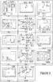
- the high-frequency module 10 includes a laminated body 900.
- the SAW duplexers DUPL and DUPH and the switch element SWIC are mounted in the upper surface of the laminated body 900.
- mount inductor elements are mounted that realize the inductors L1 and L3.
- the substantially linear electrode pattern of the inductor L2 is formed so as to rotate from an end portion on a side connecting to the common terminal PIC0, in a clockwise fashion. End portions on the side connecting to the common terminal PIC0 and on an opposite side are connected to an electrode pattern configuring the inductor L2 in the eighth layer PL8, through via electrodes penetrating electrodes in the seventh layer PL7.
- the inductor L2 has a shape winding in a clockwise fashion so as to be headed from the seventh layer PL7 to the tenth layer PL10.
- the inductor L2 when the inductor L2 is formed with the common terminal PICO of the switch element SWIC as a starting point so as to wind in a substantially spiral shape clockwise from the upper surface side of the laminated body 900 to the bottom surface side thereof, the inductors GLt1, GLt2, DLt1, and DLt2 are formed with the first individual external terminal PMtL and the second individual external terminal PMtH as starting points so as to wind in a substantially spiral shape clockwise from the upper surface side of the laminated body 900 to the bottom surface side thereof, the first individual external terminal PMtL and the second individual external terminal PMtH serving as the input ends of the transmission signals.
Landscapes
- Engineering & Computer Science (AREA)
- Computer Networks & Wireless Communication (AREA)
- Signal Processing (AREA)
- Transceivers (AREA)
- Filters And Equalizers (AREA)
- Coils Or Transformers For Communication (AREA)
Claims (7)
- Ein Hochfrequenzmodul, das folgende Merkmale aufweist:einen laminierten Körper (900), der dazu konfiguriert ist, einen Antennenverbindungs-Außenanschluss (PMan), der eine Verbindung mit einer Antenne herstellt, und eine Mehrzahl einzelner Außenanschlüsse (PMtL, PMtH) zu umfassen, mit denen jeweils eine Sendeschaltung, die zum Senden einer Mehrzahl von Kommunikationssignalen verwendet wird, und eine Empfangsschaltung, die zum Empfangen der mehreren Kommunikationssignale verwendet wird, verbunden sind; undein Schaltelement (SWIC), das dazu konfiguriert ist, in dem laminierten Körper (900) befestigt zu sein und einen gemeinsamen Anschluss (PIC0), der eine Verbindung mit dem Antennenverbindungs-Außenanschluss (PMan) herstellt, und eine Mehrzahl einzelner Anschlüsse (PIC11, PIC12) zu umfassen, die eine Verbindung mit den mehreren einzelnen Außenanschlüssen (PMtL, PMtH) herstellen, wobeidas Hochfrequenzmodul auf einer Seite der einzelnen Anschlüsse eine Mehrzahl von Induktoren (GLt1, GLt2, DLt1, DLt2) umfasst, die innerhalb des laminierten Körpers (900) gebildet sind und zwischen die mehreren einzelnen Anschlüssen (PIC11, PIC12) und die mehreren einzelnen Außenanschlüsse (PMtL, PMtH) einzeln in Reihe geschaltet sind,dadurch gekennzeichnet, dassdie mehreren Induktoren (GLt1, GLt2, DLt1, DLt2) auf der Seite der einzelnen Anschlüsse in einem Zustand, bei dem der laminierte Körper (900) entlang einer Laminierungsrichtung betrachtet wird, einander nicht überlappen und innerhalb des laminierten Körpers (900) so gebildet sind, dass Richtungen erzeugter Magnetfelder miteinander übereinstimmen.
- Das Hochfrequenzmodul gemäß Anspruch 1, das ferner folgende Merkmale aufweist:einen Induktor (L2) auf einer Seite der Antenne, der dazu konfiguriert ist, zwischen dem Antennenverbindungs-Außenanschluss (PMan) und dem gemeinsamen Anschluss (PIC0) in Reihe geschaltet zu sein, wobeider Induktor (L2) auf der Seite der Antenne und die mehreren Induktoren (GLt1, GLt2, DLt1, DLt2) auf der Seite der einzelnen Anschlüsse in einem Zustand, bei dem der laminierte Körper (900) entlang der Laminierungsrichtung betrachtet wird, einander nicht überlappen und innerhalb des laminierten Körpers (900) so gebildet sind, dass Richtungen erzeugter Magnetfelder miteinander übereinstimmen.
- Das Hochdruckfrequenzmodul gemäß einem der Ansprüche 1 und 2, bei dem
Innenschicht-Elektrodenstrukturen der mehreren Induktoren (GLt1, GLt2, DLt1, DLt2) auf der Seite der einzelnen Anschlüsse in einer Mehrzahl gleicher Schichten (PL7, PL8, PL9, PL10) des laminierten Körpers (900) gebildet sind. - Das Hochfrequenzmodul gemäß Anspruch 3, bei dem
eine Innenschicht-Elektrodenstruktur des Induktors (L2) auf der Seite der Antenne und die Innenschicht-Elektrodenstrukturen der mehreren Induktoren (GLt1, GLt2, DLt1, DLt2) auf der Seite der einzelnen Anschlüsse in den mehreren gleichen Schichten (PL7, PL8, PL9, PL10) des laminierten Körpers (900) gebildet sind, und
Abstände zwischen der Innenschicht-Elektrodenstruktur des Induktors (L2) auf der Seite der Antenne und den Innenschicht-Elektrodenstrukturen der mehreren Induktoren (GLt1, GLt2, DLt1, DLt2) auf der Seite der einzelnen Anschlüsse in einem Zustand, bei dem dieselben in der Laminierungsrichtung betrachtet werden, länger sind als Abstände zwischen den Innenschicht-Elektrodenstrukturen der mehreren Induktoren (GLt1, GLt2, DLt1, DLt2) auf der Seite der einzelnen Anschlüsse. - Das Hochfrequenzmodul gemäß einem der Ansprüche 3 und 4, das ferner folgende Merkmale aufweist:Innenschicht-Masseelektroden (GND), die dazu konfiguriert sind, in einer oberen Schicht (PL5) und einer unteren Schicht (PL13) einer Schicht gebildet zu sein, in der die Innenschicht-Elektrodenstrukturen der Induktoren (GLt1, GLt2, DLt1, DLt2, L2) in dem laminierten Körper (900) gebildet sind, um einen bildenden Bereich der Innenschicht-Elektrodenstrukturen der Induktoren (GLt1, GLt2, DLt1, DLt2, L2) zu beinhalten, wenn dieselben aus der Laminierungsrichtung betrachtet werden, wobeiein Abstand zwischen der Innenschicht-Elektrodenstruktur des am nächsten zu der Innenschicht-Masseelektrode (GND) gelegenen Induktors und der InnenschichtMasseelektrode (GND) kürzer ist als Abstände zwischen den InnenschichtElektrodenstrukturen, die einzeln die mehreren Induktoren (GLt1, GLt2, DLt1, DLt2, L2) bilden.
- Das Hochfrequenzmodul gemäß einem der Ansprüche 1 bis 5, bei dem
die mehreren Induktoren (GLt1, GLt2, DLt1, DLt2) auf der Seite der einzelnen Anschlüsse Induktoren einer Filterschaltung sind, die mit der Sendeschaltung verbunden ist. - Das Hochfrequenzmodul gemäß Anspruch 6, bei dem
die Filterschaltung ein Tiefpassfilter ist, das eine zweite harmonische Welle und eine dritte harmonische Welle eines übertragenen Kommunikationssignals dämpft, und
die mehreren Induktoren (GLt1, GLt2, DLt1, DLt2) auf der Seite der einzelnen Anschlüsse einen Reiheninduktor, der zum Dämpfen der zweiten harmonischen Welle verwendet wird, und einen Reiheninduktor umfassen, der zum Dämpfen der dritten harmonischen Welle verwendet wird.
Applications Claiming Priority (1)
| Application Number | Priority Date | Filing Date | Title |
|---|---|---|---|
| JP2011028060A JP5304811B2 (ja) | 2011-02-14 | 2011-02-14 | 高周波モジュール |
Publications (2)
| Publication Number | Publication Date |
|---|---|
| EP2487802A1 EP2487802A1 (de) | 2012-08-15 |
| EP2487802B1 true EP2487802B1 (de) | 2017-02-01 |
Family
ID=45566935
Family Applications (1)
| Application Number | Title | Priority Date | Filing Date |
|---|---|---|---|
| EP12155137.8A Not-in-force EP2487802B1 (de) | 2011-02-14 | 2012-02-13 | Hochfrequenzmodul |
Country Status (5)
| Country | Link |
|---|---|
| US (1) | US8831535B2 (de) |
| EP (1) | EP2487802B1 (de) |
| JP (1) | JP5304811B2 (de) |
| KR (1) | KR101350766B1 (de) |
| CN (1) | CN102684729B (de) |
Families Citing this family (6)
| Publication number | Priority date | Publication date | Assignee | Title |
|---|---|---|---|---|
| CN106788307A (zh) * | 2016-12-02 | 2017-05-31 | 北京北广科技股份有限公司 | 一种谐波抑制电路 |
| WO2018110393A1 (ja) * | 2016-12-14 | 2018-06-21 | 株式会社村田製作所 | スイッチic、フロントエンドモジュール及び通信装置 |
| WO2019235276A1 (ja) * | 2018-06-06 | 2019-12-12 | 株式会社村田製作所 | マルチプレクサ |
| WO2021002238A1 (ja) * | 2019-07-03 | 2021-01-07 | 株式会社村田製作所 | 高周波モジュール及び通信装置 |
| WO2021039014A1 (ja) | 2019-08-28 | 2021-03-04 | 株式会社村田製作所 | 高周波モジュール及び通信装置 |
| WO2021100259A1 (ja) * | 2019-11-20 | 2021-05-27 | 株式会社村田製作所 | 高周波回路、高周波フロントエンド回路及び通信装置 |
Family Cites Families (17)
| Publication number | Priority date | Publication date | Assignee | Title |
|---|---|---|---|---|
| JP2001267128A (ja) | 2000-03-17 | 2001-09-28 | Matsushita Electric Ind Co Ltd | 高周波積層電子部品 |
| JP3896284B2 (ja) * | 2001-02-27 | 2007-03-22 | 日本特殊陶業株式会社 | 高周波回路基板及びそれを用いた高周波用アンテナスイッチモジュール |
| DE60334888D1 (de) * | 2002-01-31 | 2010-12-23 | Hitachi Metals Ltd | Schaltnetzwerk und zusammengesetzter hochfrequenzteil |
| JP2004007408A (ja) * | 2002-01-31 | 2004-01-08 | Hitachi Metals Ltd | スイッチ回路及び複合高周波部品 |
| WO2004055841A1 (ja) * | 2002-12-13 | 2004-07-01 | Matsushita Electric Industrial Co., Ltd. | 多連チョークコイルおよびそれを用いた電子機器 |
| JP2004281847A (ja) * | 2003-03-18 | 2004-10-07 | Tdk Corp | 積層複合電子部品 |
| JP2005020140A (ja) | 2003-06-24 | 2005-01-20 | Ngk Spark Plug Co Ltd | アンテナスイッチモジュール及びそれを用いた無線電話通信装置 |
| US7596357B2 (en) | 2004-02-27 | 2009-09-29 | Kyocera Corporation | High-frequency switching circuit, high-frequency module, and wireless communications device |
| ATE417410T1 (de) | 2004-11-25 | 2008-12-15 | Murata Manufacturing Co | Hochfrequenzschaltmodul |
| WO2007049788A1 (ja) * | 2005-10-28 | 2007-05-03 | Hitachi Metals, Ltd. | Dc-dcコンバータ |
| JP4618461B2 (ja) | 2006-05-08 | 2011-01-26 | 日立金属株式会社 | 高周波回路、高周波部品及び通信装置 |
| JP2008010995A (ja) | 2006-06-28 | 2008-01-17 | Ngk Spark Plug Co Ltd | アンテナスイッチモジュール |
| CN101573881B (zh) * | 2006-12-21 | 2013-04-17 | 株式会社村田制作所 | 高频开关电路 |
| WO2009157283A1 (ja) | 2008-06-25 | 2009-12-30 | 株式会社村田製作所 | 高周波モジュール |
| KR101575387B1 (ko) * | 2009-03-18 | 2015-12-07 | 에이저 시스템즈 엘엘시 | 집적 회로 인덕터 구조체, 전자 시스템 및 집적 회로 인덕터 사이의 자기 커플링 감소 방법 |
| JP4873046B2 (ja) | 2009-05-26 | 2012-02-08 | 株式会社村田製作所 | 高周波モジュール |
| JP5136532B2 (ja) | 2009-09-29 | 2013-02-06 | 株式会社村田製作所 | 高周波スイッチモジュール |
-
2011
- 2011-02-14 JP JP2011028060A patent/JP5304811B2/ja not_active Expired - Fee Related
-
2012
- 2012-02-09 KR KR1020120013172A patent/KR101350766B1/ko not_active Expired - Fee Related
- 2012-02-13 CN CN201210052498.7A patent/CN102684729B/zh not_active Expired - Fee Related
- 2012-02-13 US US13/371,647 patent/US8831535B2/en active Active
- 2012-02-13 EP EP12155137.8A patent/EP2487802B1/de not_active Not-in-force
Non-Patent Citations (1)
| Title |
|---|
| None * |
Also Published As
| Publication number | Publication date |
|---|---|
| US8831535B2 (en) | 2014-09-09 |
| CN102684729A (zh) | 2012-09-19 |
| KR20120093080A (ko) | 2012-08-22 |
| JP5304811B2 (ja) | 2013-10-02 |
| US20120208475A1 (en) | 2012-08-16 |
| KR101350766B1 (ko) | 2014-01-13 |
| JP2012169798A (ja) | 2012-09-06 |
| CN102684729B (zh) | 2015-09-09 |
| EP2487802A1 (de) | 2012-08-15 |
Similar Documents
| Publication | Publication Date | Title |
|---|---|---|
| EP2662985B1 (de) | Hochfrequenzmodul | |
| JP5316544B2 (ja) | 高周波回路、高周波部品、及びマルチバンド通信装置 | |
| KR101798092B1 (ko) | 고주파 모듈 및 통신 장치 | |
| US9917615B2 (en) | Radio-frequency module | |
| CN100536328C (zh) | 平衡-不平衡型多频带滤波模块 | |
| JP5625453B2 (ja) | 高周波スイッチモジュール | |
| US8805299B2 (en) | High-frequency module | |
| JP5708804B2 (ja) | 高周波モジュール | |
| US20120300679A1 (en) | Communication module | |
| JP5590135B2 (ja) | 高周波モジュール | |
| CN103404040B (zh) | 高频开关模块 | |
| JP5590134B2 (ja) | 高周波モジュール | |
| EP2487802B1 (de) | Hochfrequenzmodul | |
| JP2013258516A (ja) | フィルタモジュール及び分波器モジュール | |
| JP4702620B2 (ja) | 高周波スイッチモジュール | |
| WO2009157283A1 (ja) | 高周波モジュール | |
| JP5790852B2 (ja) | 高周波スイッチモジュール |
Legal Events
| Date | Code | Title | Description |
|---|---|---|---|
| PUAI | Public reference made under article 153(3) epc to a published international application that has entered the european phase |
Free format text: ORIGINAL CODE: 0009012 |
|
| AK | Designated contracting states |
Kind code of ref document: A1 Designated state(s): AL AT BE BG CH CY CZ DE DK EE ES FI FR GB GR HR HU IE IS IT LI LT LU LV MC MK MT NL NO PL PT RO RS SE SI SK SM TR |
|
| AX | Request for extension of the european patent |
Extension state: BA ME |
|
| 17P | Request for examination filed |
Effective date: 20130215 |
|
| GRAP | Despatch of communication of intention to grant a patent |
Free format text: ORIGINAL CODE: EPIDOSNIGR1 |
|
| INTG | Intention to grant announced |
Effective date: 20160811 |
|
| GRAS | Grant fee paid |
Free format text: ORIGINAL CODE: EPIDOSNIGR3 |
|
| GRAA | (expected) grant |
Free format text: ORIGINAL CODE: 0009210 |
|
| AK | Designated contracting states |
Kind code of ref document: B1 Designated state(s): AL AT BE BG CH CY CZ DE DK EE ES FI FR GB GR HR HU IE IS IT LI LT LU LV MC MK MT NL NO PL PT RO RS SE SI SK SM TR |
|
| REG | Reference to a national code |
Ref country code: GB Ref legal event code: FG4D |
|
| REG | Reference to a national code |
Ref country code: CH Ref legal event code: EP Ref country code: AT Ref legal event code: REF Ref document number: 866326 Country of ref document: AT Kind code of ref document: T Effective date: 20170215 |
|
| REG | Reference to a national code |
Ref country code: IE Ref legal event code: FG4D |
|
| REG | Reference to a national code |
Ref country code: DE Ref legal event code: R096 Ref document number: 602012028142 Country of ref document: DE |
|
| REG | Reference to a national code |
Ref country code: NL Ref legal event code: MP Effective date: 20170201 |
|
| REG | Reference to a national code |
Ref country code: LT Ref legal event code: MG4D |
|
| REG | Reference to a national code |
Ref country code: AT Ref legal event code: MK05 Ref document number: 866326 Country of ref document: AT Kind code of ref document: T Effective date: 20170201 |
|
| PG25 | Lapsed in a contracting state [announced via postgrant information from national office to epo] |
Ref country code: GR Free format text: LAPSE BECAUSE OF FAILURE TO SUBMIT A TRANSLATION OF THE DESCRIPTION OR TO PAY THE FEE WITHIN THE PRESCRIBED TIME-LIMIT Effective date: 20170502 Ref country code: IS Free format text: LAPSE BECAUSE OF FAILURE TO SUBMIT A TRANSLATION OF THE DESCRIPTION OR TO PAY THE FEE WITHIN THE PRESCRIBED TIME-LIMIT Effective date: 20170601 Ref country code: NO Free format text: LAPSE BECAUSE OF FAILURE TO SUBMIT A TRANSLATION OF THE DESCRIPTION OR TO PAY THE FEE WITHIN THE PRESCRIBED TIME-LIMIT Effective date: 20170501 Ref country code: LT Free format text: LAPSE BECAUSE OF FAILURE TO SUBMIT A TRANSLATION OF THE DESCRIPTION OR TO PAY THE FEE WITHIN THE PRESCRIBED TIME-LIMIT Effective date: 20170201 Ref country code: HR Free format text: LAPSE BECAUSE OF FAILURE TO SUBMIT A TRANSLATION OF THE DESCRIPTION OR TO PAY THE FEE WITHIN THE PRESCRIBED TIME-LIMIT Effective date: 20170201 Ref country code: FI Free format text: LAPSE BECAUSE OF FAILURE TO SUBMIT A TRANSLATION OF THE DESCRIPTION OR TO PAY THE FEE WITHIN THE PRESCRIBED TIME-LIMIT Effective date: 20170201 |
|
| PG25 | Lapsed in a contracting state [announced via postgrant information from national office to epo] |
Ref country code: LV Free format text: LAPSE BECAUSE OF FAILURE TO SUBMIT A TRANSLATION OF THE DESCRIPTION OR TO PAY THE FEE WITHIN THE PRESCRIBED TIME-LIMIT Effective date: 20170201 Ref country code: NL Free format text: LAPSE BECAUSE OF FAILURE TO SUBMIT A TRANSLATION OF THE DESCRIPTION OR TO PAY THE FEE WITHIN THE PRESCRIBED TIME-LIMIT Effective date: 20170201 Ref country code: PT Free format text: LAPSE BECAUSE OF FAILURE TO SUBMIT A TRANSLATION OF THE DESCRIPTION OR TO PAY THE FEE WITHIN THE PRESCRIBED TIME-LIMIT Effective date: 20170601 Ref country code: AT Free format text: LAPSE BECAUSE OF FAILURE TO SUBMIT A TRANSLATION OF THE DESCRIPTION OR TO PAY THE FEE WITHIN THE PRESCRIBED TIME-LIMIT Effective date: 20170201 Ref country code: BG Free format text: LAPSE BECAUSE OF FAILURE TO SUBMIT A TRANSLATION OF THE DESCRIPTION OR TO PAY THE FEE WITHIN THE PRESCRIBED TIME-LIMIT Effective date: 20170501 Ref country code: RS Free format text: LAPSE BECAUSE OF FAILURE TO SUBMIT A TRANSLATION OF THE DESCRIPTION OR TO PAY THE FEE WITHIN THE PRESCRIBED TIME-LIMIT Effective date: 20170201 Ref country code: SE Free format text: LAPSE BECAUSE OF FAILURE TO SUBMIT A TRANSLATION OF THE DESCRIPTION OR TO PAY THE FEE WITHIN THE PRESCRIBED TIME-LIMIT Effective date: 20170201 Ref country code: PL Free format text: LAPSE BECAUSE OF FAILURE TO SUBMIT A TRANSLATION OF THE DESCRIPTION OR TO PAY THE FEE WITHIN THE PRESCRIBED TIME-LIMIT Effective date: 20170201 Ref country code: ES Free format text: LAPSE BECAUSE OF FAILURE TO SUBMIT A TRANSLATION OF THE DESCRIPTION OR TO PAY THE FEE WITHIN THE PRESCRIBED TIME-LIMIT Effective date: 20170201 |
|
| REG | Reference to a national code |
Ref country code: CH Ref legal event code: PL |
|
| PG25 | Lapsed in a contracting state [announced via postgrant information from national office to epo] |
Ref country code: CZ Free format text: LAPSE BECAUSE OF FAILURE TO SUBMIT A TRANSLATION OF THE DESCRIPTION OR TO PAY THE FEE WITHIN THE PRESCRIBED TIME-LIMIT Effective date: 20170201 Ref country code: LI Free format text: LAPSE BECAUSE OF NON-PAYMENT OF DUE FEES Effective date: 20170228 Ref country code: RO Free format text: LAPSE BECAUSE OF FAILURE TO SUBMIT A TRANSLATION OF THE DESCRIPTION OR TO PAY THE FEE WITHIN THE PRESCRIBED TIME-LIMIT Effective date: 20170201 Ref country code: EE Free format text: LAPSE BECAUSE OF FAILURE TO SUBMIT A TRANSLATION OF THE DESCRIPTION OR TO PAY THE FEE WITHIN THE PRESCRIBED TIME-LIMIT Effective date: 20170201 Ref country code: SK Free format text: LAPSE BECAUSE OF FAILURE TO SUBMIT A TRANSLATION OF THE DESCRIPTION OR TO PAY THE FEE WITHIN THE PRESCRIBED TIME-LIMIT Effective date: 20170201 Ref country code: IT Free format text: LAPSE BECAUSE OF FAILURE TO SUBMIT A TRANSLATION OF THE DESCRIPTION OR TO PAY THE FEE WITHIN THE PRESCRIBED TIME-LIMIT Effective date: 20170201 Ref country code: CH Free format text: LAPSE BECAUSE OF NON-PAYMENT OF DUE FEES Effective date: 20170228 |
|
| REG | Reference to a national code |
Ref country code: DE Ref legal event code: R097 Ref document number: 602012028142 Country of ref document: DE |
|
| REG | Reference to a national code |
Ref country code: IE Ref legal event code: MM4A |
|
| PG25 | Lapsed in a contracting state [announced via postgrant information from national office to epo] |
Ref country code: MC Free format text: LAPSE BECAUSE OF FAILURE TO SUBMIT A TRANSLATION OF THE DESCRIPTION OR TO PAY THE FEE WITHIN THE PRESCRIBED TIME-LIMIT Effective date: 20170201 Ref country code: SM Free format text: LAPSE BECAUSE OF FAILURE TO SUBMIT A TRANSLATION OF THE DESCRIPTION OR TO PAY THE FEE WITHIN THE PRESCRIBED TIME-LIMIT Effective date: 20170201 Ref country code: DK Free format text: LAPSE BECAUSE OF FAILURE TO SUBMIT A TRANSLATION OF THE DESCRIPTION OR TO PAY THE FEE WITHIN THE PRESCRIBED TIME-LIMIT Effective date: 20170201 |
|
| PLBE | No opposition filed within time limit |
Free format text: ORIGINAL CODE: 0009261 |
|
| STAA | Information on the status of an ep patent application or granted ep patent |
Free format text: STATUS: NO OPPOSITION FILED WITHIN TIME LIMIT |
|
| PG25 | Lapsed in a contracting state [announced via postgrant information from national office to epo] |
Ref country code: LU Free format text: LAPSE BECAUSE OF NON-PAYMENT OF DUE FEES Effective date: 20170213 |
|
| 26N | No opposition filed |
Effective date: 20171103 |
|
| REG | Reference to a national code |
Ref country code: FR Ref legal event code: ST Effective date: 20171220 |
|
| GBPC | Gb: european patent ceased through non-payment of renewal fee |
Effective date: 20170501 |
|
| PG25 | Lapsed in a contracting state [announced via postgrant information from national office to epo] |
Ref country code: FR Free format text: LAPSE BECAUSE OF NON-PAYMENT OF DUE FEES Effective date: 20170403 |
|
| REG | Reference to a national code |
Ref country code: BE Ref legal event code: MM Effective date: 20170228 |
|
| PG25 | Lapsed in a contracting state [announced via postgrant information from national office to epo] |
Ref country code: SI Free format text: LAPSE BECAUSE OF FAILURE TO SUBMIT A TRANSLATION OF THE DESCRIPTION OR TO PAY THE FEE WITHIN THE PRESCRIBED TIME-LIMIT Effective date: 20170201 Ref country code: IE Free format text: LAPSE BECAUSE OF NON-PAYMENT OF DUE FEES Effective date: 20170213 |
|
| PG25 | Lapsed in a contracting state [announced via postgrant information from national office to epo] |
Ref country code: GB Free format text: LAPSE BECAUSE OF NON-PAYMENT OF DUE FEES Effective date: 20170501 |
|
| PG25 | Lapsed in a contracting state [announced via postgrant information from national office to epo] |
Ref country code: BE Free format text: LAPSE BECAUSE OF NON-PAYMENT OF DUE FEES Effective date: 20170228 |
|
| PG25 | Lapsed in a contracting state [announced via postgrant information from national office to epo] |
Ref country code: MT Free format text: LAPSE BECAUSE OF NON-PAYMENT OF DUE FEES Effective date: 20170213 |
|
| PG25 | Lapsed in a contracting state [announced via postgrant information from national office to epo] |
Ref country code: HU Free format text: LAPSE BECAUSE OF FAILURE TO SUBMIT A TRANSLATION OF THE DESCRIPTION OR TO PAY THE FEE WITHIN THE PRESCRIBED TIME-LIMIT; INVALID AB INITIO Effective date: 20120213 |
|
| PG25 | Lapsed in a contracting state [announced via postgrant information from national office to epo] |
Ref country code: CY Free format text: LAPSE BECAUSE OF NON-PAYMENT OF DUE FEES Effective date: 20170201 |
|
| PG25 | Lapsed in a contracting state [announced via postgrant information from national office to epo] |
Ref country code: MK Free format text: LAPSE BECAUSE OF FAILURE TO SUBMIT A TRANSLATION OF THE DESCRIPTION OR TO PAY THE FEE WITHIN THE PRESCRIBED TIME-LIMIT Effective date: 20170201 |
|
| PG25 | Lapsed in a contracting state [announced via postgrant information from national office to epo] |
Ref country code: TR Free format text: LAPSE BECAUSE OF FAILURE TO SUBMIT A TRANSLATION OF THE DESCRIPTION OR TO PAY THE FEE WITHIN THE PRESCRIBED TIME-LIMIT Effective date: 20170201 |
|
| PG25 | Lapsed in a contracting state [announced via postgrant information from national office to epo] |
Ref country code: AL Free format text: LAPSE BECAUSE OF FAILURE TO SUBMIT A TRANSLATION OF THE DESCRIPTION OR TO PAY THE FEE WITHIN THE PRESCRIBED TIME-LIMIT Effective date: 20170201 |
|
| PGFP | Annual fee paid to national office [announced via postgrant information from national office to epo] |
Ref country code: DE Payment date: 20220217 Year of fee payment: 11 |
|
| REG | Reference to a national code |
Ref country code: DE Ref legal event code: R119 Ref document number: 602012028142 Country of ref document: DE |
|
| PG25 | Lapsed in a contracting state [announced via postgrant information from national office to epo] |
Ref country code: DE Free format text: LAPSE BECAUSE OF NON-PAYMENT OF DUE FEES Effective date: 20230901 |