EP2490352A1 - Dispositif et procédé de commande d'amplitude de pilotage d'un émetteur à modulation différentielle par déplacement de phase en quadrature - Google Patents
Dispositif et procédé de commande d'amplitude de pilotage d'un émetteur à modulation différentielle par déplacement de phase en quadrature Download PDFInfo
- Publication number
- EP2490352A1 EP2490352A1 EP10788981A EP10788981A EP2490352A1 EP 2490352 A1 EP2490352 A1 EP 2490352A1 EP 10788981 A EP10788981 A EP 10788981A EP 10788981 A EP10788981 A EP 10788981A EP 2490352 A1 EP2490352 A1 EP 2490352A1
- Authority
- EP
- European Patent Office
- Prior art keywords
- driver
- change
- drain voltage
- controlling
- mosfet
- Prior art date
- Legal status (The legal status is an assumption and is not a legal conclusion. Google has not performed a legal analysis and makes no representation as to the accuracy of the status listed.)
- Granted
Links
Images


Classifications
-
- H—ELECTRICITY
- H04—ELECTRIC COMMUNICATION TECHNIQUE
- H04B—TRANSMISSION
- H04B10/00—Transmission systems employing electromagnetic waves other than radio-waves, e.g. infrared, visible or ultraviolet light, or employing corpuscular radiation, e.g. quantum communication
- H04B10/50—Transmitters
- H04B10/516—Details of coding or modulation
- H04B10/548—Phase or frequency modulation
- H04B10/556—Digital modulation, e.g. differential phase shift keying [DPSK] or frequency shift keying [FSK]
- H04B10/5561—Digital phase modulation
-
- H—ELECTRICITY
- H04—ELECTRIC COMMUNICATION TECHNIQUE
- H04B—TRANSMISSION
- H04B10/00—Transmission systems employing electromagnetic waves other than radio-waves, e.g. infrared, visible or ultraviolet light, or employing corpuscular radiation, e.g. quantum communication
- H04B10/50—Transmitters
- H04B10/501—Structural aspects
- H04B10/503—Laser transmitters
- H04B10/505—Laser transmitters using external modulation
- H04B10/5053—Laser transmitters using external modulation using a parallel, i.e. shunt, combination of modulators
-
- H—ELECTRICITY
- H04—ELECTRIC COMMUNICATION TECHNIQUE
- H04B—TRANSMISSION
- H04B10/00—Transmission systems employing electromagnetic waves other than radio-waves, e.g. infrared, visible or ultraviolet light, or employing corpuscular radiation, e.g. quantum communication
- H04B10/50—Transmitters
- H04B10/501—Structural aspects
- H04B10/503—Laser transmitters
- H04B10/505—Laser transmitters using external modulation
- H04B10/5057—Laser transmitters using external modulation using a feedback signal generated by analysing the optical output
-
- H—ELECTRICITY
- H04—ELECTRIC COMMUNICATION TECHNIQUE
- H04B—TRANSMISSION
- H04B10/00—Transmission systems employing electromagnetic waves other than radio-waves, e.g. infrared, visible or ultraviolet light, or employing corpuscular radiation, e.g. quantum communication
- H04B10/50—Transmitters
- H04B10/501—Structural aspects
- H04B10/503—Laser transmitters
- H04B10/505—Laser transmitters using external modulation
- H04B10/5057—Laser transmitters using external modulation using a feedback signal generated by analysing the optical output
- H04B10/50572—Laser transmitters using external modulation using a feedback signal generated by analysing the optical output to control the modulating signal amplitude including amplitude distortion
-
- H—ELECTRICITY
- H04—ELECTRIC COMMUNICATION TECHNIQUE
- H04B—TRANSMISSION
- H04B10/00—Transmission systems employing electromagnetic waves other than radio-waves, e.g. infrared, visible or ultraviolet light, or employing corpuscular radiation, e.g. quantum communication
- H04B10/50—Transmitters
- H04B10/501—Structural aspects
- H04B10/503—Laser transmitters
- H04B10/505—Laser transmitters using external modulation
- H04B10/5057—Laser transmitters using external modulation using a feedback signal generated by analysing the optical output
- H04B10/50575—Laser transmitters using external modulation using a feedback signal generated by analysing the optical output to control the modulator DC bias
Definitions
- the present invention relates to the communications equipment, and more particularly, to an apparatus and a method for controlling driving amplitude of a differential quadrature phase shift keying transmitter.
- DQPSK Downlink Phase Shift Keying
- MZM Machine-Zender Modulator
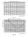
- FIG. 1 is a schematic diagram of influence of modulating driving amplitude
- FIG. 1A is a schematic diagram of an OSNR (Optical Signal Noise Ratio) tolerance curve.
- OSNR Optical Signal Noise Ratio
- FIG. 1B is a schematic diagram of a dispersion tolerance curve in simulation, and in FIG.
- the OSNR tolerance and the 2dB OSNR cost dispersion tolerance remain stable at first, and then increase rapidly, but the increasing rate is slower than that at the decreasing of the driving amplitude; and when the driving amplitude increases to 1.5Vpi, compared with the Vpi, it brings that the OSNR cost is almost 2dB, which is much larger than the case of NRZ-DPSK.
- the change of the driving amplitude has relatively large influence on the NRZ-DQPSK performance, and when the driving amplitude is 1.1Vpi, although the dispersion tolerance is minimum, its OSNR performance is the best.
- the driving amplitude is 1.1Vpi, although the dispersion tolerance is minimum, its OSNR performance is the best.
- the NRZ-DQPSK system with rate of 40Gb/s a superior OSNR performance is more concerned, thus the best driving amplitude is taken as 1.1Vpi. Therefore, the stability of the driving amplitude has a large influence on the OSNR performance of the NRZ-DQPSK transmitter, and the driving amplitude needs to be controlled strictly.
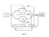
- FIG. 2 is a block diagram of a structure of a feedback control apparatus of a DQPSK transmitter.
- the CW denotes the continuous spectrum light source of the unmodulated signal
- the driver I and the driver Q denote drivers of two upper and lower Mach-Zender modulators of the DQPSK modulator
- the Bias 1, Bias 2 and Bias 3 are the bias point 1, the bias point 2 and the bias point 3.
- the light emitted from the CW is modulated by the DQPSK modulator to generate a modulated optical signal to output, wherein, a part of the modulated optical signal is used to control the states of the modulator, the driver I and the driver Q.
- the disadvantage of the related art is that: since the DQPSK transmitter needs to control the three bias points of the modulator, the control circuit is relatively complicated already, then, if the driving amplitude is controlled by using the conventional method in which the pilot signal is added and by the time division multiplexing mode, the control circuit is very large, and adding the pilot signal might introduce a certain amount of OSNR cost.
- the technical problem to be solved in the present invention is to provide an apparatus and a method for controlling driving amplitude of a differential quadrature phase shift keying transmitter, so as to simplify the complexity of the control circuit of the DQPSK transmitter.
- the present invention provides an apparatus for controlling driving amplitude of a DQPSK transmitter, and the apparatus comprises: a first bias point, a second bias point, a third bias point, a driver I, a driver Q, and a DQPSK modulator for modulating an optical signal emitted by the CW, the apparatus also comprises:
- the driver I feedback control unit comprises:
- the driver Q feedback control unit comprises:
- the temperature compensation curve is obtained according to the driving amplitude of an output signal of the driver and the drain voltage of the MOSFET of the driver.
- the driver I feedback control unit comprises:
- driver Q feedback control unit comprises:
- the present invention provides a method for controlling driving amplitude of a DQPSK transmitter, and the method comprises:
- controlling the driving amplitude of the driver I according to the temperature change of the driver I comprises:
- the temperature compensation curve is obtained according to the driving amplitude of an output signal of the driver and the drain voltage of the MOSFET of the driver.
- controlling the driving amplitude of the driver I according to the temperature change of the driver I comprises:
- embodiments of the present invention provide a new technique for monitoring and controlling the driving amplitude, to simplify multiple intercoupling control circuits of the DQPSK transmitter, and to get rid of the mode in which the original driving amplitude control needs to use the modulator to feed back, but some signals of the driver itself are only needed to act as the feedback signals to control the driving amplitude.
- the specific embodiments of the present invention will be illustrated in combination with the accompanying drawings.
- FIG. 3 is a structural diagram of an apparatus for controlling driving amplitude of a DQPSK transmitter.
- the apparatus comprises: the first bias point Bias1, the second bias point Bias2, the third bias point Bias3, the driver I, the driver Q, and the DQPSK modulator which modulates the optical signal emitted from the CW, and the apparatus also comprises:
- the modulator feedback control unit does not detach a part of the modulated optical signal to control the states of the driver I and the driver Q
- the driver amplitude control circuit is separated from the feedback control of the DQPSK modulator, and other feedback signals are used to control the driving amplitude, that is: the driving amplitude of the driver is controlled according to the temperature change of the driver.
- FIG. 4 is a schematic diagram of a driver feedback control in a direct compensation mode.
- the driver has three levels, and each level is considered as a MOSFET (Metal Oxide Semiconductor Field Effect Transistor); VD3 is a drain voltage of the third-level MOSFET, VD2 is a drain voltage of the second-level MOSFET, and VD1 is a drain voltage of the first-level MOSFET.
- MOSFET Metal Oxide Semiconductor Field Effect Transistor
- the DC-DC is a switching power supply converter
- Vin is an input voltage converted by the DC-DC power supply.
- the TEMP SENSOR is a temperature sensor.
- the VG is a gate voltage of the MOSFET.
- the DAC is a Digital to Analog Converter.
- the driving amplitude of this driver is related to the VD3, thus the temperature sensor can be used to detect the temperature of the driver, and then a temperature compensation algorithm is used to change the feedback network of DC-DC, thus changing the value of the VD3, so as to ensure the driving amplitude of the driver unchanged.
- the process is that: the temperature sensor firstly detects the temperature of the driver, and calculates an offset of the VD3 by using the temperature compensation algorithm, then the DAC feeds back the offset to the DC-DC, and then the DC-DC controls the output voltage so as to change the value of the VD3.
- the driver I and the driver Q can individually use the temperature control circuit to control the driving amplitude.
- the modulator feedback control unit can use any control mode which will not affect the driver control circuit.
- FIG. 5 is a schematic diagram of a temperature compensation curve in a direct compensation mode.
- EYE-AMP is the driving amplitude of the output signal of the driver
- C is the Celsius temperature
- VD is the drain voltage of the MOSFET of the driver.
- the temperature compensation curve can be used to change the feedback network of the DC-DC, that is, the temperature compensation curve can be obtained according to the driving amplitude of the output signal of the driver and the drain voltage of the MOSFET of the driver, so as to be used for temperature compensation.
- control for the driver I and/or the driver Q can be as follows.
- the driver I feedback control unit can comprise:
- the driver Q feedback control unit can comprise:
- FIG. 6 is a schematic diagram of a driver feedback control in an indirect compensation mode.
- the driver has three levels, wherein, the VD3 is the drain voltage of the third-level MOSFET, the VD2 is the drain voltage of the second-level MOSFET, and the VD1 is the drain voltage of the first-level MOSFET.
- the DC-DC is a switching power supply converter
- Vin is the input voltage converted by the DC-DC power supply.
- the Current Monitor is a current monitor.
- the VG is the gate voltage of the MOSFET.
- the DAC is a Digital to Analog Converter.
- the driving amplitude of the driver changes due to the influence of the temperature
- the current through the VD3 might change, so that whether the driving amplitude of the driver changes can be indirectly detected by monitoring the current of the VD3. If the current change is monitored, then the current of the VD3 can be corrected by changing the voltage of the VG3, to guarantee the current of the VD3 unchanged, thus the driving amplitude of the driver is controlled.
- the driver I and the driver Q can individually use the temperature control circuit to control the driving amplitude.
- the modulator feedback control unit can use any control mode which will not affect the driver control circuit.
- control for the driver I and/or the driver Q can be as follows.
- the driver I feedback control unit can comprise:
- the driver Q feedback control unit can comprise:
- the control mode of the direct compensation mode is simple, and the feedback control can be executed as long as the whole temperature range of the compensation curve of the driver is known.
- the control mode of the indirect compensation mode is relatively complicated, and the feedback control is executed which is required to use the current monitoring mode.
- the control accuracy of the indirect compensation mode is higher than that of the direct compensation mode, and the driving amplitude can be controlled by monitoring the tiny change in current.
- different control modes can be applied according to different application scenarios.
- the direct compensation and indirect compensation are taken for example to illustrate in the implementation, but in theory, other modes might be also used, as long as the driving amplitude of the driver can be controlled according to the temperature change of the driver; and the direct compensation and the indirect compensation are only used to teach those skilled in the art how to implement the present invention, which are not intended to user the two modes only, and in the implementation process, an appropriate mode might be determined in combination with the practical requirement.
- the embodiments of the present invention also provides a method for controlling the driving amplitude of the DQPSK transmitter. Since the principle of this method to solve the problem is similar to the apparatus for controlling the driving amplitude of the DQPSK transmitter, the implementation of this method can refer to the implementation of the apparatus and the repeated places are not repeated here.
- FIG. 7 is a diagram of an implementation process of a method for controlling driving amplitude of a DQPSK transmitter, and as shown in FIG. 7 , the following steps can be comprised when controlling the driving amplitude:
- controlling the driving amplitude of the driver I according to the temperature change of the driver I can comprise:
- controlling the driving amplitude of the driver Q according to the temperature change of the driver Q can comprise:
- the temperature compensation curve can be obtained according to the driving amplitude of the output signal of the driver and the drain voltage of the MOSFET of the driver.
- controlling the driving amplitude of the driver I according to the temperature change of the driver I can comprise:
- controlling the driving amplitude of the driver Q according to the temperature change of the driver Q can comprise:
- the modulator feedback control unit is used to control the voltages of the three bias points of the DQPSK modulator
- the driver feedback control unit is used to individually control the driving amplitude of the driver.
- the present invention can simplify the complexity of the control circuit of the DQPSK transmitter.
- the present invention does not need to add the pilot signal on the driving amplitude of the driver, thus no extra OSNR cost would be created.
Landscapes
- Physics & Mathematics (AREA)
- Electromagnetism (AREA)
- Engineering & Computer Science (AREA)
- Computer Networks & Wireless Communication (AREA)
- Signal Processing (AREA)
- Optics & Photonics (AREA)
- Optical Communication System (AREA)
- Optical Modulation, Optical Deflection, Nonlinear Optics, Optical Demodulation, Optical Logic Elements (AREA)
- Control Of Temperature (AREA)
Applications Claiming Priority (2)
| Application Number | Priority Date | Filing Date | Title |
|---|---|---|---|
| CN2009101783239A CN101674138B (zh) | 2009-10-16 | 2009-10-16 | 差分四相相移键控发送机的驱动幅度控制装置及方法 |
| PCT/CN2010/074513 WO2010145585A1 (fr) | 2009-10-16 | 2010-06-25 | Dispositif et procédé de commande d'amplitude de pilotage d'un émetteur à modulation différentielle par déplacement de phase en quadrature |
Publications (3)
| Publication Number | Publication Date |
|---|---|
| EP2490352A1 true EP2490352A1 (fr) | 2012-08-22 |
| EP2490352A4 EP2490352A4 (fr) | 2016-06-29 |
| EP2490352B1 EP2490352B1 (fr) | 2018-10-17 |
Family
ID=42021158
Family Applications (1)
| Application Number | Title | Priority Date | Filing Date |
|---|---|---|---|
| EP10788981.8A Active EP2490352B1 (fr) | 2009-10-16 | 2010-06-25 | Dispositif et procédé de commande d'amplitude de pilotage d'un émetteur à modulation différentielle par déplacement de phase en quadrature |
Country Status (6)
| Country | Link |
|---|---|
| US (1) | US20120207483A1 (fr) |
| EP (1) | EP2490352B1 (fr) |
| JP (1) | JP2013507855A (fr) |
| KR (1) | KR20120083467A (fr) |
| CN (1) | CN101674138B (fr) |
| WO (1) | WO2010145585A1 (fr) |
Families Citing this family (10)
| Publication number | Priority date | Publication date | Assignee | Title |
|---|---|---|---|---|
| CN101674138B (zh) * | 2009-10-16 | 2013-07-03 | 中兴通讯股份有限公司 | 差分四相相移键控发送机的驱动幅度控制装置及方法 |
| CN102340468B (zh) * | 2010-07-14 | 2015-08-12 | 中兴通讯股份有限公司 | 驱动信号幅度的控制方法和装置、dqpsk发射机系统 |
| CN102055406B (zh) * | 2010-10-22 | 2014-08-13 | 中兴通讯股份有限公司 | 驱动器时序差的处理方法及装置 |
| US9344194B2 (en) * | 2013-02-21 | 2016-05-17 | Fujitsu Limited | System and method for monitoring and control of an optical modulator for an M-QAM transmitter |
| CN104485997B (zh) * | 2014-12-09 | 2017-04-12 | 华中科技大学 | 一种iq光调制器偏置电压的控制系统及方法 |
| JP6601212B2 (ja) * | 2015-12-24 | 2019-11-06 | 住友電気工業株式会社 | 光送信器 |
| JP2017116746A (ja) * | 2015-12-24 | 2017-06-29 | 富士通株式会社 | 光送信器及び制御方法 |
| US10861565B2 (en) | 2018-12-31 | 2020-12-08 | Micron Technology, Inc. | Functional signal line overdrive |
| JP7597226B2 (ja) * | 2020-12-25 | 2024-12-10 | 日本電気株式会社 | 光送信機および光送信方法 |
| JP2024058965A (ja) * | 2022-10-17 | 2024-04-30 | 日本電気株式会社 | 光通信システムにおける送信機、ネスト型変調器の制御方法およびプログラム |
Family Cites Families (16)
| Publication number | Priority date | Publication date | Assignee | Title |
|---|---|---|---|---|
| JP3476465B2 (ja) * | 1993-06-08 | 2003-12-10 | ナショナル・セミコンダクター・コーポレイション | Cmosbtl互換バス及び伝送線路ドライバ |
| JP3736953B2 (ja) * | 1997-10-20 | 2006-01-18 | 富士通株式会社 | 電界吸収型光変調器の駆動回路及び、これを用いた光送信器 |
| US6922045B2 (en) * | 2002-02-13 | 2005-07-26 | Primarion, Inc. | Current driver and method of precisely controlling output current |
| JP4083657B2 (ja) * | 2003-03-28 | 2008-04-30 | 住友大阪セメント株式会社 | 光変調器のバイアス制御方法及びその装置 |
| US6978056B2 (en) * | 2003-06-04 | 2005-12-20 | Covega, Inc. | Waveguide modulators having bias control with reduced temperature dependence |
| JP4527993B2 (ja) * | 2004-01-28 | 2010-08-18 | 日本放送協会 | 光変調装置及び光変調方法 |
| ATE390768T1 (de) * | 2005-11-25 | 2008-04-15 | Alcatel Lucent | Faseroptisches übertragungssystem, sender und empfänger für dqpsk modulierte signale und zugehöriges stabilisierungsverfahren |
| JP4781094B2 (ja) * | 2005-11-30 | 2011-09-28 | 富士通株式会社 | 光送信装置 |
| US20070212075A1 (en) * | 2006-03-09 | 2007-09-13 | Yy Labs, Inc. | Dual-parallel-mz modulator bias control |
| CN101043269B (zh) * | 2006-03-22 | 2011-01-05 | 富士通株式会社 | I-q正交调制发射机及其i-q路间相位偏置的监测装置和方法 |
| JP5405716B2 (ja) * | 2006-09-29 | 2014-02-05 | 富士通株式会社 | 光送信機 |
| US7733193B2 (en) * | 2007-11-01 | 2010-06-08 | Ciena Corporation | Systems and methods for DQPSK modulator control using selectively inserted dither tone |
| CN101276067A (zh) * | 2008-05-05 | 2008-10-01 | 中兴通讯股份有限公司 | 铌酸锂调制器的动态控制方法和装置 |
| CN101453271A (zh) * | 2008-09-03 | 2009-06-10 | 沈红 | 快速突发光发送方法 |
| JP5169710B2 (ja) * | 2008-10-10 | 2013-03-27 | 富士通株式会社 | 光受信装置および分散補償シーケンス制御方法 |
| CN101674138B (zh) * | 2009-10-16 | 2013-07-03 | 中兴通讯股份有限公司 | 差分四相相移键控发送机的驱动幅度控制装置及方法 |
-
2009
- 2009-10-16 CN CN2009101783239A patent/CN101674138B/zh active Active
-
2010
- 2010-06-25 KR KR1020127012604A patent/KR20120083467A/ko not_active Ceased
- 2010-06-25 US US13/501,595 patent/US20120207483A1/en not_active Abandoned
- 2010-06-25 JP JP2012533464A patent/JP2013507855A/ja active Pending
- 2010-06-25 EP EP10788981.8A patent/EP2490352B1/fr active Active
- 2010-06-25 WO PCT/CN2010/074513 patent/WO2010145585A1/fr not_active Ceased
Also Published As
| Publication number | Publication date |
|---|---|
| JP2013507855A (ja) | 2013-03-04 |
| US20120207483A1 (en) | 2012-08-16 |
| WO2010145585A1 (fr) | 2010-12-23 |
| CN101674138A (zh) | 2010-03-17 |
| KR20120083467A (ko) | 2012-07-25 |
| EP2490352B1 (fr) | 2018-10-17 |
| CN101674138B (zh) | 2013-07-03 |
| EP2490352A4 (fr) | 2016-06-29 |
Similar Documents
| Publication | Publication Date | Title |
|---|---|---|
| EP2490352B1 (fr) | Dispositif et procédé de commande d'amplitude de pilotage d'un émetteur à modulation différentielle par déplacement de phase en quadrature | |
| US7773283B2 (en) | Optical modulation device and optical modulation method | |
| US8098998B2 (en) | Optical transmitter | |
| US10225017B2 (en) | Optical transmitter and method for controlling the same | |
| US7840141B2 (en) | Differential M phase-shift modulator | |
| EP1906564A1 (fr) | Émetteur optique | |
| WO2013042175A1 (fr) | Dispositif de sortie optique et procédé de commande d'un émetteur optique | |
| US9853736B2 (en) | Optical transmitter and bias control method for optical modulator | |
| US20100080571A1 (en) | Optical signal transmitter | |
| US8693887B2 (en) | Optical transmitter and optical transmission system | |
| JP6217152B2 (ja) | 光送信器及び光送信器の制御方法 | |
| US6542280B2 (en) | Return-to-zero optical modulator with configurable pulse width | |
| JP5811531B2 (ja) | 光送信機、光通信システムおよび光送信方法 | |
| Tatsumi et al. | A compact low-power 224-Gb/s DP-16QAM modulator module with InP-based modulator and linear driver ICs | |
| CN112005159B (zh) | 光调制器 | |
| WO2006048944A1 (fr) | Émetteur optique et système de communication optique | |
| HK1171290A (en) | Apparatus and method for control the driving amplitude of differential quadrature phase shift keying transmitter | |
| HK1171290B (en) | Apparatus and method for control the driving amplitude of differential quadrature phase shift keying transmitter | |
| US20070092266A1 (en) | Method and apparatus for controlling bias point of optical transmitter | |
| US20120082467A1 (en) | Optical transmitter, optical transmission device, and method of controlling optical transmitter | |
| EP1610478B1 (fr) | Modulateur optique présentant des besoins réduits en largeur de bande et procédé associé | |
| JP4884338B2 (ja) | 光変調器ドライバ調整装置及び調整方法 | |
| EP1986353A1 (fr) | Transmetteur optique avec commande de polarisation du modulateur | |
| Itabashi et al. | A compact low-power 224-Gb/s DP-16QAM modulator module with InP-based modulator and linear driver ICs | |
| US20100303470A1 (en) | Optical transmitter |
Legal Events
| Date | Code | Title | Description |
|---|---|---|---|
| PUAI | Public reference made under article 153(3) epc to a published international application that has entered the european phase |
Free format text: ORIGINAL CODE: 0009012 |
|
| 17P | Request for examination filed |
Effective date: 20120322 |
|
| AK | Designated contracting states |
Kind code of ref document: A1 Designated state(s): AL AT BE BG CH CY CZ DE DK EE ES FI FR GB GR HR HU IE IS IT LI LT LU LV MC MK MT NL NO PL PT RO SE SI SK SM TR |
|
| DAX | Request for extension of the european patent (deleted) | ||
| REG | Reference to a national code |
Ref country code: HK Ref legal event code: DE Ref document number: 1171290 Country of ref document: HK |
|
| REG | Reference to a national code |
Ref country code: DE Ref legal event code: R079 Ref document number: 602010054443 Country of ref document: DE Free format text: PREVIOUS MAIN CLASS: H04B0010155000 Ipc: H04B0010500000 |
|
| RA4 | Supplementary search report drawn up and despatched (corrected) |
Effective date: 20160531 |
|
| RIC1 | Information provided on ipc code assigned before grant |
Ipc: H04B 10/50 20130101AFI20160524BHEP Ipc: H04B 10/556 20130101ALI20160524BHEP |
|
| GRAP | Despatch of communication of intention to grant a patent |
Free format text: ORIGINAL CODE: EPIDOSNIGR1 |
|
| STAA | Information on the status of an ep patent application or granted ep patent |
Free format text: STATUS: GRANT OF PATENT IS INTENDED |
|
| INTG | Intention to grant announced |
Effective date: 20180525 |
|
| GRAS | Grant fee paid |
Free format text: ORIGINAL CODE: EPIDOSNIGR3 |
|
| GRAA | (expected) grant |
Free format text: ORIGINAL CODE: 0009210 |
|
| STAA | Information on the status of an ep patent application or granted ep patent |
Free format text: STATUS: THE PATENT HAS BEEN GRANTED |
|
| AK | Designated contracting states |
Kind code of ref document: B1 Designated state(s): AL AT BE BG CH CY CZ DE DK EE ES FI FR GB GR HR HU IE IS IT LI LT LU LV MC MK MT NL NO PL PT RO SE SI SK SM TR |
|
| REG | Reference to a national code |
Ref country code: GB Ref legal event code: FG4D |
|
| REG | Reference to a national code |
Ref country code: CH Ref legal event code: EP |
|
| REG | Reference to a national code |
Ref country code: IE Ref legal event code: FG4D |
|
| REG | Reference to a national code |
Ref country code: DE Ref legal event code: R096 Ref document number: 602010054443 Country of ref document: DE Ref country code: AT Ref legal event code: REF Ref document number: 1055239 Country of ref document: AT Kind code of ref document: T Effective date: 20181115 |
|
| REG | Reference to a national code |
Ref country code: NL Ref legal event code: MP Effective date: 20181017 |
|
| REG | Reference to a national code |
Ref country code: LT Ref legal event code: MG4D |
|
| REG | Reference to a national code |
Ref country code: AT Ref legal event code: MK05 Ref document number: 1055239 Country of ref document: AT Kind code of ref document: T Effective date: 20181017 |
|
| PG25 | Lapsed in a contracting state [announced via postgrant information from national office to epo] |
Ref country code: NL Free format text: LAPSE BECAUSE OF FAILURE TO SUBMIT A TRANSLATION OF THE DESCRIPTION OR TO PAY THE FEE WITHIN THE PRESCRIBED TIME-LIMIT Effective date: 20181017 |
|
| PG25 | Lapsed in a contracting state [announced via postgrant information from national office to epo] |
Ref country code: FI Free format text: LAPSE BECAUSE OF FAILURE TO SUBMIT A TRANSLATION OF THE DESCRIPTION OR TO PAY THE FEE WITHIN THE PRESCRIBED TIME-LIMIT Effective date: 20181017 Ref country code: LT Free format text: LAPSE BECAUSE OF FAILURE TO SUBMIT A TRANSLATION OF THE DESCRIPTION OR TO PAY THE FEE WITHIN THE PRESCRIBED TIME-LIMIT Effective date: 20181017 Ref country code: PL Free format text: LAPSE BECAUSE OF FAILURE TO SUBMIT A TRANSLATION OF THE DESCRIPTION OR TO PAY THE FEE WITHIN THE PRESCRIBED TIME-LIMIT Effective date: 20181017 Ref country code: BG Free format text: LAPSE BECAUSE OF FAILURE TO SUBMIT A TRANSLATION OF THE DESCRIPTION OR TO PAY THE FEE WITHIN THE PRESCRIBED TIME-LIMIT Effective date: 20190117 Ref country code: AT Free format text: LAPSE BECAUSE OF FAILURE TO SUBMIT A TRANSLATION OF THE DESCRIPTION OR TO PAY THE FEE WITHIN THE PRESCRIBED TIME-LIMIT Effective date: 20181017 Ref country code: IS Free format text: LAPSE BECAUSE OF FAILURE TO SUBMIT A TRANSLATION OF THE DESCRIPTION OR TO PAY THE FEE WITHIN THE PRESCRIBED TIME-LIMIT Effective date: 20190217 Ref country code: NO Free format text: LAPSE BECAUSE OF FAILURE TO SUBMIT A TRANSLATION OF THE DESCRIPTION OR TO PAY THE FEE WITHIN THE PRESCRIBED TIME-LIMIT Effective date: 20190117 Ref country code: ES Free format text: LAPSE BECAUSE OF FAILURE TO SUBMIT A TRANSLATION OF THE DESCRIPTION OR TO PAY THE FEE WITHIN THE PRESCRIBED TIME-LIMIT Effective date: 20181017 Ref country code: HR Free format text: LAPSE BECAUSE OF FAILURE TO SUBMIT A TRANSLATION OF THE DESCRIPTION OR TO PAY THE FEE WITHIN THE PRESCRIBED TIME-LIMIT Effective date: 20181017 Ref country code: LV Free format text: LAPSE BECAUSE OF FAILURE TO SUBMIT A TRANSLATION OF THE DESCRIPTION OR TO PAY THE FEE WITHIN THE PRESCRIBED TIME-LIMIT Effective date: 20181017 |
|
| PG25 | Lapsed in a contracting state [announced via postgrant information from national office to epo] |
Ref country code: AL Free format text: LAPSE BECAUSE OF FAILURE TO SUBMIT A TRANSLATION OF THE DESCRIPTION OR TO PAY THE FEE WITHIN THE PRESCRIBED TIME-LIMIT Effective date: 20181017 Ref country code: SE Free format text: LAPSE BECAUSE OF FAILURE TO SUBMIT A TRANSLATION OF THE DESCRIPTION OR TO PAY THE FEE WITHIN THE PRESCRIBED TIME-LIMIT Effective date: 20181017 Ref country code: GR Free format text: LAPSE BECAUSE OF FAILURE TO SUBMIT A TRANSLATION OF THE DESCRIPTION OR TO PAY THE FEE WITHIN THE PRESCRIBED TIME-LIMIT Effective date: 20190118 Ref country code: PT Free format text: LAPSE BECAUSE OF FAILURE TO SUBMIT A TRANSLATION OF THE DESCRIPTION OR TO PAY THE FEE WITHIN THE PRESCRIBED TIME-LIMIT Effective date: 20190217 |
|
| REG | Reference to a national code |
Ref country code: DE Ref legal event code: R097 Ref document number: 602010054443 Country of ref document: DE |
|
| PG25 | Lapsed in a contracting state [announced via postgrant information from national office to epo] |
Ref country code: IT Free format text: LAPSE BECAUSE OF FAILURE TO SUBMIT A TRANSLATION OF THE DESCRIPTION OR TO PAY THE FEE WITHIN THE PRESCRIBED TIME-LIMIT Effective date: 20181017 Ref country code: DK Free format text: LAPSE BECAUSE OF FAILURE TO SUBMIT A TRANSLATION OF THE DESCRIPTION OR TO PAY THE FEE WITHIN THE PRESCRIBED TIME-LIMIT Effective date: 20181017 Ref country code: CZ Free format text: LAPSE BECAUSE OF FAILURE TO SUBMIT A TRANSLATION OF THE DESCRIPTION OR TO PAY THE FEE WITHIN THE PRESCRIBED TIME-LIMIT Effective date: 20181017 |
|
| PLBE | No opposition filed within time limit |
Free format text: ORIGINAL CODE: 0009261 |
|
| STAA | Information on the status of an ep patent application or granted ep patent |
Free format text: STATUS: NO OPPOSITION FILED WITHIN TIME LIMIT |
|
| PG25 | Lapsed in a contracting state [announced via postgrant information from national office to epo] |
Ref country code: EE Free format text: LAPSE BECAUSE OF FAILURE TO SUBMIT A TRANSLATION OF THE DESCRIPTION OR TO PAY THE FEE WITHIN THE PRESCRIBED TIME-LIMIT Effective date: 20181017 Ref country code: RO Free format text: LAPSE BECAUSE OF FAILURE TO SUBMIT A TRANSLATION OF THE DESCRIPTION OR TO PAY THE FEE WITHIN THE PRESCRIBED TIME-LIMIT Effective date: 20181017 Ref country code: SK Free format text: LAPSE BECAUSE OF FAILURE TO SUBMIT A TRANSLATION OF THE DESCRIPTION OR TO PAY THE FEE WITHIN THE PRESCRIBED TIME-LIMIT Effective date: 20181017 Ref country code: SM Free format text: LAPSE BECAUSE OF FAILURE TO SUBMIT A TRANSLATION OF THE DESCRIPTION OR TO PAY THE FEE WITHIN THE PRESCRIBED TIME-LIMIT Effective date: 20181017 |
|
| 26N | No opposition filed |
Effective date: 20190718 |
|
| PG25 | Lapsed in a contracting state [announced via postgrant information from national office to epo] |
Ref country code: SI Free format text: LAPSE BECAUSE OF FAILURE TO SUBMIT A TRANSLATION OF THE DESCRIPTION OR TO PAY THE FEE WITHIN THE PRESCRIBED TIME-LIMIT Effective date: 20181017 |
|
| PG25 | Lapsed in a contracting state [announced via postgrant information from national office to epo] |
Ref country code: MC Free format text: LAPSE BECAUSE OF FAILURE TO SUBMIT A TRANSLATION OF THE DESCRIPTION OR TO PAY THE FEE WITHIN THE PRESCRIBED TIME-LIMIT Effective date: 20181017 |
|
| REG | Reference to a national code |
Ref country code: CH Ref legal event code: PL |
|
| REG | Reference to a national code |
Ref country code: BE Ref legal event code: MM Effective date: 20190630 |
|
| PG25 | Lapsed in a contracting state [announced via postgrant information from national office to epo] |
Ref country code: TR Free format text: LAPSE BECAUSE OF FAILURE TO SUBMIT A TRANSLATION OF THE DESCRIPTION OR TO PAY THE FEE WITHIN THE PRESCRIBED TIME-LIMIT Effective date: 20181017 |
|
| PG25 | Lapsed in a contracting state [announced via postgrant information from national office to epo] |
Ref country code: IE Free format text: LAPSE BECAUSE OF NON-PAYMENT OF DUE FEES Effective date: 20190625 |
|
| PG25 | Lapsed in a contracting state [announced via postgrant information from national office to epo] |
Ref country code: LI Free format text: LAPSE BECAUSE OF NON-PAYMENT OF DUE FEES Effective date: 20190630 Ref country code: BE Free format text: LAPSE BECAUSE OF NON-PAYMENT OF DUE FEES Effective date: 20190630 Ref country code: CH Free format text: LAPSE BECAUSE OF NON-PAYMENT OF DUE FEES Effective date: 20190630 Ref country code: LU Free format text: LAPSE BECAUSE OF NON-PAYMENT OF DUE FEES Effective date: 20190625 |
|
| PG25 | Lapsed in a contracting state [announced via postgrant information from national office to epo] |
Ref country code: FR Free format text: LAPSE BECAUSE OF NON-PAYMENT OF DUE FEES Effective date: 20190630 |
|
| PG25 | Lapsed in a contracting state [announced via postgrant information from national office to epo] |
Ref country code: CY Free format text: LAPSE BECAUSE OF FAILURE TO SUBMIT A TRANSLATION OF THE DESCRIPTION OR TO PAY THE FEE WITHIN THE PRESCRIBED TIME-LIMIT Effective date: 20181017 |
|
| PG25 | Lapsed in a contracting state [announced via postgrant information from national office to epo] |
Ref country code: MT Free format text: LAPSE BECAUSE OF FAILURE TO SUBMIT A TRANSLATION OF THE DESCRIPTION OR TO PAY THE FEE WITHIN THE PRESCRIBED TIME-LIMIT Effective date: 20181017 Ref country code: HU Free format text: LAPSE BECAUSE OF FAILURE TO SUBMIT A TRANSLATION OF THE DESCRIPTION OR TO PAY THE FEE WITHIN THE PRESCRIBED TIME-LIMIT; INVALID AB INITIO Effective date: 20100625 |
|
| PG25 | Lapsed in a contracting state [announced via postgrant information from national office to epo] |
Ref country code: MK Free format text: LAPSE BECAUSE OF FAILURE TO SUBMIT A TRANSLATION OF THE DESCRIPTION OR TO PAY THE FEE WITHIN THE PRESCRIBED TIME-LIMIT Effective date: 20181017 |
|
| PGFP | Annual fee paid to national office [announced via postgrant information from national office to epo] |
Ref country code: DE Payment date: 20250402 Year of fee payment: 16 |
|
| PGFP | Annual fee paid to national office [announced via postgrant information from national office to epo] |
Ref country code: GB Payment date: 20250401 Year of fee payment: 16 |