EP2491372B1 - Surface enhanced raman scattering substrates consumables for raman spectroscopy - Google Patents
Surface enhanced raman scattering substrates consumables for raman spectroscopy Download PDFInfo
- Publication number
- EP2491372B1 EP2491372B1 EP10773237.2A EP10773237A EP2491372B1 EP 2491372 B1 EP2491372 B1 EP 2491372B1 EP 10773237 A EP10773237 A EP 10773237A EP 2491372 B1 EP2491372 B1 EP 2491372B1
- Authority
- EP
- European Patent Office
- Prior art keywords
- sers
- nano
- active structure
- pillars
- active
- Prior art date
- Legal status (The legal status is an assumption and is not a legal conclusion. Google has not performed a legal analysis and makes no representation as to the accuracy of the status listed.)
- Active
Links
Images



Classifications
-
- G—PHYSICS
- G01—MEASURING; TESTING
- G01N—INVESTIGATING OR ANALYSING MATERIALS BY DETERMINING THEIR CHEMICAL OR PHYSICAL PROPERTIES
- G01N21/00—Investigating or analysing materials by the use of optical means, i.e. using sub-millimetre waves, infrared, visible or ultraviolet light
- G01N21/62—Systems in which the material investigated is excited whereby it emits light or causes a change in wavelength of the incident light
- G01N21/63—Systems in which the material investigated is excited whereby it emits light or causes a change in wavelength of the incident light optically excited
- G01N21/65—Raman scattering
- G01N21/658—Raman scattering enhancement Raman, e.g. surface plasmons
Definitions
- the invention relates to surface enhanced Raman spectroscopy (SERS). More particularly, the invention relates to SERS-active structures including features having nanoscale dimensions, methods for forming SERS-active structures, and methods for performing SERS using SERS-active structures.
- SERS surface enhanced Raman spectroscopy
- Raman spectroscopy is a well-known technique for performing chemical analysis.
- a light source such as a laser
- Raman spectroscopy high intensity monochromatic light provided by a light source, such as a laser
- a majority of the incident photons are elastically scattered by the analyte molecule.
- the scattered photons have the same energy, and thus the same frequency, as the photons that were incident on the analyte.
- a small fraction of the photons i.e., about 1 in 10 7 photons
- These inelastically scattered photons have a different frequency than the incident photons. This inelastic scattering of photons is termed the "Raman effect.”
- the inelastically scattered photons may have frequencies greater than, or, more typically, less than the frequency of the incident photons.
- the Stokes and the anti-Stokes radiation is detected by a detector, such as a photomultiplier or a wavelength-dispersive spectrometer, which coverts the energy of the impinging photons into an electrical signal.
- the characteristics of the electrical signal are at least partially a function of the energy (or wavelength, frequency, wave number, etc.) of the impinging photons and the number of the impinging photons (intensity).
- the electrical signal generated by the detector can be used to produce a spectral graph of intensity as a function of frequency for the detected Raman signal (i.e., the Stokes and anti-Stokes radiation).
- a unique Raman spectrum corresponding to the particular analyte may be obtained by plotting the frequency of the inelastically scattered Raman photons against the intensity thereof.
- This unique Raman spectrum may be used for many purposes such as identifying an analyte, identifying chemical states or bonding of atoms and molecules in the analyte, and determining physical and chemical properties of the analyte.
- Raman spectroscopy may be used to analyze a single molecular species or mixtures of different molecular species.
- Raman spectroscopy may be performed on a number of different types of molecular configurations, such as organic and inorganic molecules in either crystalline or amorphous states.
- SERS Surface enhanced Raman spectroscopy
- SERS-active structures have been employed in SERS techniques, including activated electrodes in electrolytic cells, activated metal colloid solutions, and activated metal substrates such as a roughened metal surface or metal "islands" formed on a substrate. For example, it has been shown that adsorbing analyte molecules onto or near a specially roughened metal surface made from gold or silver may enhance the Raman scattering intensity by factors of between 10 3 and 10 6 .
- SERS has been performed employing randomly oriented nanometer scale needles, particles, and wires, as opposed to a simple roughened metallic surface.
- the intensity of the Raman scattered photons from a molecule adsorbed on such a metal surface may be increased by factors as high as 10 14 .
- the intensity of the Raman scattered photons could be further increased if there was a method for forming SERS-active structures including nanoscale features having well controlled size, shape, location, and orientation.
- the inability to produce such SERS-active structures is impeding research directed to completely understanding the enhancement mechanisms, and therefore, the ability to optimize the enhancement effect.
- SERS-active structures require significant time and money to produce. If these problems can be overcome, the performance of nanoscale electronics, optoelectronics, and molecular sensors may be significantly improved.
- the present invention in a number of embodiments, generally includes SERS-active structures including features having nanoscale dimensions, methods for forming SERS-active structures, and methods for performing SERS using SERS-active structures.
- a SERS-active structure includes a substrate and at least one nano-pillar disposed on the substrate.
- the at least one nano-pillar includes a core including a first material and a coating including a SERS-active material.
- the invention also relates to a SERS system including a SERS-active structure, a light source configured to irradiate light onto the SERS-active structure, and a detector configured to receive Raman-scattered light scattered by an analyte when the analyte is located adjacent the SERS-active structure.
- the invention further relates to a method for performing SERS, the method including the steps of providing a SERS-active structure, providing an analyte adjacent the SERS-active structure, irradiating the analyte and the SERS-active structure with excitation radiation, and detecting Raman scattered radiation scattered by the analyte.
- the method includes the steps of providing a substrate, the formation of at least one nano-pillar core of semiconductor material, and forming a coating of SERS-active material on the at least one nano-pillar core.
- the invention relates to a SERS-active structure according to claim 1.
- the nano-pillars are at least substantially cylindrical at least to within a production uncertainty in that the below-mentioned leaning will then be equally possible in all directions.
- the nano-pillars are at least substantially cylindrical with a diameter of from about 5 nm to about 200 nm, such as from about 5 nm to about 50 nm.
- the core may consist of a single crystal.
- the coating of the at least one nano-pillar may include any SERS-active material such as, for example, gold, silver, copper, platinum, palladium, aluminum, or any other material that will enhance the Raman scattering of photons by analyte molecules positioned adjacent thereto. It may be advantageous that the coating has a rough surface.
- the at least one nano-pillar created on the substrate extends from a surface of the substrate in a direction perpendicular or substantially perpendicular thereto.
- At least one nano-pillar has a height of 50 nm to 5 ⁇ m.
- each nano-pillar of the plurality of nano-pillars is created at a predetermined location on a surface of the substrate. Then, the plurality of nano-pillars may comprise an array of nano-pillars.
- Each nano-pillar of the plurality of nano-pillars may be separated from adjacent nano-pillars by a distance of between about 1 and about 200 nanometers.
- each nano-pillar of the plurality of nano-pillars from adjacent nano-pillars is selected to correspond to the size of a particular analyte molecule to be analyzed with the SERS-active structure.
- a second aspect of the invention relates to a SERS system according to claim 5.
- the substrate is the substrate according to the first aspect.
- a third aspect of the invention relates to a method according to claim 6.
- the substrate is that of the first aspect.
- the step of detecting may comprise detecting Raman scatted radiation scattered by a single molecule.
- the step of providing the SERS-active structure comprises the step of forming nano-pillar arrays may comprise Reactive Ion Etching (RIE) without necessitating a photolithographic step and/or without necessitating any prior masking step.
- RIE Reactive Ion Etching
- the step of providing the SERS-active structure comprises the step of forming nano-pillar arrays may comprise Reactive Ion Etching (RIE) using one or more of:
- the step of providing the SERS-active structure comprises the step of forming nano-pillar arrays may comprise Reactive Ion Etching (RIE) at one or more of:
- the step of providing the SERS-active structure comprises the step of forming nano-pillar arrays may comprise Reactive Ion Etching (RIE) for durations of 1 to 20 minutes.
- RIE Reactive Ion Etching
- the step of providing a SERS-active structure comprises the step of forming a coating of SERS-active material on the at least one nano-pillar core may comprise one or more of:
- the present invention in a number of embodiments, includes SERS-active structures including features having nanoscale dimensions disposed at predetermined locations on a substrate, methods for forming SERS-active structures, SERS systems including SERS-active structures, and methods for performing SERS using such systems.
- the methods disclosed herein allow for the fabrication of SERS-active structures, including nanoscale features having well controlled size, shape, and location, which allows for improved enhancement of the Raman scattered signal intensity relative to previous SERS-active structures.
- the SERS-active structure may include a plurality of nano-pillars disposed in an array on a surface of the substrate, each nano-pillar of the array being disposed at a predetermined location on the surface of the substrate.
- the SERS-active structure includes nano-pillars formed in rows and columns, each nano-pillar separated from adjacent nano-pillars by a predetermined distance ( FIG. 1 ).
- the predetermined distance may be between about 1 nm and about 5 ⁇ m, but is preferably between about 1 and about 300 nanometers.
- the predetermined distance may be selected to correspond to the size of a particular analyte molecule to be analyzed with the SERS-active structure, such that the molecule is capable of draping between two adjacent nano-pillars, part of the molecule being adsorbed on a first nano-pillar and another part of the molecule being adsorbed on a second, adjacent nano-pillar.
- Such a configuration has been shown to significantly enhance the Raman signal emitted by the analyte molecule.
- the fabrication process is based on a reactive ion plasma etch (RIE) of undoped 101.6 mm (4 inch) diameter polished single crystal silicon wafers, which forms aperiodic arrays of silicon nano-pillars.
- RIE reactive ion plasma etch
- the silicon nano-pillars are subsequently coated by a layer of gold and/or silver, see Fig. 1
- the etching process is self-masking, hence eliminating the need for a time consuming photolithographic patterning step.
- An Advanced Silicon Etcher (Surface Technology Systems MESC Multiplex ICP) was operated at a SF6:O2 ratio of 1 to 1.12, a platen power of 110 - 130 W and a chamber pressure of 1 to 7.5 Pa (8 to 56 mTorr) to form nanostructured silicon peaks at a rate of approximately 2 nm/s. Since the etch time defines the height of the peaks the height can be tailored.
- One or more nano-pillars may be formed at each region of exposed silicon material.
- the size, shape, and number of the nano-pillar s may be modified by varying the pressure and SF6:O2 ratio of the etching process. For example, a large number of small nano-pillars are formed at lowest pressures.
- the length of the nano-pillar cores may correspond to the time duration of the etching process.
- a coating of SERS-active material is deposited over the cores to form the SERS-active structure.
- the SERS-active material may also be deposited over the active surface of the substrate, the surface from which the nano-pillars extend.
- the SERS-active material may include materials such as, for example, gold, silver, copper, platinum, palladium, aluminum, or any other material that will enhance the Raman scattering of photons by analyte molecules positioned adjacent thereto.
- the coating of SERS-active material may be formed by physical deposition techniques, including but not limited to sputtering, thermal evaporation, and electron beam evaporation. Alternatively, the coating of SERS-active material may be deposited by chemical deposition techniques such as, for example, electroless plating. The thickness of the coating of SERS-active material may be between about 0.1 and about 300 nanometers.
- Metallization was preferably performed by electron beam evaporation (Alcatel SCM 600) at deposition rates of 10 ⁇ /s at pressures of 2 x 10 -6 mbar.
- the metal layer thickness could be varied with an accuracy of ⁇ 5 nm and metallization thicknesses of 50 to 400 nm in 50 nm intervals were applied. Gold and silver layers and mixtures of both were tested.
- the preferred excitation source for Raman spectroscopy was a near-infrared external cavity stabilized diode laser with a wavelength of 785 nm (Torsana Laser Technology) and a power of approximately 150 mW at the sample surface with a probe spot diameter of 160 ⁇ m (InPhotonics). Spectra were obtained using both 100 ⁇ M Rhodamine 6G and self assembling monolayers of thiophenol deposited on the sample surfaces.
- the silicon nanostructures could be fine-tuned to create suitable surfaces for Raman enhancement. Both the height and concentration of pillars could be controlled in the RIE process.
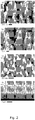
- Fig. 2 shows examples of four different silicon nanostructures obtainable using maskless RIE.
- a) and b) substrates are illustrated which have been metalized. Note the different scale bars.
- the nanostructure which is shown in Fig. 2a ) is a reproduction of the samples that have previously been demonstrated at DTU Nanotech.
- the side wall angle or taper of the nano-pillars could be controlled by adjusting the SF6:O2 ratio in the plasma to give more conical shaped peaks as illustrated by Fig. 2b ).
- the peak concentration could be controlled by adjusting the chamber pressure as illustrated by the resulting nanostructures shown in Fig. 2c ).
- SERS applications we found that both the shape and the density of the pillars are key variables.
- FIG. 3 Another exemplary embodiment of a SERS-active structure according to the invention in shown in FIG. 3 , illustrating SEM images of silicon nano-pillars a) before (tilted 70 °) and b) after metalization with 250 nm silver (tilted 45 °).
- a SERS-active structure includes a substrate and a plurality of nano-pillars disposed on a surface of the substrate. Each nano-pillar of the plurality of nano-pillars may extend from a surface of the substrate in a direction substantially perpendicular thereto.
- each nano-pillar may have a diameter different from the diameter of other nano-pillars, thereby providing nano-pillars of varying sizes.
- the nano-pillars are not arranged in rows and columns, or in an array, as are the nano-pillars of the SERS-active structure ( FIG. 1 ).
- the nano-pillars may be separated from adjacent nano-pillars by a distance that is within a predetermined range, some of the nano-pillars being spaced closer than others.
- the predetermined range may be between about 1 nm and about 5 ⁇ m, but is prefereably between about 1 and about 300 nanometers.
- the predetermined range may be selected to provide a range of distances that correspond to the size of various analyte molecules to be analyzed with the SERS-active structure, such that the molecules are capable of spanning between at least two adjacent nano-pillars.
- the height of the pillars (1.6 ⁇ m and 670 nm respectively) is a function of etching time.
- the side wall angles, inter peak distances and shape of the pillars appeared unaffected by prolonging the etch time.
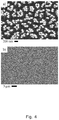
- Figure 4 illustrates SEM images using secondary electrons taken at a right angle to the surface.
- the silicon nanostructures could be produced uniformly over relatively large areas, Fig. 4b ). Neglecting edge effects, most of a 101.6 mm (4 inch) wafer ( ⁇ 28 cm 2 ) contains Raman enhancing area. Upscaling the process to larger wafers is believed achievable facilitating large scale fabrication of SERS surfaces.
- An exemplary method for making the SERS-active structure is one wherein a substrate may be provided including a wafer or die of, for example, silicon or germanium, or any other semiconductor material.
- an oxide layer is formed on or in a surface of the substrate.
- Various methods for forming an oxide layer on or in a surface of a substrate are known in the art of microdevice fabrication.
- a portion or portions of the oxide layer may be photolithographically removed to form regions of exposed silicon material of the underlying substrate.
- the oxide layer may be masked and etched to remove portions thereof.
- Each region of exposed silicon material may be disposed at the predetermined locations where the nano-pillars are to be formed.
- the regions of exposed silicon material may have substantially the same predetermined size and shape as the core of the nano-pillars. Alternatively, as is described further below, a more random pattern may also be obtained.
- nano-pillars are illustrated in FIGS. 2 and 4G as being of equal length and extending in parallel directions, the nano-pillars may have different lengths but will not extend in nonparallel directions relative to other nano-pillars.
- An exemplary SERS system may include one of the exemplary SERS-active structures, and may be used to perform surface enhanced Raman spectroscopy.
- the SERS system may include a sample or analyte stage, an excitation radiation source, and a detector.
- the analyte stage may include a SERS-active structure as described above.
- the SERS system also may include various optical components positioned between the excitation radiation source and the analyte stage, and various optical components positioned between the analyte stage and the detector.
- the excitation radiation source may include any suitable source for emitting radiation at the desired wavelength, and may be capable of emitting a tunable wavelength of radiation.
- any suitable source for emitting radiation at the desired wavelength and may be capable of emitting a tunable wavelength of radiation.
- commercially available semiconductor lasers, helium-neon lasers, carbon dioxide lasers, light emitting diodes, incandescent lamps, and many other known radiation emitting sources may be used as the excitation radiation source.
- the wavelengths that are emitted by the excitation radiation source may be any suitable wavelength for properly analyzing the analyte using SERS.
- An exemplary range of wavelengths that may be emitted by the excitation radiation source includes wavelengths between about 350 nm and about 1000 nm.
- the excitation radiation emitted by the source may be delivered either directly from the source to the analyte stage and the SERS-active structure.
- collimation, filtration, and subsequent focusing of the excitation radiation may be performed by optical components before the excitation radiation impinges on the analyte stage and the SERS-active structure.
- the SERS-active structure of the analyte stage may enhance the Raman signal of the analyte, as discussed previously.
- irradiation of the SERS-active structure by excitation radiation may increase the number photons inelastically scattered by an analyte molecule positioned near or adjacent to the SERS-active structure.
- the Raman scattered photons may be collimated, filtered, or focused with optical components.
- a filter or a plurality of filters may be employed, either as part of the structure of the detector, or as a separate unit that is configured to filter the wavelength of the excitation radiation, thus allowing only the Raman scattered photons to be received by the detector.
- the detector receives and detects the Raman scattered photons and may include a monochromator (or any other suitable device for determining the wavelength of the Raman scattered photons) and a device such as, for example, a photomultiplier for determining the quantity of Raman scattered photons (intensity).
- a monochromator or any other suitable device for determining the wavelength of the Raman scattered photons
- a device such as, for example, a photomultiplier for determining the quantity of Raman scattered photons (intensity).
- the Raman scattered photons are scattered isotropically, being scattered in all directions relative to the analyte stage.
- the position of the detector relative to the analyte stage is not particularly important.
- the detector may be positioned at, for example, an angle of 90.degree. relative to the direction of the incident excitation radiation to minimize the intensity of the incident excitation radiation that may be incident on the detector.
- a user may provide an analyte molecule or molecules adjacent to the SERS-active structure.
- the analyte and the SERS-active structure are irradiated with excitation radiation or light from the source. Raman scattered photons scattered by the analyte are then detected by the detector.
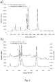
- FIG. 5 illustrates: a) The Raman spectrum of a 1 ⁇ L of 100 ⁇ M rhodamine 6G dropped onto the silver coated nanostructured surface shown in Fig. 3b ) and on a commercially available substrate (gold coated) using the same y-axis. b) For clarity the gold coated commercial substrate is plotted on a second y-axis. The spectra were obtained using 785 nm excitation with an integration time of 1 second.
- Figure 6 illustrates: a) The Raman spectrum of a self assembling monolayer of thiophenol on the silver coated nanostructured surface shown in Fig. 3b ) and on a commercially available substrate (gold coated) using the same y-axis. b) For clarity the commercial substrate is plotted on a second y-axis. The spectra were obtained using 785 nm excitation with an integration time of 0.5 seconds.
- the signal to noise ratio measured on the silver coated silicon nano-pillars shown in Fig. 4 is an improvement compared to the commercial substrate.
- the commercial substrate is a gold structure which is known to have a weaker Raman enhancement than silver.
- gold covered silicon nano-pillars are still two orders of magnitude better Raman enhancers (not shown here) than the commercial substrate.
- Relatively large areas ( ⁇ 28 cm 2 ) of uniform Raman enhancing surfaces can be routinely produced in a two-step process which takes no more than 20 minutes from start to finish of where most of this time is spent pumping to vacuum.
- the RIE process is narrowly controlled by the processing equipment hence enabling the tailoring of diverse silicon nanostructures as demonstrated in Fig. 2 .
- this technique is superior to current electron beam lithography defined surfaces in terms of cost and time and it is more reproducible than chemically deposited rough metal layers and metallic nanoparticle arrays.
- Hu et al. M. Hu, J. Tang, F.S. Ou, H.P. Kuo, S.-Y. Wang, Z. Li and R.S. Williams, "Metal coated Si nanograss as highly sensitive SERS sensors," Proceedings of the SPIE, vol. 7312 (1), 2009, pp. 73120I-73120I-6 ) report an enhancement factor of 6 x 10⁷ on silver coated silicon nanostructures very similar to those shown in Fig. 2c ).
- Hu also suggests that metal nanoparticles on the sides of the peaks are responsible for the observed Raman enhancement effect and is thus in agreement with the present observations.
- the conical peaks in Hu and Fig. 2c do not appear to be uniform in height. It is hypothesized that the present increase in enhancement factor compared to Hu can be attributed to the clustering enabled by the mechanical movement of the high aspect ratio vertical silicon nano-pillars shown in Fig. 4a ).
- the structures and systems disclosed herein may also be used to perform hyper-Raman spectroscopy.
- a very small number of photons may be scattered at frequencies corresponding to the higher order harmonics of the excitation radiation, such as the second and third harmonic generations (i.e., twice or three times the frequency of the excitation radiation).
- Some of these photons may have a frequency that is Raman-shifted relative to the frequencies corresponding to the higher order harmonics of the excitation radiation.
- These higher order Raman-scattered photons can provide information about the analyte molecule that cannot be obtained by first order Raman spectroscopy.
- Hyper-Raman spectroscopy involves the collection and analysis of these higher order Raman-scattered photons.
- the methods disclosed herein allow for the reproducible formation of SERS-active structures including nanoscale features having well controlled size, shape, location, and orientation. These structures allow for improved surface-enhanced Raman spectroscopy and may be used to produce molecular sensors having superior sensitivity relative to conventional SERS-active structures.
- the performance of nanoscale electronics, optoelectronics, molecular sensors, and other devices employing the Raman effect may be significantly improved by using the SERS-active structures disclosed herein.
- the methods disclosed herein allow for production of high quantities of SERS-active structures at relatively low cost.
Landscapes
- Health & Medical Sciences (AREA)
- Nuclear Medicine, Radiotherapy & Molecular Imaging (AREA)
- Physics & Mathematics (AREA)
- Life Sciences & Earth Sciences (AREA)
- Chemical & Material Sciences (AREA)
- Analytical Chemistry (AREA)
- Biochemistry (AREA)
- General Health & Medical Sciences (AREA)
- General Physics & Mathematics (AREA)
- Immunology (AREA)
- Pathology (AREA)
- Investigating, Analyzing Materials By Fluorescence Or Luminescence (AREA)
Applications Claiming Priority (2)
| Application Number | Priority Date | Filing Date | Title |
|---|---|---|---|
| DKPA200901149 | 2009-10-23 | ||
| PCT/DK2010/050284 WO2011047690A1 (en) | 2009-10-23 | 2010-10-25 | Surface enhanced raman scattering substrates consumables for raman spectroscopy |
Publications (2)
| Publication Number | Publication Date |
|---|---|
| EP2491372A1 EP2491372A1 (en) | 2012-08-29 |
| EP2491372B1 true EP2491372B1 (en) | 2021-07-21 |
Family
ID=43425815
Family Applications (1)
| Application Number | Title | Priority Date | Filing Date |
|---|---|---|---|
| EP10773237.2A Active EP2491372B1 (en) | 2009-10-23 | 2010-10-25 | Surface enhanced raman scattering substrates consumables for raman spectroscopy |
Country Status (4)
| Country | Link |
|---|---|
| US (1) | US8767202B2 (da) |
| EP (1) | EP2491372B1 (da) |
| DK (1) | DK2491372T3 (da) |
| WO (1) | WO2011047690A1 (da) |
Families Citing this family (67)
| Publication number | Priority date | Publication date | Assignee | Title |
|---|---|---|---|---|
| US9267894B2 (en) | 2012-08-10 | 2016-02-23 | Hamamatsu Photonics K.K. | Method for making surface enhanced Raman scattering device |
| EP2372348A1 (en) * | 2010-03-22 | 2011-10-05 | Imec | Methods and systems for surface enhanced optical detection |
| US8462333B2 (en) * | 2010-10-15 | 2013-06-11 | Hewlett-Packard Development Company, L.P. | Apparatus for performing SERS |
| US8477303B2 (en) * | 2011-01-26 | 2013-07-02 | Hewlett-Packard Development Company, L.P. | Reconfigurable surface enhanced Raman spectroscopy apparatus, system and method |
| US20120188539A1 (en) * | 2011-01-26 | 2012-07-26 | Stuke Michael J | Nanorod surface enhanced raman spectroscopy apparatus, system and method |
| US9310306B2 (en) * | 2011-02-17 | 2016-04-12 | Hewlett-Packard Development Company, L.P. | Apparatus for use in sensing applications |
| US8593629B2 (en) | 2011-02-17 | 2013-11-26 | Hewlett-Packard Development Company, L.P. | Apparatus for performing SERS |
| US8842265B2 (en) * | 2011-04-19 | 2014-09-23 | Hewlett-Packard Development Company, L.P. | Configurable grating based on collapsing nano-fingers |
| CN103620358B (zh) | 2011-05-20 | 2016-07-06 | 惠普发展公司,有限责任合伙企业 | 表面增强拉曼光谱传感器、传感系统和方法 |
| US8848183B2 (en) * | 2011-07-22 | 2014-09-30 | Hewlett-Packard Development Company, L.P. | Apparatus having nano-fingers of different physical characteristics |
| US9377409B2 (en) | 2011-07-29 | 2016-06-28 | Hewlett-Packard Development Company, L.P. | Fabricating an apparatus for use in a sensing application |
| US20140218727A1 (en) * | 2011-10-26 | 2014-08-07 | Zhiyong Li | Apparatus for use in a sensing application having a destructible cover |
| JP5848458B2 (ja) | 2011-10-27 | 2016-01-27 | ヒューレット−パッカード デベロップメント カンパニー エル.ピー.Hewlett‐Packard Development Company, L.P. | 化学種をフィルタリングする装置 |
| WO2013119228A1 (en) | 2012-02-08 | 2013-08-15 | Hewlett-Packard Development Company, L.P. | Gas-phase delivery system for molecule sensing apparatus |
| US9574990B2 (en) * | 2012-02-28 | 2017-02-21 | Hewlett-Packard Development Company, L.P. | SERS structures with nanoporous materials |
| US8994937B2 (en) * | 2012-04-18 | 2015-03-31 | Hewlett-Packard Development Company, L.P. | Surface enhanced Raman spectroscopy calibration curve generating systems |
| US9453793B2 (en) | 2012-04-20 | 2016-09-27 | Hewlett-Packard Development Company, L.P. | Integrated sensors |
| DK2839295T3 (da) | 2012-04-20 | 2017-05-15 | Hewlett-Packard Dev Company | Integrerede sensorer |
| CN104541158B (zh) | 2012-08-10 | 2017-05-24 | 浜松光子学株式会社 | 表面增强拉曼散射元件、以及制造表面增强拉曼散射元件的方法 |
| JP6151948B2 (ja) | 2013-03-29 | 2017-06-21 | 浜松ホトニクス株式会社 | 表面増強ラマン散乱ユニット及びラマン分光分析方法 |
| JP6055234B2 (ja) | 2012-08-10 | 2016-12-27 | 浜松ホトニクス株式会社 | 表面増強ラマン散乱ユニット |
| CN104508466B (zh) * | 2012-08-10 | 2018-07-17 | 浜松光子学株式会社 | 表面增强拉曼散射元件 |
| CN108827928B (zh) | 2012-08-10 | 2021-12-24 | 浜松光子学株式会社 | 表面增强拉曼散射单元及其使用方法 |
| JP6023669B2 (ja) * | 2013-07-05 | 2016-11-09 | 浜松ホトニクス株式会社 | 表面増強ラマン散乱素子 |
| JP6058313B2 (ja) | 2012-08-10 | 2017-01-11 | 浜松ホトニクス株式会社 | 表面増強ラマン散乱ユニット |
| JP5908370B2 (ja) * | 2012-08-10 | 2016-04-26 | 浜松ホトニクス株式会社 | 表面増強ラマン散乱ユニット |
| JP5945192B2 (ja) | 2012-08-10 | 2016-07-05 | 浜松ホトニクス株式会社 | 表面増強ラマン散乱ユニット |
| CN104520696B (zh) | 2012-08-10 | 2018-01-12 | 浜松光子学株式会社 | 表面增强拉曼散射元件及其制造方法 |
| JP5921380B2 (ja) | 2012-08-10 | 2016-05-24 | 浜松ホトニクス株式会社 | 表面増強ラマン散乱ユニット |
| JP6230250B2 (ja) | 2013-03-29 | 2017-11-15 | 浜松ホトニクス株式会社 | 表面増強ラマン散乱ユニット、及びラマン分光分析方法 |
| EP4033222A1 (en) | 2012-08-10 | 2022-07-27 | Hamamatsu Photonics K.K. | Surface-enhanced raman scattering unit |
| JP5921381B2 (ja) | 2012-08-10 | 2016-05-24 | 浜松ホトニクス株式会社 | 表面増強ラマン散乱ユニット |
| JP6023509B2 (ja) | 2012-08-10 | 2016-11-09 | 浜松ホトニクス株式会社 | 表面増強ラマン散乱ユニット |
| US10633734B2 (en) | 2012-10-05 | 2020-04-28 | California Institute Of Technology | Optical sensor for analyte detection |
| WO2014055951A1 (en) * | 2012-10-05 | 2014-04-10 | California Institute Of Technology | Optical sensor for analyte detection |
| AU2013358894A1 (en) * | 2012-12-13 | 2015-07-02 | California Institute Of Technology | Fabrication of three-dimensional high surface area electrodes |
| US9476833B2 (en) * | 2013-01-30 | 2016-10-25 | Hewlett-Packard Devleopment Company, L.P. | Forming 3-D nano-particle assemblies |
| MX2015010152A (es) | 2013-02-06 | 2015-12-16 | California Inst Of Techn | Dispositivos implantables, miniaturizados de sensor electroquimico. |
| US20160003732A1 (en) * | 2013-03-14 | 2016-01-07 | Hewlett-Packard Development Company, L.P. | Devices to detect a substance and methods of producing such a device |
| TWI611175B (zh) | 2013-03-29 | 2018-01-11 | Hamamatsu Photonics Kk | 表面增強拉曼散射單元及拉曼分光分析方法 |
| US9778197B2 (en) * | 2013-08-05 | 2017-10-03 | Lawrence Livermore National Security, Llc | Metal-dielectric-CNT nanowires for surface-enhanced Raman spectroscopy |
| KR101448111B1 (ko) * | 2013-09-17 | 2014-10-13 | 한국기계연구원 | 표면 증강 라만 분광용 기판 및 이의 제조방법 |
| WO2015123457A1 (en) | 2014-02-12 | 2015-08-20 | California Institute Of Technology | Plasmonics nanostructures for multiplexing implantable sensors |
| WO2015123461A1 (en) * | 2014-02-12 | 2015-08-20 | California Institute Of Technology | Reflowed gold nanostructures for surface enhanced raman spectroscopy |
| JP6544504B2 (ja) * | 2014-05-07 | 2019-07-17 | セイコーエプソン株式会社 | 分析装置及び電子機器 |
| US10085646B2 (en) | 2014-05-26 | 2018-10-02 | Board Of Supervisors Of Louisiana State University And Agricultural And Mechanical College | Contact-type endoscope SERS probe, and related methods |
| US9846125B2 (en) * | 2014-09-05 | 2017-12-19 | California Institute Of Technology | Surface enhanced Raman spectroscopy detection of gases, particles and liquids through nanopillar structures |
| WO2016036410A1 (en) | 2014-09-05 | 2016-03-10 | California Institute Of Technology | Multiplexed surface enhanced raman sensors for early disease detection and in-situ bacterial monitoring |
| WO2016041842A1 (en) | 2014-09-17 | 2016-03-24 | Danmarks Tekniske Universitet | Method and system of detecting a target analyte |
| US9512000B2 (en) | 2014-12-09 | 2016-12-06 | California Institute Of Technology | Fabrication and self-aligned local functionalization of nanocups and various plasmonic nanostructures on flexible substrates for implantable and sensing applications |
| EP3076161A1 (en) | 2015-04-01 | 2016-10-05 | Danmarks Tekniske Universitet | A substrate and a method of using it |
| US10368788B2 (en) | 2015-07-23 | 2019-08-06 | California Institute Of Technology | System and methods for wireless drug delivery on command |
| TW201725385A (zh) * | 2016-01-05 | 2017-07-16 | 財團法人工業技術研究院 | 具有薄層層析之拉曼檢測晶片及分離檢測分析物之方法 |
| CN108603837B (zh) | 2016-04-21 | 2021-07-06 | 惠普发展公司,有限责任合伙企业 | Sels纳米指状物侧壁涂层 |
| WO2018143930A1 (en) * | 2017-01-31 | 2018-08-09 | Hewlett-Packard Development Company, L.P. | Surface enhanced luminescence sensor nano finger |
| KR101914986B1 (ko) * | 2017-04-18 | 2019-01-31 | 한국기계연구원 | 분광분석용 기판 및 이의 제조방법 |
| CN108931515B (zh) | 2017-05-25 | 2023-09-15 | 三星电子株式会社 | 感测用基底和制造感测用基底的方法 |
| WO2019017939A1 (en) | 2017-07-19 | 2019-01-24 | Hewlett-Packard Development Company, L.P. | SPECTROSCOPIC DEVICE COMPRISING DESIGN GROUPS |
| CN108257865A (zh) * | 2018-01-17 | 2018-07-06 | 中国科学院物理研究所 | 低密度分立硅锥的无掩膜制备方法和所制备的分立硅锥 |
| TWI686599B (zh) * | 2018-05-24 | 2020-03-01 | 國立清華大學 | 塵蟎抗原檢測系統及方法 |
| US20220091041A1 (en) * | 2019-03-20 | 2022-03-24 | University Of Louisville Research Foundation, Inc. | Nanowire array for use with raman spectroscopy |
| US10900906B2 (en) | 2019-06-05 | 2021-01-26 | International Business Machines Corporation | Surface enhanced Raman scattering substrate |
| CN110108697B (zh) * | 2019-06-25 | 2022-03-08 | 北威(重庆)科技股份有限公司 | 表面增强拉曼散射微纳芯片及其制备方法、应用和拉曼光谱测试系统 |
| CN111879753B (zh) * | 2020-08-05 | 2023-07-04 | 山东寿光检测集团有限公司 | 用于检测新型冠状病毒的贵金属纳米锥sers衬底及制备方法 |
| CN114113034A (zh) * | 2021-11-17 | 2022-03-01 | 肇庆市华师大光电产业研究院 | 一种多壁碳纳米管“手指”的制备方法及其在表面增强拉曼散射检测中的应用 |
| CN115287606A (zh) * | 2022-07-29 | 2022-11-04 | 中国科学院西安光学精密机械研究所 | 一种基于黑硅的表面增强拉曼光谱基底制备方法 |
| CN120352408B (zh) * | 2025-04-22 | 2026-04-10 | 常州工程职业技术学院 | 一种基于针尖硅片的复合sers基底及其制备方法和应用 |
Citations (1)
| Publication number | Priority date | Publication date | Assignee | Title |
|---|---|---|---|---|
| US20080024776A1 (en) * | 2006-07-25 | 2008-01-31 | Alexandre Bratkovski | Controllable surface enhanced Raman spectroscopy |
Family Cites Families (28)
| Publication number | Priority date | Publication date | Assignee | Title |
|---|---|---|---|---|
| US5017007A (en) * | 1989-07-27 | 1991-05-21 | Milne Christopher G | Apparatus and microbase for surface-enhanced raman spectroscopy system and method for producing same |
| WO1999044045A1 (en) | 1998-02-27 | 1999-09-02 | Massachusetts Institute Of Technology | Single molecule detection with surface-enhanced raman scattering and applications in dna or rna sequencing |
| US7192778B2 (en) * | 1999-10-06 | 2007-03-20 | Natan Michael J | Surface enhanced spectroscopy-active composite nanoparticles |
| US6623977B1 (en) * | 1999-11-05 | 2003-09-23 | Real-Time Analyzers, Inc. | Material for surface-enhanced Raman spectroscopy, and SER sensors and method for preparing same |
| US6970239B2 (en) * | 2002-06-12 | 2005-11-29 | Intel Corporation | Metal coated nanocrystalline silicon as an active surface enhanced Raman spectroscopy (SERS) substrate |
| US6989897B2 (en) * | 2002-06-12 | 2006-01-24 | Intel Corporation | Metal coated nanocrystalline silicon as an active surface enhanced Raman spectroscopy (SERS) substrate |
| US7163659B2 (en) * | 2002-12-03 | 2007-01-16 | Hewlett-Packard Development Company, L.P. | Free-standing nanowire sensor and method for detecting an analyte in a fluid |
| US7460224B2 (en) * | 2005-12-19 | 2008-12-02 | Opto Trace Technologies, Inc. | Arrays of nano structures for surface-enhanced Raman scattering |
| US20050147963A1 (en) * | 2003-12-29 | 2005-07-07 | Intel Corporation | Composite organic-inorganic nanoparticles and methods for use thereof |
| US8048377B1 (en) * | 2004-03-08 | 2011-11-01 | Hewlett-Packard Development Company, L.P. | Immobilizing chemical or biological sensing molecules on semi-conducting nanowires |
| US7321422B2 (en) * | 2004-09-16 | 2008-01-22 | Hewlett-Packard Development Company, L.P. | SERS-active structures having nanoscale dimensions |
| US7158219B2 (en) * | 2004-09-16 | 2007-01-02 | Hewlett-Packard Development Company, L.P. | SERS-active structures including nanowires |
| CN101057132B (zh) * | 2004-11-04 | 2012-04-18 | 雷尼绍诊断有限公司 | 用于增强的拉曼光谱学的金属纳米孔光子晶体 |
| US7236242B2 (en) * | 2005-01-27 | 2007-06-26 | Hewlett-Packard Development Company, L.P. | Nano-enhanced Raman spectroscopy-active nanostructures including elongated components and methods of making the same |
| US7651863B2 (en) * | 2005-07-14 | 2010-01-26 | 3M Innovative Properties Company | Surface-enhanced spectroscopic method, flexible structured substrate, and method of making the same |
| US7426025B2 (en) * | 2005-09-23 | 2008-09-16 | Hewlett-Packard Development Company, L.P. | Nanostructures, systems, and methods including nanolasers for enhanced Raman spectroscopy |
| US7342656B2 (en) * | 2005-10-17 | 2008-03-11 | Hewlett-Packard Development Company, L.P. | Dynamically variable separation among nanoparticles for nano-enhanced Raman spectroscopy (NERS) molecular sensing |
| WO2007059514A2 (en) * | 2005-11-15 | 2007-05-24 | Oxonica, Inc. | Sers-based methods for detection of bioagents |
| US7388661B2 (en) * | 2006-10-20 | 2008-06-17 | Hewlett-Packard Development Company, L.P. | Nanoscale structures, systems, and methods for use in nano-enhanced raman spectroscopy (NERS) |
| US7727776B2 (en) * | 2006-10-24 | 2010-06-01 | Honeywell International Inc. | Core-shell nanoparticles for detection based on SERS |
| US7898658B2 (en) * | 2007-01-23 | 2011-03-01 | The Regents Of The University Of California | Platform for chemical and biological sensing by surface-enhanced Raman spectroscopy |
| DE102007037201B4 (de) * | 2007-07-31 | 2010-09-16 | Technische Universität Dresden | Element zur oberflächenverstärkten Spektroskopie und Verfahren zur Herstellung des Elements sowie seine Verwendung |
| DE102007037020B3 (de) | 2007-08-06 | 2008-08-21 | MAX-PLANCK-Gesellschaft zur Förderung der Wissenschaften e.V. | Avalanche-Photodiode |
| US8115920B2 (en) * | 2007-11-14 | 2012-02-14 | 3M Innovative Properties Company | Method of making microarrays |
| US20090218028A1 (en) * | 2008-02-29 | 2009-09-03 | Honeywell International Inc. | Aligned surface-enhanced raman scattering particles, coatings made thereby, and methods of using same |
| US7960252B2 (en) * | 2008-09-30 | 2011-06-14 | Yung-Tin Chen | Method for forming a semiconductor film including a film forming gas and decomposing gas while emitting a laser sheet |
| US8427639B2 (en) * | 2009-05-07 | 2013-04-23 | Nant Holdings Ip, Llc | Surfaced enhanced Raman spectroscopy substrates |
| US8223331B2 (en) * | 2009-06-19 | 2012-07-17 | Hewlett-Packard Development Company, L.P. | Signal-amplification device for surface enhanced raman spectroscopy |
-
2010
- 2010-10-25 WO PCT/DK2010/050284 patent/WO2011047690A1/en not_active Ceased
- 2010-10-25 US US12/911,061 patent/US8767202B2/en active Active
- 2010-10-25 EP EP10773237.2A patent/EP2491372B1/en active Active
- 2010-10-25 DK DK10773237.2T patent/DK2491372T3/da active
Patent Citations (1)
| Publication number | Priority date | Publication date | Assignee | Title |
|---|---|---|---|---|
| US20080024776A1 (en) * | 2006-07-25 | 2008-01-31 | Alexandre Bratkovski | Controllable surface enhanced Raman spectroscopy |
Also Published As
| Publication number | Publication date |
|---|---|
| WO2011047690A1 (en) | 2011-04-28 |
| DK2491372T3 (da) | 2021-10-18 |
| EP2491372A1 (en) | 2012-08-29 |
| US20110116089A1 (en) | 2011-05-19 |
| US8767202B2 (en) | 2014-07-01 |
Similar Documents
| Publication | Publication Date | Title |
|---|---|---|
| EP2491372B1 (en) | Surface enhanced raman scattering substrates consumables for raman spectroscopy | |
| US7158219B2 (en) | SERS-active structures including nanowires | |
| US7236242B2 (en) | Nano-enhanced Raman spectroscopy-active nanostructures including elongated components and methods of making the same | |
| US7388661B2 (en) | Nanoscale structures, systems, and methods for use in nano-enhanced raman spectroscopy (NERS) | |
| US9909989B2 (en) | Structures for enhancement of local electric field, light absorption, light radiation, material detection and methods for making and using of the same | |
| US7511808B2 (en) | Analyte stages including tunable resonant cavities and Raman signal-enhancing structures | |
| US7321422B2 (en) | SERS-active structures having nanoscale dimensions | |
| EP1541994B1 (en) | Microstructure for use in raman spectrometry and production process for the microstructure | |
| CN101057132B (zh) | 用于增强的拉曼光谱学的金属纳米孔光子晶体 | |
| US7397558B2 (en) | Ordered array of nanoparticles for efficient nanoenhanced Raman scattering detection and methods of forming the same | |
| US20060146323A1 (en) | Nanowires for surface-enhanced raman scattering molecular sensors | |
| US20090033929A1 (en) | Substrates for raman spectroscopy having discontinuous metal coatings | |
| WO2008018907A2 (en) | Nanowire heterostructures, methods of forming the same and their enhanced raman activity | |
| US20130115413A1 (en) | Fabrication and use of elevated optical nanoantennas | |
| JP2008512668A (ja) | ラマン分光法 | |
| JP7598614B2 (ja) | ラマン分光測定装置、ラマン分光測定方法および表面増強ラマン散乱デバイス | |
| US20080093217A1 (en) | Method for arranging nanoparticles by way of an electric field, structures and systems therefor | |
| Schmidt et al. | Towards easily reproducible nano-structured SERS substrates | |
| US7309642B2 (en) | Metallic quantum dots fabricated by a superlattice structure | |
| Schmidt et al. | Metal-coated silicon nanopillars with large Raman enhancement for explosives detection | |
| KR20160037852A (ko) | 무기물-금속 구조체가 형성된 기판 및 이의 제조방법 | |
| JP2010066060A (ja) | レーザ脱離イオン化質量分析方法およびそれに用いられる質量分析用基板 |
Legal Events
| Date | Code | Title | Description |
|---|---|---|---|
| PUAI | Public reference made under article 153(3) epc to a published international application that has entered the european phase |
Free format text: ORIGINAL CODE: 0009012 |
|
| 17P | Request for examination filed |
Effective date: 20120523 |
|
| AK | Designated contracting states |
Kind code of ref document: A1 Designated state(s): AL AT BE BG CH CY CZ DE DK EE ES FI FR GB GR HR HU IE IS IT LI LT LU LV MC MK MT NL NO PL PT RO RS SE SI SK SM TR |
|
| DAX | Request for extension of the european patent (deleted) | ||
| RAP1 | Party data changed (applicant data changed or rights of an application transferred) |
Owner name: DANMARKS TEKNISKE UNIVERSITET |
|
| STAA | Information on the status of an ep patent application or granted ep patent |
Free format text: STATUS: EXAMINATION IS IN PROGRESS |
|
| 17Q | First examination report despatched |
Effective date: 20180529 |
|
| GRAP | Despatch of communication of intention to grant a patent |
Free format text: ORIGINAL CODE: EPIDOSNIGR1 |
|
| STAA | Information on the status of an ep patent application or granted ep patent |
Free format text: STATUS: GRANT OF PATENT IS INTENDED |
|
| INTG | Intention to grant announced |
Effective date: 20200810 |
|
| GRAS | Grant fee paid |
Free format text: ORIGINAL CODE: EPIDOSNIGR3 |
|
| GRAJ | Information related to disapproval of communication of intention to grant by the applicant or resumption of examination proceedings by the epo deleted |
Free format text: ORIGINAL CODE: EPIDOSDIGR1 |
|
| GRAL | Information related to payment of fee for publishing/printing deleted |
Free format text: ORIGINAL CODE: EPIDOSDIGR3 |
|
| STAA | Information on the status of an ep patent application or granted ep patent |
Free format text: STATUS: EXAMINATION IS IN PROGRESS |
|
| GRAP | Despatch of communication of intention to grant a patent |
Free format text: ORIGINAL CODE: EPIDOSNIGR1 |
|
| INTC | Intention to grant announced (deleted) | ||
| STAA | Information on the status of an ep patent application or granted ep patent |
Free format text: STATUS: GRANT OF PATENT IS INTENDED |
|
| INTG | Intention to grant announced |
Effective date: 20210128 |
|
| GRAA | (expected) grant |
Free format text: ORIGINAL CODE: 0009210 |
|
| STAA | Information on the status of an ep patent application or granted ep patent |
Free format text: STATUS: THE PATENT HAS BEEN GRANTED |
|
| RAP3 | Party data changed (applicant data changed or rights of an application transferred) |
Owner name: DANMARKS TEKNISKE UNIVERSITET |
|
| AK | Designated contracting states |
Kind code of ref document: B1 Designated state(s): AL AT BE BG CH CY CZ DE DK EE ES FI FR GB GR HR HU IE IS IT LI LT LU LV MC MK MT NL NO PL PT RO RS SE SI SK SM TR |
|
| REG | Reference to a national code |
Ref country code: GB Ref legal event code: FG4D |
|
| REG | Reference to a national code |
Ref country code: CH Ref legal event code: EP |
|
| REG | Reference to a national code |
Ref country code: DE Ref legal event code: R096 Ref document number: 602010067303 Country of ref document: DE |
|
| REG | Reference to a national code |
Ref country code: AT Ref legal event code: REF Ref document number: 1413020 Country of ref document: AT Kind code of ref document: T Effective date: 20210815 |
|
| REG | Reference to a national code |
Ref country code: IE Ref legal event code: FG4D |
|
| REG | Reference to a national code |
Ref country code: DK Ref legal event code: T3 Effective date: 20211012 |
|
| REG | Reference to a national code |
Ref country code: LT Ref legal event code: MG9D |
|
| REG | Reference to a national code |
Ref country code: NL Ref legal event code: MP Effective date: 20210721 |
|
| REG | Reference to a national code |
Ref country code: AT Ref legal event code: MK05 Ref document number: 1413020 Country of ref document: AT Kind code of ref document: T Effective date: 20210721 |
|
| PG25 | Lapsed in a contracting state [announced via postgrant information from national office to epo] |
Ref country code: HR Free format text: LAPSE BECAUSE OF FAILURE TO SUBMIT A TRANSLATION OF THE DESCRIPTION OR TO PAY THE FEE WITHIN THE PRESCRIBED TIME-LIMIT Effective date: 20210721 Ref country code: SE Free format text: LAPSE BECAUSE OF FAILURE TO SUBMIT A TRANSLATION OF THE DESCRIPTION OR TO PAY THE FEE WITHIN THE PRESCRIBED TIME-LIMIT Effective date: 20210721 Ref country code: NL Free format text: LAPSE BECAUSE OF FAILURE TO SUBMIT A TRANSLATION OF THE DESCRIPTION OR TO PAY THE FEE WITHIN THE PRESCRIBED TIME-LIMIT Effective date: 20210721 Ref country code: RS Free format text: LAPSE BECAUSE OF FAILURE TO SUBMIT A TRANSLATION OF THE DESCRIPTION OR TO PAY THE FEE WITHIN THE PRESCRIBED TIME-LIMIT Effective date: 20210721 Ref country code: PT Free format text: LAPSE BECAUSE OF FAILURE TO SUBMIT A TRANSLATION OF THE DESCRIPTION OR TO PAY THE FEE WITHIN THE PRESCRIBED TIME-LIMIT Effective date: 20211122 Ref country code: NO Free format text: LAPSE BECAUSE OF FAILURE TO SUBMIT A TRANSLATION OF THE DESCRIPTION OR TO PAY THE FEE WITHIN THE PRESCRIBED TIME-LIMIT Effective date: 20211021 Ref country code: ES Free format text: LAPSE BECAUSE OF FAILURE TO SUBMIT A TRANSLATION OF THE DESCRIPTION OR TO PAY THE FEE WITHIN THE PRESCRIBED TIME-LIMIT Effective date: 20210721 Ref country code: FI Free format text: LAPSE BECAUSE OF FAILURE TO SUBMIT A TRANSLATION OF THE DESCRIPTION OR TO PAY THE FEE WITHIN THE PRESCRIBED TIME-LIMIT Effective date: 20210721 Ref country code: LT Free format text: LAPSE BECAUSE OF FAILURE TO SUBMIT A TRANSLATION OF THE DESCRIPTION OR TO PAY THE FEE WITHIN THE PRESCRIBED TIME-LIMIT Effective date: 20210721 Ref country code: AT Free format text: LAPSE BECAUSE OF FAILURE TO SUBMIT A TRANSLATION OF THE DESCRIPTION OR TO PAY THE FEE WITHIN THE PRESCRIBED TIME-LIMIT Effective date: 20210721 Ref country code: BG Free format text: LAPSE BECAUSE OF FAILURE TO SUBMIT A TRANSLATION OF THE DESCRIPTION OR TO PAY THE FEE WITHIN THE PRESCRIBED TIME-LIMIT Effective date: 20211021 |
|
| PG25 | Lapsed in a contracting state [announced via postgrant information from national office to epo] |
Ref country code: PL Free format text: LAPSE BECAUSE OF FAILURE TO SUBMIT A TRANSLATION OF THE DESCRIPTION OR TO PAY THE FEE WITHIN THE PRESCRIBED TIME-LIMIT Effective date: 20210721 Ref country code: LV Free format text: LAPSE BECAUSE OF FAILURE TO SUBMIT A TRANSLATION OF THE DESCRIPTION OR TO PAY THE FEE WITHIN THE PRESCRIBED TIME-LIMIT Effective date: 20210721 Ref country code: GR Free format text: LAPSE BECAUSE OF FAILURE TO SUBMIT A TRANSLATION OF THE DESCRIPTION OR TO PAY THE FEE WITHIN THE PRESCRIBED TIME-LIMIT Effective date: 20211022 |
|
| RAP4 | Party data changed (patent owner data changed or rights of a patent transferred) |
Owner name: DANMARKS TEKNISKE UNIVERSITET |
|
| REG | Reference to a national code |
Ref country code: DE Ref legal event code: R097 Ref document number: 602010067303 Country of ref document: DE |
|
| PLBE | No opposition filed within time limit |
Free format text: ORIGINAL CODE: 0009261 |
|
| STAA | Information on the status of an ep patent application or granted ep patent |
Free format text: STATUS: NO OPPOSITION FILED WITHIN TIME LIMIT |
|
| REG | Reference to a national code |
Ref country code: CH Ref legal event code: PL |
|
| PG25 | Lapsed in a contracting state [announced via postgrant information from national office to epo] |
Ref country code: SM Free format text: LAPSE BECAUSE OF FAILURE TO SUBMIT A TRANSLATION OF THE DESCRIPTION OR TO PAY THE FEE WITHIN THE PRESCRIBED TIME-LIMIT Effective date: 20210721 Ref country code: SK Free format text: LAPSE BECAUSE OF FAILURE TO SUBMIT A TRANSLATION OF THE DESCRIPTION OR TO PAY THE FEE WITHIN THE PRESCRIBED TIME-LIMIT Effective date: 20210721 Ref country code: RO Free format text: LAPSE BECAUSE OF FAILURE TO SUBMIT A TRANSLATION OF THE DESCRIPTION OR TO PAY THE FEE WITHIN THE PRESCRIBED TIME-LIMIT Effective date: 20210721 Ref country code: EE Free format text: LAPSE BECAUSE OF FAILURE TO SUBMIT A TRANSLATION OF THE DESCRIPTION OR TO PAY THE FEE WITHIN THE PRESCRIBED TIME-LIMIT Effective date: 20210721 Ref country code: CZ Free format text: LAPSE BECAUSE OF FAILURE TO SUBMIT A TRANSLATION OF THE DESCRIPTION OR TO PAY THE FEE WITHIN THE PRESCRIBED TIME-LIMIT Effective date: 20210721 Ref country code: AL Free format text: LAPSE BECAUSE OF FAILURE TO SUBMIT A TRANSLATION OF THE DESCRIPTION OR TO PAY THE FEE WITHIN THE PRESCRIBED TIME-LIMIT Effective date: 20210721 |
|
| REG | Reference to a national code |
Ref country code: BE Ref legal event code: MM Effective date: 20211031 |
|
| 26N | No opposition filed |
Effective date: 20220422 |
|
| PG25 | Lapsed in a contracting state [announced via postgrant information from national office to epo] |
Ref country code: MC Free format text: LAPSE BECAUSE OF FAILURE TO SUBMIT A TRANSLATION OF THE DESCRIPTION OR TO PAY THE FEE WITHIN THE PRESCRIBED TIME-LIMIT Effective date: 20210721 |
|
| PG25 | Lapsed in a contracting state [announced via postgrant information from national office to epo] |
Ref country code: LU Free format text: LAPSE BECAUSE OF NON-PAYMENT OF DUE FEES Effective date: 20211025 Ref country code: IT Free format text: LAPSE BECAUSE OF FAILURE TO SUBMIT A TRANSLATION OF THE DESCRIPTION OR TO PAY THE FEE WITHIN THE PRESCRIBED TIME-LIMIT Effective date: 20210721 Ref country code: BE Free format text: LAPSE BECAUSE OF NON-PAYMENT OF DUE FEES Effective date: 20211031 |
|
| PG25 | Lapsed in a contracting state [announced via postgrant information from national office to epo] |
Ref country code: LI Free format text: LAPSE BECAUSE OF NON-PAYMENT OF DUE FEES Effective date: 20211031 Ref country code: CH Free format text: LAPSE BECAUSE OF NON-PAYMENT OF DUE FEES Effective date: 20211031 |
|
| PG25 | Lapsed in a contracting state [announced via postgrant information from national office to epo] |
Ref country code: IE Free format text: LAPSE BECAUSE OF NON-PAYMENT OF DUE FEES Effective date: 20211025 |
|
| PG25 | Lapsed in a contracting state [announced via postgrant information from national office to epo] |
Ref country code: HU Free format text: LAPSE BECAUSE OF FAILURE TO SUBMIT A TRANSLATION OF THE DESCRIPTION OR TO PAY THE FEE WITHIN THE PRESCRIBED TIME-LIMIT; INVALID AB INITIO Effective date: 20101025 Ref country code: CY Free format text: LAPSE BECAUSE OF FAILURE TO SUBMIT A TRANSLATION OF THE DESCRIPTION OR TO PAY THE FEE WITHIN THE PRESCRIBED TIME-LIMIT Effective date: 20210721 |
|
| P01 | Opt-out of the competence of the unified patent court (upc) registered |
Effective date: 20230503 |
|
| PG25 | Lapsed in a contracting state [announced via postgrant information from national office to epo] |
Ref country code: MK Free format text: LAPSE BECAUSE OF FAILURE TO SUBMIT A TRANSLATION OF THE DESCRIPTION OR TO PAY THE FEE WITHIN THE PRESCRIBED TIME-LIMIT Effective date: 20210721 |
|
| PG25 | Lapsed in a contracting state [announced via postgrant information from national office to epo] |
Ref country code: TR Free format text: LAPSE BECAUSE OF FAILURE TO SUBMIT A TRANSLATION OF THE DESCRIPTION OR TO PAY THE FEE WITHIN THE PRESCRIBED TIME-LIMIT Effective date: 20210721 |
|
| PG25 | Lapsed in a contracting state [announced via postgrant information from national office to epo] |
Ref country code: MT Free format text: LAPSE BECAUSE OF FAILURE TO SUBMIT A TRANSLATION OF THE DESCRIPTION OR TO PAY THE FEE WITHIN THE PRESCRIBED TIME-LIMIT Effective date: 20210721 |
|
| PGFP | Annual fee paid to national office [announced via postgrant information from national office to epo] |
Ref country code: GB Payment date: 20250904 Year of fee payment: 16 |
|
| PGFP | Annual fee paid to national office [announced via postgrant information from national office to epo] |
Ref country code: FR Payment date: 20250908 Year of fee payment: 16 |
|
| PGFP | Annual fee paid to national office [announced via postgrant information from national office to epo] |
Ref country code: DE Payment date: 20250902 Year of fee payment: 16 |
|
| PGFP | Annual fee paid to national office [announced via postgrant information from national office to epo] |
Ref country code: DK Payment date: 20251014 Year of fee payment: 16 |