EP2492952A2 - Lichtemittierende Vorrichtung auf Nitridbasis mit hervorragender Kristallinität und Helligkeit und Verfahren zu ihrer Herstellung - Google Patents
Lichtemittierende Vorrichtung auf Nitridbasis mit hervorragender Kristallinität und Helligkeit und Verfahren zu ihrer Herstellung Download PDFInfo
- Publication number
- EP2492952A2 EP2492952A2 EP11167413A EP11167413A EP2492952A2 EP 2492952 A2 EP2492952 A2 EP 2492952A2 EP 11167413 A EP11167413 A EP 11167413A EP 11167413 A EP11167413 A EP 11167413A EP 2492952 A2 EP2492952 A2 EP 2492952A2
- Authority
- EP
- European Patent Office
- Prior art keywords
- nitride
- layer
- light emitting
- growth
- type
- Prior art date
- Legal status (The legal status is an assumption and is not a legal conclusion. Google has not performed a legal analysis and makes no representation as to the accuracy of the status listed.)
- Withdrawn
Links
Images
Classifications
-
- H—ELECTRICITY
- H10—SEMICONDUCTOR DEVICES; ELECTRIC SOLID-STATE DEVICES NOT OTHERWISE PROVIDED FOR
- H10H—INORGANIC LIGHT-EMITTING SEMICONDUCTOR DEVICES HAVING POTENTIAL BARRIERS
- H10H20/00—Individual inorganic light-emitting semiconductor devices having potential barriers, e.g. light-emitting diodes [LED]
- H10H20/80—Constructional details
- H10H20/81—Bodies
- H10H20/819—Bodies characterised by their shape, e.g. curved or truncated substrates
- H10H20/82—Roughened surfaces, e.g. at the interface between epitaxial layers
-
- H—ELECTRICITY
- H10—SEMICONDUCTOR DEVICES; ELECTRIC SOLID-STATE DEVICES NOT OTHERWISE PROVIDED FOR
- H10P—GENERIC PROCESSES OR APPARATUS FOR THE MANUFACTURE OR TREATMENT OF DEVICES COVERED BY CLASS H10
- H10P14/00—Formation of materials, e.g. in the shape of layers or pillars
- H10P14/20—Formation of materials, e.g. in the shape of layers or pillars of semiconductor materials
- H10P14/32—Formation of materials, e.g. in the shape of layers or pillars of semiconductor materials characterised by intermediate layers between substrates and deposited layers
- H10P14/3242—Structure
- H10P14/3256—Microstructure
-
- H—ELECTRICITY
- H10—SEMICONDUCTOR DEVICES; ELECTRIC SOLID-STATE DEVICES NOT OTHERWISE PROVIDED FOR
- H10H—INORGANIC LIGHT-EMITTING SEMICONDUCTOR DEVICES HAVING POTENTIAL BARRIERS
- H10H20/00—Individual inorganic light-emitting semiconductor devices having potential barriers, e.g. light-emitting diodes [LED]
- H10H20/01—Manufacture or treatment
- H10H20/011—Manufacture or treatment of bodies, e.g. forming semiconductor layers
- H10H20/013—Manufacture or treatment of bodies, e.g. forming semiconductor layers having light-emitting regions comprising only Group III-V materials
- H10H20/0133—Manufacture or treatment of bodies, e.g. forming semiconductor layers having light-emitting regions comprising only Group III-V materials with a substrate not being Group III-V materials
- H10H20/01335—Manufacture or treatment of bodies, e.g. forming semiconductor layers having light-emitting regions comprising only Group III-V materials with a substrate not being Group III-V materials the light-emitting regions comprising nitride materials
-
- H—ELECTRICITY
- H10—SEMICONDUCTOR DEVICES; ELECTRIC SOLID-STATE DEVICES NOT OTHERWISE PROVIDED FOR
- H10P—GENERIC PROCESSES OR APPARATUS FOR THE MANUFACTURE OR TREATMENT OF DEVICES COVERED BY CLASS H10
- H10P14/00—Formation of materials, e.g. in the shape of layers or pillars
- H10P14/20—Formation of materials, e.g. in the shape of layers or pillars of semiconductor materials
- H10P14/29—Formation of materials, e.g. in the shape of layers or pillars of semiconductor materials characterised by the substrates
- H10P14/2901—Materials
- H10P14/2902—Materials being Group IVA materials
- H10P14/2905—Silicon, silicon germanium or germanium
-
- H—ELECTRICITY
- H10—SEMICONDUCTOR DEVICES; ELECTRIC SOLID-STATE DEVICES NOT OTHERWISE PROVIDED FOR
- H10P—GENERIC PROCESSES OR APPARATUS FOR THE MANUFACTURE OR TREATMENT OF DEVICES COVERED BY CLASS H10
- H10P14/00—Formation of materials, e.g. in the shape of layers or pillars
- H10P14/20—Formation of materials, e.g. in the shape of layers or pillars of semiconductor materials
- H10P14/29—Formation of materials, e.g. in the shape of layers or pillars of semiconductor materials characterised by the substrates
- H10P14/2901—Materials
- H10P14/2921—Materials being crystalline insulating materials
-
- H—ELECTRICITY
- H10—SEMICONDUCTOR DEVICES; ELECTRIC SOLID-STATE DEVICES NOT OTHERWISE PROVIDED FOR
- H10P—GENERIC PROCESSES OR APPARATUS FOR THE MANUFACTURE OR TREATMENT OF DEVICES COVERED BY CLASS H10
- H10P14/00—Formation of materials, e.g. in the shape of layers or pillars
- H10P14/20—Formation of materials, e.g. in the shape of layers or pillars of semiconductor materials
- H10P14/32—Formation of materials, e.g. in the shape of layers or pillars of semiconductor materials characterised by intermediate layers between substrates and deposited layers
- H10P14/3202—Materials thereof
- H10P14/3214—Materials thereof being Group IIIA-VA semiconductors
- H10P14/3216—Nitrides
-
- H—ELECTRICITY
- H10—SEMICONDUCTOR DEVICES; ELECTRIC SOLID-STATE DEVICES NOT OTHERWISE PROVIDED FOR
- H10P—GENERIC PROCESSES OR APPARATUS FOR THE MANUFACTURE OR TREATMENT OF DEVICES COVERED BY CLASS H10
- H10P14/00—Formation of materials, e.g. in the shape of layers or pillars
- H10P14/20—Formation of materials, e.g. in the shape of layers or pillars of semiconductor materials
- H10P14/32—Formation of materials, e.g. in the shape of layers or pillars of semiconductor materials characterised by intermediate layers between substrates and deposited layers
- H10P14/3202—Materials thereof
- H10P14/3238—Materials thereof being insulating materials
-
- H—ELECTRICITY
- H10—SEMICONDUCTOR DEVICES; ELECTRIC SOLID-STATE DEVICES NOT OTHERWISE PROVIDED FOR
- H10P—GENERIC PROCESSES OR APPARATUS FOR THE MANUFACTURE OR TREATMENT OF DEVICES COVERED BY CLASS H10
- H10P14/00—Formation of materials, e.g. in the shape of layers or pillars
- H10P14/20—Formation of materials, e.g. in the shape of layers or pillars of semiconductor materials
- H10P14/32—Formation of materials, e.g. in the shape of layers or pillars of semiconductor materials characterised by intermediate layers between substrates and deposited layers
- H10P14/3242—Structure
- H10P14/3244—Layer structure
- H10P14/3251—Layer structure consisting of three or more layers
-
- H—ELECTRICITY
- H10—SEMICONDUCTOR DEVICES; ELECTRIC SOLID-STATE DEVICES NOT OTHERWISE PROVIDED FOR
- H10P—GENERIC PROCESSES OR APPARATUS FOR THE MANUFACTURE OR TREATMENT OF DEVICES COVERED BY CLASS H10
- H10P14/00—Formation of materials, e.g. in the shape of layers or pillars
- H10P14/20—Formation of materials, e.g. in the shape of layers or pillars of semiconductor materials
- H10P14/34—Deposited materials, e.g. layers
- H10P14/3402—Deposited materials, e.g. layers characterised by the chemical composition
- H10P14/3414—Deposited materials, e.g. layers characterised by the chemical composition being group IIIA-VIA materials
- H10P14/3416—Nitrides
-
- H—ELECTRICITY
- H10—SEMICONDUCTOR DEVICES; ELECTRIC SOLID-STATE DEVICES NOT OTHERWISE PROVIDED FOR
- H10P—GENERIC PROCESSES OR APPARATUS FOR THE MANUFACTURE OR TREATMENT OF DEVICES COVERED BY CLASS H10
- H10P14/00—Formation of materials, e.g. in the shape of layers or pillars
- H10P14/20—Formation of materials, e.g. in the shape of layers or pillars of semiconductor materials
- H10P14/34—Deposited materials, e.g. layers
- H10P14/3402—Deposited materials, e.g. layers characterised by the chemical composition
- H10P14/3424—Deposited materials, e.g. layers characterised by the chemical composition being Group IIB-VIA materials
- H10P14/3426—Oxides
-
- H—ELECTRICITY
- H10—SEMICONDUCTOR DEVICES; ELECTRIC SOLID-STATE DEVICES NOT OTHERWISE PROVIDED FOR
- H10P—GENERIC PROCESSES OR APPARATUS FOR THE MANUFACTURE OR TREATMENT OF DEVICES COVERED BY CLASS H10
- H10P14/00—Formation of materials, e.g. in the shape of layers or pillars
- H10P14/20—Formation of materials, e.g. in the shape of layers or pillars of semiconductor materials
- H10P14/34—Deposited materials, e.g. layers
- H10P14/3402—Deposited materials, e.g. layers characterised by the chemical composition
- H10P14/3434—Deposited materials, e.g. layers characterised by the chemical composition being oxide semiconductor materials
-
- H—ELECTRICITY
- H10—SEMICONDUCTOR DEVICES; ELECTRIC SOLID-STATE DEVICES NOT OTHERWISE PROVIDED FOR
- H10H—INORGANIC LIGHT-EMITTING SEMICONDUCTOR DEVICES HAVING POTENTIAL BARRIERS
- H10H20/00—Individual inorganic light-emitting semiconductor devices having potential barriers, e.g. light-emitting diodes [LED]
- H10H20/80—Constructional details
- H10H20/81—Bodies
- H10H20/822—Materials of the light-emitting regions
- H10H20/823—Materials of the light-emitting regions comprising only Group II-VI materials, e.g. ZnO
Definitions
- the present invention relates to a technique for manufacturing a nitride-based light emitting device.
- a light emitting device is a semiconductor device based on a luminescence phenomenon occurring upon recombination of electrons and holes in the device.
- nitride-based light emitting devices such as GaN light emitting devices are widely used.
- the nitride-based light emitting devices can realize a variety of colors due to high band-gap energy thereof. Further, the nitride-based light emitting devices exhibit excellent thermal stability.
- the nitride-based light emitting devices may be classified into a lateral type and a vertical type according to arrangement of an n-electrode and a p-electrode therein.
- the lateral type structure generally has a top-top arrangement of the n-electrode and the p-electrode and the vertical type structure generally has a top-bottom arrangement of the n-electrode and the p-electrode.
- a nitride-based light emitting device includes a growth substrate, a buffer layer, an undoped nitride layer, an n-type nitride layer, a light emitting active layer, and a p-type nitride layer, which are formed sequentially from the bottom of the device.
- the p-type nitride layer is finally grown in manufacture of the nitride-based light emitting device.
- the p-type nitride layer is grown at a high temperature of 1000°C or more to ensure high crystal quality.
- the p-type nitride layer is formed at high temperature, there is a great influence on the light emitting active layer under the p-type nitride layer. In particular, there is a problem of a non-uniform composition due to evaporation of indium components and the like from the light emitting active layer. Accordingly, in a conventional light emitting device manufacturing method, the p-type nitride layer is grown at a relatively low temperature, causing deterioration in crystal quality.
- One aspect of the present invention is to provide a nitride-based light emitting device in which a p-type nitride layer is first formed on a growth substrate.
- Another aspect of the present invention is to provide a method of manufacturing a nitride-based light emitting device, in which a p-type nitride layer is first formed on a growth substrate to improve crystal quality while minimizing influence on a light emitting active layer.
- a nitride-based light emitting device includes: a growth substrate; a powder type seed layer for nitride growth formed on the growth substrate; a p-type nitride layer formed on the seed layer for nitride growth; a light emitting active layer formed on the p-type nitride layer; and an n-type ZnO layer formed on the light emitting active layer.
- the seed layer for nitride growth may be comprised of GaN powder.
- the seed layer for nitride growth may be comprised of sapphire powder.
- the seed layer for nitride growth may be comprised of silica powder.
- the growth substrate may be a p-type silicon substrate.
- a method of manufacturing a nitride-based light emitting device includes: forming a seed layer for nitride growth on a growth substrate using powder; forming a buffer layer on the seed layer for nitride growth; forming a p-type nitride layer on the seed layer for nitride growth; forming a light emitting active layer on the p-type nitride layer; and forming an n-type ZnO layer on the light emitting active layer.
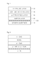
- Fig. 1 is a schematic sectional view of a nitride-based light emitting device according to an exemplary embodiment of the present invention.
- the nitride-based light emitting device includes a growth substrate 110, a seed layer 120 for nitride growth, a p-type nitride layer 130, a light emitting active layer 140, and an n-type ZnO layer 150.
- the growth substrate 110 may be a sapphire substrate which is widely used as a growth substrate in manufacture of nitride-based light emitting devices.
- the growth substrate 110 may be a silicon substrate such as a single crystal silicon substrate, a polycrystal silicon substrate, and the like.
- the seed layer 120 for nitride growth is a powder type seed layer formed on the growth substrate 110 and acts as seeds for growth of a nitride layer.
- the term "powder type" refers to a material formed of powder.
- the seed layer 120 for nitride growth relieves lattice mismatch with respect to a nitride layer to be grown, thereby decreasing dislocation density during growth of the nitride layer.
- dislocation density increases to a great extent during growth of the nitride layer on the silicon substrate due to a great difference in lattice constant between the silicon substrate and the nitride layer, thereby causing deterioration in luminous efficacy of the light emitting device.
- the seed layer for nitride growth is formed on the silicon substrate and the nitride layer is then formed on the seed layer for nitride growth, lattice mismatch between the nitride layer and the substrate is relieved, thereby reducing dislocation density caused by lattice mismatch during growth of the nitride layer
- Such a seed layer 120 for nitride growth may be comprised of GaN powder, sapphire powder or silica powder, which can relieve lattice mismatch with respect to a nitride.
- the nitride layer is initially grown in the vertical direction and then grows in the horizontal direction, thereby enabling growth of a flat nitride layer.
- the GaN, sapphire or silica powder may be attached or secured to the growth substrate 110 by spin coating, or the like.
- the growth substrate 110 may have an uneven surface formed with prominences and depressions.
- the surface unevenness may be formed as a specific or random pattern.
- the surface unevenness of the growth substrate 110 may be formed by various methods such as etching or the like.
- the GaN, sapphire or silica powder may be easily attached or secured to the depressions of the uneven surface of the growth substrate 110.
- the powder such as the GaN powder or the like applied to the seed layer for nitride growth may have an average particle size of 10 nm ⁇ 1 ⁇ m.
- the p-type nitride layer 130 is formed on the seed layer 120 for nitride growth.
- the p-type nitride layer 130 is formed by doping a p-type impurity such as magnesium (Mg) and the like to ensure p-type electrical characteristics.
- the p-type nitride layer is formed at the last stage after the light emitting active layer is formed.
- the p-type nitride layer is grown at a lower growth temperature to suppress influence of the p-type impurity on the light emitting active layer during formation of the p-type nitride layer.
- crystal quality of the p-type nitride layer is deteriorated, causing deterioration of light emitting efficiency.
- the p-type nitride layer 130 is formed before the light emitting active layer 140, thereby ensuring high crystal quality of the p-type nitride layer.
- the light emitting active layer 140 is formed on the p-type nitride layer 130.
- the light emitting active layer 140 may have a multiple quantum well (MQW) structure.
- MQW multiple quantum well
- the light emitting active layer 140 may have a structure having In x Ga 1-x N (0.1 ⁇ x ⁇ 0.3) and GaN alternately stacked one above another or a structure having ln x Zn 1-x O (0.1 ⁇ x ⁇ 0.3) and ZnO alternately stacked one above another.
- the n-type ZnO layer 150 is formed on the light emitting active layer 140 and exhibits opposite electrical characteristics to those of the p-type nitride layer 130.
- ZnO is an n-type material, ZnO has insignificant electrical characteristics compared with those of the n-type layer formed using n-type impurities and may act merely as a current path.
- n-type impurities such as silicon (Si) may be doped into the n-type ZnO layer 150.
- ZnO has a Wurtzite lattice structure that is substantially the same as that of GaN.
- ZnO can be grown even at a temperature of about 700 ⁇ 800°C, it is possible to improve crystal quality by minimizing influence on the light emitting active 140 during growth of ZnO.
- the n-type ZnO layer 150 applicable to the present invention can replace n-type GaN, which is grown at high temperature of about 1200°C.
- n-type ZnO layer 150 results in further improvement of brightness as compared with the case where the n-type GaN layer is used.
- the p-type nitride layer 130 is first formed on the growth substrate and the n-type ZnO layer 150 is then formed on the light emitting active layer.
- Fig. 2 is a schematic sectional view of a nitride-based light emitting device, which includes a p-type silicon substrate as a growth substrate, according to an exemplary embodiment of the present invention.
- the nitride-based light emitting device may employ the p-type silicon substrate as the growth substrate.
- the p-type silicon substrate When the p-type silicon substrate is adopted, p-type layers may be formed as the respective layers under the light emitting active layer. Further, when the p-type silicon substrate is adopted, the silicon substrate may act as a p-electrode, thereby eliminating a process of removing the substrate and a process of forming the p-electrode, even in manufacture of a vertical light emitting device.
- the light emitting structure may further include a buffer layer 160 between the seed layer 120 and the p-type nitride layer 130.
- the buffer layer 160 serves to relieve stress generated during growth of the nitride layer, which is a hetero-material, on the growth substrate.
- Such a buffer layer 160 may be comprised of a nitride material such as AIN, ZrN, GaN, or the like.
- the buffer layer 160 may be a p-type buffer layer. Nitrides for the buffer layer 160 generally have high electric resistance. However, if the buffer layer 160 is the p-type buffer layer, the buffer layer has low electric resistance. Accordingly, it is possible to improve operational efficiency of the nitride-based light emitting device
- the buffer layer 160 is the p-type layer and the p-type silicon substrate is used as the growth substrate 110, holes can easily move from the p-type silicon substrate to the light emitting active layer 140 without interference of a barrier, thereby further improving operational efficiency of the light emitting device.
- the buffer layer 160 is a p-type buffer layer
- impurities such as magnesium (Mg) in the buffer layer 160 diffuse into the growth substrate 110.
- the substrate exhibits electrical characteristics of a p-type layer.
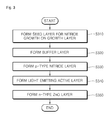
- Fig. 3 is a schematic flowchart of a method of manufacturing the nitride-based light emitting device according to an exemplary embodiment of the present invention.
- the method of manufacturing a nitride-based light emitting device includes forming a seed layer for nitride growth in operation S310, forming a buffer layer in operation S320, forming a p-type nitride layer in operation S330, forming a light emitting active layer in operation S340, and forming an n-type ZnO layer in operation S350.
- the seed layer for nitride growth is formed on a growth substrate such as a silicon substrate or a sapphire substrate
- the seed layer for nitride growth may be formed using GaN powder, sapphire powder or silica powder.
- the seed layer for nitride growth may be formed using these powders according to the following method.
- GaN powders or the like are coated on the growth substrate using a spin coater or the like. Then, the growth substrate is heated to about 800 ⁇ 1200°C in an ammonia gas atmosphere in a chamber, for example a CVD chamber, such that the GaN powders are attached to the growth substrate.
- the growth substrate may be slightly etched to form an uneven surface. The surface unevenness of the growth substrate facilitates attachment or securing of the powders thereto.
- the seed layer for nitride growth may be formed using a solution containing the GaN powders or the like by spin-coating the solution onto the growth substrate and drying the growth substrate.
- the solution containing the GaN powders may be prepared using various solvents, such as acetone, methanol, ethylene glycol, and the like.
- the seed layer for nitride growth may be formed by spin-coating and drying the solution containing the GaN powders or the like on the growth substrate, followed by heating the growth substrate in a chamber.
- a plurality of nitride layers is sequentially grown on the seed layer to form a light emitting structure through operation S320 of forming a buffer layer, operation S330 of forming a p-type nitride layer, and operation S340 of forming a light emitting active layer.
- the n-type ZnO layer is grown on the light emitting active layer in an atmosphere of nitrogen (N 2 ), helium (He), oxygen (O 2 ), or the like at a low temperature of about 700 ⁇ 800°C.
- a p-type nitride layer is formed on a growth substrate, followed by forming an n-type ZnO layer, which can be grown at relatively low temperature, on a light emitting active layer.
- a seed layer for nitride growth is formed using GaN powder, sapphire powder or silica powder, thereby minimizing dislocation density caused by a difference in lattice constant between the silicon substrate and a nitride layer during growth of the nitride layer.
- a p-type nitride layer may be formed on a growth substrate, thereby improving crystal quality of the p-type nitride layer.
- an n-type ZnO layer capable of being grown at relatively lower temperature is formed on a light emitting active layer, it is possible to reduce influence on the light emitting active layer.
- GaN powder, sapphire powder or silica powder is used to form a seed layer for nitride growth, thereby minimizing dislocation defects caused by a difference in lattice constant between the nitride layer and the silicon substrate during growth of the nitride layer.
- a p-type silicon substrate is used, thereby facilitating manufacture of a vertical type light emitting device without a process of removing a substrate.
Landscapes
- Led Devices (AREA)
- Crystals, And After-Treatments Of Crystals (AREA)
Applications Claiming Priority (1)
| Application Number | Priority Date | Filing Date | Title |
|---|---|---|---|
| KR1020110018226A KR101053115B1 (ko) | 2011-02-28 | 2011-02-28 | 결정성 및 휘도가 우수한 질화물계 발광소자 및 그 제조 방법 |
Publications (2)
| Publication Number | Publication Date |
|---|---|
| EP2492952A2 true EP2492952A2 (de) | 2012-08-29 |
| EP2492952A3 EP2492952A3 (de) | 2014-01-15 |
Family
ID=44932677
Family Applications (1)
| Application Number | Title | Priority Date | Filing Date |
|---|---|---|---|
| EP11167413.1A Withdrawn EP2492952A3 (de) | 2011-02-28 | 2011-05-25 | Lichtemittierende Vorrichtung auf Nitridbasis mit hervorragender Kristallinität und Helligkeit und Verfahren zu ihrer Herstellung |
Country Status (7)
| Country | Link |
|---|---|
| US (1) | US20120217470A1 (de) |
| EP (1) | EP2492952A3 (de) |
| JP (1) | JP2012182418A (de) |
| KR (1) | KR101053115B1 (de) |
| CN (1) | CN102651440A (de) |
| TW (1) | TW201236201A (de) |
| WO (1) | WO2012118248A1 (de) |
Families Citing this family (1)
| Publication number | Priority date | Publication date | Assignee | Title |
|---|---|---|---|---|
| US9939664B2 (en) * | 2014-12-10 | 2018-04-10 | The Boeing Company | High temperature range and high strain range transparent composites based on matrices having optically tunable refractive indices |
Family Cites Families (9)
| Publication number | Priority date | Publication date | Assignee | Title |
|---|---|---|---|---|
| JP3498140B2 (ja) | 2001-01-25 | 2004-02-16 | 独立行政法人産業技術総合研究所 | 半導体発光素子 |
| KR20050104034A (ko) * | 2004-04-27 | 2005-11-02 | 삼성에스디아이 주식회사 | 나노와이어 제조방법 |
| KR100932500B1 (ko) * | 2004-09-10 | 2009-12-17 | 갤럭시아포토닉스 주식회사 | 광 추출 효율이 향상된 질화갈륨 소자 및 그 제작방법 |
| CN101068890B (zh) * | 2004-12-01 | 2011-01-19 | 康乃尔研究基金会有限公司 | 第iii族氮化物涂层及方法 |
| JP5034035B2 (ja) | 2005-08-29 | 2012-09-26 | 国立大学法人静岡大学 | 半導体発光素子の製造方法 |
| KR101220042B1 (ko) * | 2006-02-20 | 2013-01-18 | 엘지이노텍 주식회사 | 질화물 반도체 발광소자 및 그 제조 방법 |
| KR101203140B1 (ko) * | 2006-05-12 | 2012-11-20 | 서울옵토디바이스주식회사 | 산화아연계 발광 소자의 제조 방법 및 그에 의해 제조된산화아연계 발광 소자 |
| KR100966367B1 (ko) * | 2007-06-15 | 2010-06-28 | 삼성엘이디 주식회사 | 반도체 발광소자 및 그의 제조방법 |
| KR101047761B1 (ko) * | 2008-12-26 | 2011-07-07 | 엘지이노텍 주식회사 | 반도체 발광소자 |
-
2011
- 2011-02-28 KR KR1020110018226A patent/KR101053115B1/ko not_active Expired - Fee Related
- 2011-05-25 EP EP11167413.1A patent/EP2492952A3/de not_active Withdrawn
- 2011-05-27 TW TW100118764A patent/TW201236201A/zh unknown
- 2011-05-27 CN CN2011101403330A patent/CN102651440A/zh active Pending
- 2011-06-03 WO PCT/KR2011/004058 patent/WO2012118248A1/ko not_active Ceased
- 2011-06-21 JP JP2011137869A patent/JP2012182418A/ja not_active Withdrawn
- 2011-07-24 US US13/189,519 patent/US20120217470A1/en not_active Abandoned
Non-Patent Citations (1)
| Title |
|---|
| None |
Also Published As
| Publication number | Publication date |
|---|---|
| KR101053115B1 (ko) | 2011-08-01 |
| US20120217470A1 (en) | 2012-08-30 |
| EP2492952A3 (de) | 2014-01-15 |
| TW201236201A (en) | 2012-09-01 |
| CN102651440A (zh) | 2012-08-29 |
| JP2012182418A (ja) | 2012-09-20 |
| WO2012118248A1 (ko) | 2012-09-07 |
Similar Documents
| Publication | Publication Date | Title |
|---|---|---|
| JP5130433B2 (ja) | 窒化物半導体発光素子及びその製造方法 | |
| CN106505133A (zh) | 紫外发光器件及其制造方法 | |
| KR20100093872A (ko) | 질화물 반도체 발광소자 및 그 제조방법 | |
| KR20040005630A (ko) | 화합물 반도체 발광 소자용 에피택셜 기판, 이의 제조방법및 발광 소자 | |
| US20120217537A1 (en) | Nitride based light emitting device using patterned lattice buffer layer and method of manufacturing the same | |
| CN108447952A (zh) | 一种发光二极管外延片及其制备方法 | |
| EP2492974A2 (de) | Nitridbasierte lichtemittierende Vorrichtung mit einer Pufferschicht aus Wurtzit-Pulver und Verfahren zu ihrer Herstellung | |
| US20120217504A1 (en) | Nitride based light emitting device using silicon substrate and method of manufacturing the same | |
| KR101042561B1 (ko) | 결정성 및 휘도가 우수한 질화물계 발광소자 및 그 제조 방법 | |
| EP2492972A2 (de) | Verfahren zur Herstellung von GaN-Pulver und lichtemittierende Vorrichtung auf Nitridbasis mit anhand des Verfahrens hergestelltem GaN-Pulver | |
| EP2492952A2 (de) | Lichtemittierende Vorrichtung auf Nitridbasis mit hervorragender Kristallinität und Helligkeit und Verfahren zu ihrer Herstellung | |
| TWI545798B (zh) | Nitride semiconductor light emitting device and manufacturing method thereof | |
| JP2008227103A (ja) | GaN系半導体発光素子 | |
| KR101379341B1 (ko) | 마스크 패턴을 삽입한 고품질 반도체 소자용 기판의 제조 방법 | |
| CN106848008B (zh) | 一种利用v型缺陷改善led光电特性的方法 | |
| JP6649693B2 (ja) | 窒化物半導体発光素子及びその製造方法 | |
| KR20120138049A (ko) | 발광 효율 및 전기적 특성이 우수한 질화물계 발광소자 및 그 제조 방법 | |
| KR20120138050A (ko) | 초격자 버퍼층을 이용한 질화물계 발광소자 및 그 제조 방법 | |
| KR101471425B1 (ko) | 양자섬을 삽입한 고품질 반도체 소자용 기판의 제조 방법 | |
| JP2007201152A5 (de) | ||
| KR20140099693A (ko) | 무분극 질화물계 발광 소자 및 그 제조 방법 | |
| KR20130048844A (ko) | 발광 다이오드 및 그 제조 방법 |
Legal Events
| Date | Code | Title | Description |
|---|---|---|---|
| PUAI | Public reference made under article 153(3) epc to a published international application that has entered the european phase |
Free format text: ORIGINAL CODE: 0009012 |
|
| AK | Designated contracting states |
Kind code of ref document: A2 Designated state(s): AL AT BE BG CH CY CZ DE DK EE ES FI FR GB GR HR HU IE IS IT LI LT LU LV MC MK MT NL NO PL PT RO RS SE SI SK SM TR |
|
| AX | Request for extension of the european patent |
Extension state: BA ME |
|
| PUAL | Search report despatched |
Free format text: ORIGINAL CODE: 0009013 |
|
| AK | Designated contracting states |
Kind code of ref document: A3 Designated state(s): AL AT BE BG CH CY CZ DE DK EE ES FI FR GB GR HR HU IE IS IT LI LT LU LV MC MK MT NL NO PL PT RO RS SE SI SK SM TR |
|
| AX | Request for extension of the european patent |
Extension state: BA ME |
|
| RIC1 | Information provided on ipc code assigned before grant |
Ipc: H01L 33/00 20100101ALI20131210BHEP Ipc: H01L 21/02 20060101AFI20131210BHEP Ipc: H01L 21/20 20060101ALI20131210BHEP Ipc: H01L 33/28 20100101ALI20131210BHEP |
|
| STAA | Information on the status of an ep patent application or granted ep patent |
Free format text: STATUS: THE APPLICATION IS DEEMED TO BE WITHDRAWN |
|
| 18D | Application deemed to be withdrawn |
Effective date: 20131203 |