EP2492984B1 - Spinfiltervorrichtung, Verfahren zu deren Herstellung und Verwendung - Google Patents
Spinfiltervorrichtung, Verfahren zu deren Herstellung und Verwendung Download PDFInfo
- Publication number
- EP2492984B1 EP2492984B1 EP12153747.6A EP12153747A EP2492984B1 EP 2492984 B1 EP2492984 B1 EP 2492984B1 EP 12153747 A EP12153747 A EP 12153747A EP 2492984 B1 EP2492984 B1 EP 2492984B1
- Authority
- EP
- European Patent Office
- Prior art keywords
- monolayer
- spin
- substrate
- electrons
- molecules
- Prior art date
- Legal status (The legal status is an assumption and is not a legal conclusion. Google has not performed a legal analysis and makes no representation as to the accuracy of the status listed.)
- Active
Links
Images




Classifications
-
- H—ELECTRICITY
- H10—SEMICONDUCTOR DEVICES; ELECTRIC SOLID-STATE DEVICES NOT OTHERWISE PROVIDED FOR
- H10D—INORGANIC ELECTRIC SEMICONDUCTOR DEVICES
- H10D48/00—Individual devices not covered by groups H10D1/00 - H10D44/00
- H10D48/385—Devices using spin-polarised carriers
-
- B—PERFORMING OPERATIONS; TRANSPORTING
- B82—NANOTECHNOLOGY
- B82Y—SPECIFIC USES OR APPLICATIONS OF NANOSTRUCTURES; MEASUREMENT OR ANALYSIS OF NANOSTRUCTURES; MANUFACTURE OR TREATMENT OF NANOSTRUCTURES
- B82Y10/00—Nanotechnology for information processing, storage or transmission, e.g. quantum computing or single electron logic
-
- H—ELECTRICITY
- H10—SEMICONDUCTOR DEVICES; ELECTRIC SOLID-STATE DEVICES NOT OTHERWISE PROVIDED FOR
- H10K—ORGANIC ELECTRIC SOLID-STATE DEVICES
- H10K10/00—Organic devices specially adapted for rectifying, amplifying, oscillating or switching; Organic capacitors or resistors having potential barriers
- H10K10/701—Organic molecular electronic devices
-
- H—ELECTRICITY
- H10—SEMICONDUCTOR DEVICES; ELECTRIC SOLID-STATE DEVICES NOT OTHERWISE PROVIDED FOR
- H10K—ORGANIC ELECTRIC SOLID-STATE DEVICES
- H10K85/00—Organic materials used in the body or electrodes of devices covered by this subclass
- H10K85/761—Biomolecules or bio-macromolecules, e.g. proteins, chlorophyl, lipids or enzymes
Definitions
- the present invention relates to a method and a device for providing a current of spin-polarised electrons. More particularly, the present invention is suited for use in spin electronics or detection of spin-polarised electrons.
- spintronics or spin electronics
- spin electronics refers to the role played by electron spin in solid state physics, and to devices that specifically exploit spin properties, i.e. spin degrees of freedom, instead of, or in addition to, charge degrees of freedom.
- spin relaxation and spin transport in metals and semiconductors are of interest in fundamental research such as solid state physics and more generally in other electronic technology areas. Extensive research and development is carried out in the field of spintronics with the objective to fully utilise the advantage that no electron charges need to be transported which would cost energy and produce heat.
- currents of spin-polarised electrons can be obtained when circularly polarised light ejects electrons from substrates with large spin-orbit coupling, for example gallium arsenide (GaAs).
- GaAs gallium arsenide
- Spin-polarised electrons can further be obtained by filtering photoelectrons ejected from a gold substrate via a self-assembled layer of double-stranded DNA ( S.G. Ray et al., Phys. Rev. Lett. 96, 036101, 2006 ).
- the materials used are prepared in complex preparations under ultra-high vacuum (UHV) conditions.
- UHV ultra-high vacuum
- the degree of polarisation of free spin-polarised electrons is presently measured by so called Mott scattering of high energy electrons on thin gold foil under high vacuum conditions.
- the high energy electrons are in the region of more than 50 kV and the thin gold foil is in the region of a few nanometres.
- the degree of polarisation of free spin-polarised electrons can be measured by spin-dependent diffraction at surfaces of wolfram (W) or iron (Fe) under ultra-high vacuum conditions (less than 10 10 mbar).
- W wolfram
- Fe iron
- an apparatus comprising a photon source producing incident light of linearly polarised or unpolarised photons; and a spin filter device, wherein the spin filter device comprises
- the molecules of said at least one monolayer are chiral molecules.
- Chiral molecules lack mirror image symmetry and show two types of enantiomers that can be described as left-handed (L- or levo-) and right-handed (D- or dextro-) species.
- L- or levo- left-handed
- D- or dextro- right-handed species.
- the substrate comprises a semiconductor layer.
- the substrate can optionally be polycrystalline or single crystalline.
- An example of the substrate suitable for the spin filter device of the present invention can include, but is not limited to, polycrystalline gold (Au) or single crystalline gold (Au(111)).
- the at least one monolayer is self-assembled on the substrate, produced for example in a wet chemical procedure.
- the said at least one monolayer can optionally comprise organic molecules.
- the said at least one monolayer can comprise nano-particles, particularly nano-dots.
- the molecules of the said at least one monolayer can optionally be thiolated molecules.
- An example of the thiolated molecules suitable for the spin filter device of the invention can include, but is not limited to, double stranded DNA. Double stranded DNA is chiral both because of its primary structure and because of its secondary, double helix structure.
- the molecules can have a predetermined length, e.g. the double stranded DNA can comprise for example 40, 50, 78 or any other number of base pairs (bp) as considered appropriate for particular application of the present invention.
- a method for manufacturing a spin filter device including the steps of
- the substrate and the at least one monolayer can include all or selected features of the substrate and the monolayer, respectively, and its preferred embodiments as defined in relation to the aspect of the disclosure further above in which a spin filter device is provided, as considered appropriate for manufacturing the spin filter device.
- Step (a) of the method can optionally include cleaning the substrate prior to step (b), for example by sputtering with rare or reactive gases or by wet chemical agents.
- the at least one monolayer is deposited upon the substrate by self-assembling of the molecules.
- the self-assembling of the molecules can optionally be processed in a wet chemical procedure.
- step (b) of the method can include integrating nano-particles, particularly nano-dots, into the at least one monolayer.
- the nano-particles can optionally be integrated between the monolayers.
- a method for using a spin filter device for generating a current having a first substrate and at least one monolayer deposited on the first substrate including the steps of
- the at least one monolayer can include all or selected features of the monolayer and its preferred embodiments as defined in relation to the aspect of the disclosure in which a spin filter device is provided, as considered appropriate for using the spin filter device.
- step (a) of the method can include irradiating said substrate with photons from a photon source thereby producing a current of photoelectrons which travel into said at least one monolayer.
- step (a) of the method can include irradiating said substrate with a UV laser pulse.
- a photon energy of the photoelectrons emitted by the UV laser can be 5.84 eV, wherein the pulse duration can be about 200 ps (picoseconds) at 20 kHz repetition rate, and a fluence of 150 pJ/cm 2 .
- the laser pulse can optionally be generated from a ND:YVO oscillator.
- step (a) can be realised by electric or magnetic field induced injection from a spin polarised substrate.
- Step (a) can optionally include irradiating said substrate with linearly or circularly polarised photons.
- a spintronic transistor structure including a semiconductor structure carrying a spin filter device including all or selected features of the spin filter device and its preferred embodiments as defined in relation to the aspect of the disclosure in which a spin filter device is provided, wherein the spin filter device is adapted to operate as a spin injector for the semiconductor structure.
- the semiconductor structure can comprise silicon or GaAs.
- a detector for spin-polarised electrons including at least one monolayer
- the molecules of the at least one monolayer are chiral molecules.
- the said at least one monolayer can optionally comprise organic molecules.
- the at least one monolayer is self-assembled on the detector, for example in a wet chemical procedure.
- the at least one monolayer can optionally comprise nano-particles, particularly nano-dots.
- An advantage of embodiments of the present invention is that magnetic or magnetized substrates are no longer needed to generate spin-polarised electrons. Also, circularly polarised light is no longer needed to generate spin-polarised electrons.
- the materials can be easily prepared, for example by wet chemical procedures, and have turned out to be stable in air. So, they can be used in room temperature and do not need expensive cooling.
- a further advantage of the present invention is that it provides an effective way to inject spin into standard transistors, such as silicon based transistor.
- the invention further enables spin sensitive gating. Furthermore the invention enables the reduction of the amount of space and heat capacitance of logic devices.
- Fig. 1 shows a perspective view of a spin filter device 10 according to one embodiment of the disclosure.
- the spin filter device 10 includes a monolayer 12 of double stranded DNA (dsDNA).
- Thiolated dsDNA is bound to a substrate 14, which is a gold surface in this example, and forms a self-assembled monolayer 12 of chiral molecules.
- the substrate can also be formed by any other material, e.g. a different metal or a semiconductor.
- Unpolarised electrons 16 ejected from the gold surface produced by linearly polarised light 18 incident from the monolayer side are transmitted and can be analyzed. Most of the electrons 20 transmitted through the monolayer 12 are polarised with their spin aligned anti-parallel to their velocity.
- spin-polarised photoelectrons are readily generated from magnetic substrates or when circularly polarised light ejects electrons from substrates with large spin-orbit coupling. Since an organic chiral layer on a non-magnetic metal surface is not likely to be self-magnetized, one expects that photoelectrons ejected from such a layer with unpolarised light will not be spin polarised.
- the present invention shows exceptionally high polarisation of electrons which are ejected from surfaces coated with self-assembled monolayer of double stranded DNA, independent of the polarisation of the incident light.
- self-assembled dsDNA monolayers can be prepared according to standard procedures by depositing dsDNA which is thiolated on one, e.g. the 3', end of one of the DNA strands on a clean gold substrate.
- Either polycrystalline Au or single crystal Au(111) may be used as substrates.
- the monolayers are characterized by various methods that ensure the uniformity and reproducibility of the DNA layer. The experiments have been carried out under ultra-high vacuum conditions that employed photoelectron detection with two detectors, an electron time-of-flight instrument, recording the kinetic energy distribution of the electrons, and a Mott-type electron polarimeter for spin analysis.
- the photoelectrons were ejected by a UV laser pulse with a photon energy of 5.84 eV, pulse duration of about 200 ps at 20 kHz repetition rate, and a fluence of 150 pJ/cm 2 .
- the laser light is normally incident onto the sample, and it is either linearly or circularly polarised. For the vast majority of DNA samples no damage is observed over the course of the spin polarisation measurement within about four hours.
- the photoelectrons are guided by an electrostatic 90°-bender and subsequent transport optics. Hence, an initial longitudinal spin polarisation is converted into a transversal one for analysis.
- I U,L denote the count rates of an upper and a lower counter.
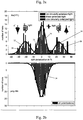
- Fig. 2a and Fig. 2b illustrate examples of measurements of spinpolarisation with prior art devices.
- the spin polarisation of photoelectrons from a clean Au(111) single crystal is shown for different laser polarisations.
- the spin polarisation and the sign of its orientation depend on the laser polarisation.
- Fig. 4 shows measurements of the electron spin polarisation for various monolayers 12 ( Fig. 1 ) of DNA on polycrystalline gold (Au) surfaces. More specifically, room temperature electron spin polarisations are presented for four different monolayers of dsDNA in which each of the molecules have different lengths of 28, 40, 50, and 78 base pairs (line with filled dots shown at 42a,b,c, 44a,b,c, 46a,b,c, 48a,b,c). The results of 36 different experiments on ten different samples are shown. Further, monolayers of single stranded DNA (lines with open diamond shown at 50a,b,c), and a sample of dsDNA damaged by UV light (lines with open triangle shown at 52a,b,c) are investigated.
- the molecules are more floppy and do not form rigid close-packed monolayers and indeed no spin selectivity is observed. Because the photon energy is lower than the ionization energy of the DNA and the laser intensity is low, the photoelectrons all originate from the gold substrate. In addition, less than 0.1% of the incident light is absorbed in the layer, even under resonance conditions. The low intensities and weak absorbances ensure further that non-linear excitation processes do not occur in the DNA layer.
- Electrons are known to transmit through free standing or supported thin ferromagnetic films that acted as a spin filter in certain situations. In these cases, and for low-energy electrons, the selectivity was reported to be about 25%.
- the spin polarisation can be explained by inelastic electron scattering involving unoccupied d-states above the Fermi level. The scattering rate for minority spin electrons is then enhanced with respect to that of majority spin electrons because of an excess of minority spin holes.
- the polarisation decreased sharply as a function of collision energies, due to the spin dilution by secondary electrons.
- the polarisation is energy independent within the energy range studied. Although polarised light is not needed, the polarisation achieved with embodiments of the present invention is almost as high as that obtained by photoemission with circular polarised light from GaAs substrates.
- Fig. 5 shows the kinetic energy distribution of the electrons 16, 20 ( Fig. 1 ) transmitted through the self-assembled monolayer 12 ( Fig. 1 ) of dsDNA (50 bp) adsorbed on a polycrystalline Au substrate 14 ( Fig. 1 ) for clockwise (cw, curve 56) and counter clockwise (ccw, curve 58) circularly polarised light.
- Photoelectrons with kinetic energies up to about 1.2 eV are measured.
- the intensity of the signal (curve 58) observed with ccw polarised radiation is larger by about 7% relative to that obtained with the cw light (curve 56). This ratio is independent of the primary kinetic energy of the photo-emitted electrons.
- This result clearly shows a circular dichroism which is consistent with the results obtained in Fig. 2a . In this measurement the electron signal is not spin resolved. It further shows that the work function is independent of the handedness of the light, as expected.
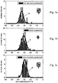
- Fig. 6a, 6b, 6c , 7a, 7b, 7c , 8a, 8b and 8c typical results for one preparation are shown for 40 bp, 50 bp, and 78 bp monolayers 12 ( Fig. 1 ) of dsDNA on poly-Au substrates 14 ( Fig. 1 ).
- Fig. 6a, 6b and 6c show measurements of the spin polarisation of 40bp dsDNA/poly-Au.
- the spin polarisation is (38.0 ⁇ 6.5) % for linear polarised light ( Fig. 6a ), (35.1 ⁇ 8.3) % for cw polarised light ( Fig. 6b ), and (40.1 ⁇ 5.5) % for ccw polarised light ( Fig. 6c ).
- Fig. 7a, 7b and 7c show measurements of the spin polarisation of 50bp dsDNA/poly-Au.
- the spin polarisation is (35.5 ⁇ 5.5) % for linear polarised light ( Fig. 7a ), (31.5 ⁇ 5.7) % for cw polarised light ( Fig. 7b ), and (38.8 ⁇ 5.9) % for ccw polarised light ( Fig. 7c ).
- Fig. 8a, 8b and 8c show measurements of the spin polarisation of 78bp dsDNA/poly-Au.
- the spin polarisation is -(57.2 ⁇ 5.9) % for linear polarised light ( Fig. 8a ), -(54.5 ⁇ 7.0) % for cw polarised light ( Fig. 8b ), and -(60.8 ⁇ 5.8) % for ccw polarised light ( Fig. 8c ).
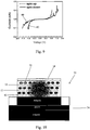
- Fig. 9 shows the spin dependent current through double stranded DNA which is 40 base pairs long.
- the current of electrons with spin up is shown in curve 60, whereas the current of electrons with spin down is shown in curve 62.
- the ratio between the two spin currents 60, 62 is 1:5.
- Fig. 10 shows a spintronic transistor structure 70 according to an embodiment of the disclosure. It comprises three monolayers 12 of organic molecules and nano-dots 72 incorporated between the monolayers 12. The monolayers 12 are self-assembled to the substrate 14 which is made of gold (Au).
- the spintronic transistor structure 70 is based on a semiconductor structure 74 comprising GaAs.
- the transistor 70 can create discrete gating for non binary logic operation. By creating several plateaus-like features in the IV characteristics of the transistors 70 a reduction of the power of standard transistors working in non binary base may be obtained.
- a spin filter device 80 is shown as an example for a further embodiment according to the present disclosure.
- a first substrate 82 e.g. a metal or a semiconductor, acts as source material.
- a monolayer 86 of asymmetrical molecules, preferably organized chiral molecules is deposited upon the first substrate 82.
- the first substrate 82 and the monolayer 86 form the spin filter device.
- a second substrate 84 which can be for example a metal, a semiconductor, an isolator or a vacuum, acts as target material.
- the monolayer 86 is located between the first and the second substrate 82, 84.
- the monolayer 86 is deposited upon or bounded to the first substrate 82 by self-assembling. Electrons (not shown) travel from the first substrate 84 into the monolayer 86. The majority of those electrons which have passed the monolayer 86 have the same spin. These spin filtered or spin-polarised electrons are injected into the second substrate 84.
- the present invention provides for practical and theoretical considerations allowing for configuring a novel spin filter device that can be used in spintronic devices.
- This structure is characterized by spin selectivity for electron transmission therethrough.
- the spin filter device of the present disclosure can be used in a spintronic transistor structure.
- the structure can also be used as components in other detectors or sensors.
Landscapes
- Engineering & Computer Science (AREA)
- Chemical & Material Sciences (AREA)
- Physics & Mathematics (AREA)
- Nanotechnology (AREA)
- Spectroscopy & Molecular Physics (AREA)
- Crystallography & Structural Chemistry (AREA)
- Theoretical Computer Science (AREA)
- Mathematical Physics (AREA)
- Materials Engineering (AREA)
- Molecular Biology (AREA)
- General Health & Medical Sciences (AREA)
- Biophysics (AREA)
- Biochemistry (AREA)
- Life Sciences & Earth Sciences (AREA)
- Health & Medical Sciences (AREA)
- Apparatus Associated With Microorganisms And Enzymes (AREA)
- Investigating, Analyzing Materials By Fluorescence Or Luminescence (AREA)
- Compositions Of Oxide Ceramics (AREA)
- Networks Using Active Elements (AREA)
- Radiation Pyrometers (AREA)
Claims (10)
- Vorrichtung, enthaltend:eine Photonenquelle, die einfallendes Licht linear polarisierter oderunpolarisierter Photonen erzeugt; undein Spinfiltergerät (10, 80),wobei das Spinfiltergerät (10, 80) enthält:ein Substrat (14, 82), wobei das Substrat eine Halbleiterschicht enthält, undzumindest eine Monolage (12, 86), wobei die zumindest eine Monolage (12, 86) selbstorganisiert auf besagtem Substrat (14, 82), das dem besagten einfallenden Licht ausgesetzt werden soll, ist, wobei eine Bestrahlung der zumindest einen Monolage mit dem einfallenden Licht ein Herauslösen von Photoelektronen aus besagter Halbleiterschicht bewirkt,wobei die Monolage (12, 86) asymmetrische Moleküle enthält, und geeignet ist, Elektronen (16), die vom Substrat (14, 82) durch die zumindest eine Monolage (12, 86) wandern, derart zu filtern, dass Elektronen (20), die eine vorbestimmte Spinpolarisation aufweisen, passieren können, um einen Strom von spinpolarisierten Elektronen (20) zu erzeugen, wobei besagte Spinpolarisation von der Polarisation des einfallenden Lichts unabhängig ist,wobei die Moleküle der zumindest einen Monolage chirale Moleküle sind.
- Vorrichtung nach Anspruch 1, dadurch gekennzeichnet, dass das Substrat (14, 82) polykristallin oder einkristallin ist.
- Vorrichtung nach einem der vorangehenden Ansprüche, dadurch gekennzeichnet, dass die zumindest eine Monolage (12, 86) organische Moleküle, vorzugsweise thiolierte Moleküle und besonders bevorzugt doppelsträngige DNA, oder Nanopartikel, vorzugsweise Nanodots, enthält.
- Verfahren zur Herstellung eines Spinfiltergeräts (10, 80), umfassend die Schritte(a) Bereitstellen eines Substrats (14, 82), wobei das Substrat eine Halbleiterschicht enthält; und(b) Abscheiden zumindest einer Monolage (12, 86) auf dem Substrat, das linear polarisiertem oder unpolarisiertem einfallenden Licht ausgesetzt werden soll, Bestrahlung der zumindest einen Monolage durch das einfallende Licht, was ein Herauslösen von Photoelektronen aus der Halbleiterschicht bewirkt;wobei die zumindest eine Monolage (12, 86) asymmetrische Moleküle enthält, die geeignet sind, einen Strom von Elektronen (16) derart zu filtern, dass Elektronen (20), die eine vorbestimmte Spinpolarisation aufweisen, passieren können, um einen Strom von spinpolarisierten Elektronen (20) zu erzeugen, wobei besagte Spinpolarisation von der Polarisation des einfallenden Lichts unabhängig ist,
wobei die Moleküle der zumindest einen Monolage (12, 86) chirale Moleküle sind. - Verfahren nach Anspruch 4, dadurch gekennzeichnet, dass Schritt (a) des Verfahrens ein Reinigen des Substrats (14, 82) vor Schritt (b) umfasst, vorzugsweise durch Sputtern mit Edel- oder Reaktivgasen oder durch nasschemische Mittel.
- Verfahren nach einem der Ansprüche 4 oder 5, dadurch gekennzeichnet, dass Schritt (b) des Verfahrens ein Integrieren von Nanopartikeln, insbesondere Nanodots, in die zumindest eine Monolage umfasst, oder, falls mehr als eine Monolage vorhanden ist, die Nanopartikel zwischen den Monolagen integriert werden.
- Verwendung eines Spinfiltergeräts (10, 80) zum Erzeugen eines Stroms, das ein erstes Substrat (14, 82) und zumindest eine auf dem ersten Substrat (14, 82) abgeschiedene Monolage (12, 86) aufweist, mit den folgenden Schritten:(a) Erzeugen eines Stroms von Elektronen (16) von dem ersten Substrat (14, 82), um in die zumindest eine Monolage (12, 86) zu wandern, wobei das erste Substrat eine Halbleiterschicht enthält und linear polarisiertem oder unpolarisiertem einfallenden Licht ausgesetzt wird, wobei Bestrahlung der zumindest einen Monolage durch das einfallende Licht ein Herauslösen von Photoelektronen aus besagter Halbleiterschicht bewirkt; und(b) Injizieren von Elektronen (20), welche die zumindest eine Monolage (12, 86) passiert haben, in Vakuum;wobei die zumindest eine Monolage (12, 86) asymmetrische Moleküle enthält, die geeignet sind, den Strom von Elektronen (16) derart zu filtern, dass Elektronen (20), die eine vorbestimmte Spinpolarisation aufweisen, passieren können, um einen Strom von spinpolarisierten Elektronen (20) zu erzeugen, wobei die Spinpolarisation von der Polarisation des einfallenden Lichts unabhängig ist,
wobei die Moleküle der zumindest einen Monolage (12, 86) chirale Moleküle sind. - Verwendung nach Anspruch 7, dadurch gekennzeichnet, dass die zumindest eine Monolage (12, 86) selbstorganisiert auf dem Substrat (14, 82) ist.
- Verwendung nach einem der Ansprüche 7 oder 8, dadurch gekennzeichnet, dass die zumindest eine Monolage (12, 86) organische Moleküle, vorzugsweise thiolierte Moleküle und besonders bevorzugt doppelsträngige DANN, oder Nanopartikel, enthält.
- Verwendung nach einem der Ansprüche 7 bis 9, dadurch gekennzeichnet, dass Schritt (a) eine Bestrahlung des Substrats (14, 82) mit Photonen (18) aus einer Photonenquelle umfasst, wodurch ein Strom von Photoelektronen (16) erzeugt wird, die in die zumindest eine Monolage (12, 86) wandern, vorzugsweise mit einem UV-Laserpuls, besonders bevorzugt einem UV-Laserpuls, der von einem Nd:YVO4-Oszillator erzeugt wird, und/oder Schritt (a) eine Bestrahlung des Substrats (14, 82) mit linear oder zirkular polarisierten oder unpolarisierten Photonen umfasst.
Applications Claiming Priority (1)
| Application Number | Priority Date | Filing Date | Title |
|---|---|---|---|
| GBGB1101862.9A GB201101862D0 (en) | 2011-02-03 | 2011-02-03 | Method and device |
Publications (3)
| Publication Number | Publication Date |
|---|---|
| EP2492984A2 EP2492984A2 (de) | 2012-08-29 |
| EP2492984A3 EP2492984A3 (de) | 2014-08-06 |
| EP2492984B1 true EP2492984B1 (de) | 2019-05-01 |
Family
ID=43836145
Family Applications (1)
| Application Number | Title | Priority Date | Filing Date |
|---|---|---|---|
| EP12153747.6A Active EP2492984B1 (de) | 2011-02-03 | 2012-02-03 | Spinfiltervorrichtung, Verfahren zu deren Herstellung und Verwendung |
Country Status (3)
| Country | Link |
|---|---|
| US (2) | US9391285B2 (de) |
| EP (1) | EP2492984B1 (de) |
| GB (1) | GB201101862D0 (de) |
Cited By (1)
| Publication number | Priority date | Publication date | Assignee | Title |
|---|---|---|---|---|
| US12046269B2 (en) | 2019-10-23 | 2024-07-23 | Merck Patent Gmbh | Two bit memory device and method for operating the two-bit memory device and electronic component |
Families Citing this family (9)
| Publication number | Priority date | Publication date | Assignee | Title |
|---|---|---|---|---|
| GB201101862D0 (en) | 2011-02-03 | 2011-03-23 | Univ Muenster Wilhelms | Method and device |
| SE536362C2 (sv) * | 2011-04-15 | 2013-09-10 | Oscar Tjernberg | Spinnfilter och detektor innefattande sådan |
| US9355698B2 (en) | 2012-03-13 | 2016-05-31 | Yeda Research And Development Co. Ltd. | Memory and logic device and methods for performing thereof |
| US9548382B2 (en) * | 2012-10-12 | 2017-01-17 | Northeastern University | Spintronic device |
| CN104345331B (zh) * | 2013-07-24 | 2017-04-19 | 中国科学院上海微系统与信息技术研究所 | 图像型电子自旋分析器 |
| US20170294572A1 (en) | 2014-03-26 | 2017-10-12 | Yeda Research And Development Co. Ltd. | Spin transport electronic device |
| KR101590699B1 (ko) * | 2014-03-31 | 2016-02-02 | 경희대학교 산학협력단 | 스핀 편향 전자총과 이를 이용한 의료장치 및 전자현미경 |
| US20230301200A1 (en) * | 2020-03-08 | 2023-09-21 | Ramot At Tel-Aviv University Ltd. | Method and system for spin-dependent conduction |
| CN119486445A (zh) * | 2024-11-08 | 2025-02-18 | 北京工业大学 | 一种手性自旋极化圆偏振光电器件、制备与应用 |
Family Cites Families (14)
| Publication number | Priority date | Publication date | Assignee | Title |
|---|---|---|---|---|
| US5472881A (en) * | 1992-11-12 | 1995-12-05 | University Of Utah Research Foundation | Thiol labeling of DNA for attachment to gold surfaces |
| GB9403234D0 (en) | 1994-02-19 | 1994-04-13 | Rolls Royce Plc | A solid oxide fuel cell stack and a reactant distribution member therefor |
| JP2002265598A (ja) * | 2001-03-08 | 2002-09-18 | Katsuhiko Naoi | 無機/有機複合化系ナノビーズおよびその製造方法 |
| JP2003043037A (ja) * | 2001-07-27 | 2003-02-13 | Inst Of Physical & Chemical Res | ハイブリダイゼーション用基板、この基板の製造方法及び使用方法 |
| JP3972240B2 (ja) | 2002-06-11 | 2007-09-05 | 日産自動車株式会社 | 固体電解質型燃料電池 |
| JP4073323B2 (ja) * | 2003-01-23 | 2008-04-09 | 日立ソフトウエアエンジニアリング株式会社 | 機能性ビーズ、その読み取り方法および読み取り装置 |
| DE602004018470D1 (de) * | 2003-02-25 | 2009-01-29 | Yeda Res & Dev | Nanoskopische struktur und diese verwendende vorrichtung |
| US7906345B2 (en) * | 2003-11-12 | 2011-03-15 | The Board Of Trustees Of The Leland Stanford Junior University | Magnetic nanoparticles, magnetic detector arrays, and methods for their use in detecting biological molecules |
| TWI273733B (en) | 2005-11-08 | 2007-02-11 | Iner Ae | Solid oxide fuel cell stack of modularized design |
| JP4254823B2 (ja) | 2006-08-30 | 2009-04-15 | カシオ計算機株式会社 | 反応装置及び電子機器 |
| US20080161202A1 (en) * | 2006-12-29 | 2008-07-03 | Edelmira Cabezas | Novel strategy for selective regulation of background surface property in microarray fabrication and method to eliminated self quenching in micro arrays |
| JP2009064826A (ja) * | 2007-09-04 | 2009-03-26 | Tdk Corp | スピントランジスタ及びその製造方法 |
| JP2009087550A (ja) | 2007-09-27 | 2009-04-23 | Ngk Spark Plug Co Ltd | 固体酸化物形燃料電池 |
| GB201101862D0 (en) | 2011-02-03 | 2011-03-23 | Univ Muenster Wilhelms | Method and device |
-
2011
- 2011-02-03 GB GBGB1101862.9A patent/GB201101862D0/en not_active Ceased
-
2012
- 2012-02-03 EP EP12153747.6A patent/EP2492984B1/de active Active
- 2012-02-03 US US13/365,706 patent/US9391285B2/en not_active Expired - Fee Related
-
2016
- 2016-06-10 US US15/178,951 patent/US9966458B2/en not_active Expired - Fee Related
Non-Patent Citations (1)
| Title |
|---|
| POJEN CHUANG ET AL: "All-electric all-semiconductor spin field-effect transistors", NATURE NANOTECHNOLOGY, vol. 10, no. 1, 22 December 2014 (2014-12-22), GB, pages 35 - 39, XP055271324, ISSN: 1748-3387, DOI: 10.1038/nnano.2014.296 * |
Cited By (1)
| Publication number | Priority date | Publication date | Assignee | Title |
|---|---|---|---|---|
| US12046269B2 (en) | 2019-10-23 | 2024-07-23 | Merck Patent Gmbh | Two bit memory device and method for operating the two-bit memory device and electronic component |
Also Published As
| Publication number | Publication date |
|---|---|
| US9966458B2 (en) | 2018-05-08 |
| GB201101862D0 (en) | 2011-03-23 |
| US20120223294A1 (en) | 2012-09-06 |
| US9391285B2 (en) | 2016-07-12 |
| US20160293741A1 (en) | 2016-10-06 |
| EP2492984A3 (de) | 2014-08-06 |
| EP2492984A2 (de) | 2012-08-29 |
Similar Documents
| Publication | Publication Date | Title |
|---|---|---|
| US9966458B2 (en) | Spin filter device, method for its manufacture and its use | |
| US20160052789A1 (en) | Techniques for fabricating diamond nanostructures | |
| Farle et al. | Spin dynamics in the time and frequency domain | |
| US10983184B2 (en) | Specialized diamond materials for NMR applications | |
| Janβen et al. | Ultrafast spin dynamics in colloidal ZnO quantum dots | |
| Liu | Time-and angle-resolved photoemission spectroscopy (TR-ARPES) of TMDC monolayers and bilayers | |
| Duspayev et al. | Electric field analysis in a cold-ion source using Stark spectroscopy of Rydberg atoms | |
| US20140151771A1 (en) | Thin film deposition and logic device | |
| Awschalom | Manipulating and storing spin coherence in semiconductors | |
| Heckschen et al. | Spatio-Temporal Electron Propagation Dynamics in Au/Fe/Mg O (001) in Nonequilibrium: Revealing Single Scattering Events and the Ballistic Limit | |
| Liu et al. | Direct observation of nanofabrication influence on the optical properties of single self-assembled InAs/GaAs quantum dots | |
| Klotz et al. | Coplanar stripline antenna design for optically detected magnetic resonance on semiconductor quantum dots | |
| Hüfner | Introduction and basic principles | |
| KR20220129590A (ko) | 특히 이미징 용도의 다이아몬드 스캐닝 요소 및 그 제작방법 | |
| Rosenfeldt et al. | Time-resolved photoelectron spectroscopy of low-energy excitations of 4× 4 C60/Cu (111) | |
| Ludwig et al. | Quantum Dot Spintronics: Fundamentals and Applications | |
| Schönke | Static and Dynamic Magnetic Imaging of Diffent Magnetic Materials Using Scanning Electron Microscopy with Polarization Analysis | |
| Ciubotaru | Spin-wave excitation by nano-sized antennas | |
| Bland et al. | Optical studies of electron spin transmission | |
| Samarin et al. | Spin-dependent plasmons excitation in Fe layer on W (110) and their decay via electron emission | |
| Wahada | Ultrafast spin transport through oxide and nitride barriers measured by inverse Spin Hall effect | |
| Palmer et al. | Towards creation of iron nanodots using metastable atom lithography | |
| Nessi | Group-IV tellurides as a playground for enhanced performances in spin and angle-resolved photoemission spectroscopy | |
| Mayr | X-ray Imaging of Spin-Wave Dynamics: From Ferromagnetic to Antiferromagnetic Systems | |
| Wei | Spin-transfer-torque effect in ferromagnets and antiferromagnets |
Legal Events
| Date | Code | Title | Description |
|---|---|---|---|
| PUAI | Public reference made under article 153(3) epc to a published international application that has entered the european phase |
Free format text: ORIGINAL CODE: 0009012 |
|
| AK | Designated contracting states |
Kind code of ref document: A2 Designated state(s): AL AT BE BG CH CY CZ DE DK EE ES FI FR GB GR HR HU IE IS IT LI LT LU LV MC MK MT NL NO PL PT RO RS SE SI SK SM TR |
|
| AX | Request for extension of the european patent |
Extension state: BA ME |
|
| PUAL | Search report despatched |
Free format text: ORIGINAL CODE: 0009013 |
|
| AK | Designated contracting states |
Kind code of ref document: A3 Designated state(s): AL AT BE BG CH CY CZ DE DK EE ES FI FR GB GR HR HU IE IS IT LI LT LU LV MC MK MT NL NO PL PT RO RS SE SI SK SM TR |
|
| AX | Request for extension of the european patent |
Extension state: BA ME |
|
| RIC1 | Information provided on ipc code assigned before grant |
Ipc: H01L 51/05 20060101ALI20140701BHEP Ipc: H01L 51/00 20060101AFI20140701BHEP Ipc: H01L 29/66 20060101ALI20140701BHEP |
|
| 17P | Request for examination filed |
Effective date: 20150128 |
|
| RBV | Designated contracting states (corrected) |
Designated state(s): AL AT BE BG CH CY CZ DE DK EE ES FI FR GB GR HR HU IE IS IT LI LT LU LV MC MK MT NL NO PL PT RO RS SE SI SK SM TR |
|
| 17Q | First examination report despatched |
Effective date: 20160517 |
|
| STAA | Information on the status of an ep patent application or granted ep patent |
Free format text: STATUS: EXAMINATION IS IN PROGRESS |
|
| GRAP | Despatch of communication of intention to grant a patent |
Free format text: ORIGINAL CODE: EPIDOSNIGR1 |
|
| STAA | Information on the status of an ep patent application or granted ep patent |
Free format text: STATUS: GRANT OF PATENT IS INTENDED |
|
| INTG | Intention to grant announced |
Effective date: 20181128 |
|
| GRAS | Grant fee paid |
Free format text: ORIGINAL CODE: EPIDOSNIGR3 |
|
| GRAA | (expected) grant |
Free format text: ORIGINAL CODE: 0009210 |
|
| STAA | Information on the status of an ep patent application or granted ep patent |
Free format text: STATUS: THE PATENT HAS BEEN GRANTED |
|
| AK | Designated contracting states |
Kind code of ref document: B1 Designated state(s): AL AT BE BG CH CY CZ DE DK EE ES FI FR GB GR HR HU IE IS IT LI LT LU LV MC MK MT NL NO PL PT RO RS SE SI SK SM TR |
|
| REG | Reference to a national code |
Ref country code: GB Ref legal event code: FG4D |
|
| REG | Reference to a national code |
Ref country code: CH Ref legal event code: EP Ref country code: AT Ref legal event code: REF Ref document number: 1128107 Country of ref document: AT Kind code of ref document: T Effective date: 20190515 |
|
| REG | Reference to a national code |
Ref country code: DE Ref legal event code: R096 Ref document number: 602012059497 Country of ref document: DE |
|
| REG | Reference to a national code |
Ref country code: IE Ref legal event code: FG4D |
|
| REG | Reference to a national code |
Ref country code: NL Ref legal event code: MP Effective date: 20190501 |
|
| REG | Reference to a national code |
Ref country code: LT Ref legal event code: MG4D |
|
| PG25 | Lapsed in a contracting state [announced via postgrant information from national office to epo] |
Ref country code: NO Free format text: LAPSE BECAUSE OF FAILURE TO SUBMIT A TRANSLATION OF THE DESCRIPTION OR TO PAY THE FEE WITHIN THE PRESCRIBED TIME-LIMIT Effective date: 20190801 Ref country code: AL Free format text: LAPSE BECAUSE OF FAILURE TO SUBMIT A TRANSLATION OF THE DESCRIPTION OR TO PAY THE FEE WITHIN THE PRESCRIBED TIME-LIMIT Effective date: 20190501 Ref country code: FI Free format text: LAPSE BECAUSE OF FAILURE TO SUBMIT A TRANSLATION OF THE DESCRIPTION OR TO PAY THE FEE WITHIN THE PRESCRIBED TIME-LIMIT Effective date: 20190501 Ref country code: NL Free format text: LAPSE BECAUSE OF FAILURE TO SUBMIT A TRANSLATION OF THE DESCRIPTION OR TO PAY THE FEE WITHIN THE PRESCRIBED TIME-LIMIT Effective date: 20190501 Ref country code: HR Free format text: LAPSE BECAUSE OF FAILURE TO SUBMIT A TRANSLATION OF THE DESCRIPTION OR TO PAY THE FEE WITHIN THE PRESCRIBED TIME-LIMIT Effective date: 20190501 Ref country code: PT Free format text: LAPSE BECAUSE OF FAILURE TO SUBMIT A TRANSLATION OF THE DESCRIPTION OR TO PAY THE FEE WITHIN THE PRESCRIBED TIME-LIMIT Effective date: 20190901 Ref country code: SE Free format text: LAPSE BECAUSE OF FAILURE TO SUBMIT A TRANSLATION OF THE DESCRIPTION OR TO PAY THE FEE WITHIN THE PRESCRIBED TIME-LIMIT Effective date: 20190501 Ref country code: LT Free format text: LAPSE BECAUSE OF FAILURE TO SUBMIT A TRANSLATION OF THE DESCRIPTION OR TO PAY THE FEE WITHIN THE PRESCRIBED TIME-LIMIT Effective date: 20190501 Ref country code: ES Free format text: LAPSE BECAUSE OF FAILURE TO SUBMIT A TRANSLATION OF THE DESCRIPTION OR TO PAY THE FEE WITHIN THE PRESCRIBED TIME-LIMIT Effective date: 20190501 |
|
| PG25 | Lapsed in a contracting state [announced via postgrant information from national office to epo] |
Ref country code: GR Free format text: LAPSE BECAUSE OF FAILURE TO SUBMIT A TRANSLATION OF THE DESCRIPTION OR TO PAY THE FEE WITHIN THE PRESCRIBED TIME-LIMIT Effective date: 20190802 Ref country code: BG Free format text: LAPSE BECAUSE OF FAILURE TO SUBMIT A TRANSLATION OF THE DESCRIPTION OR TO PAY THE FEE WITHIN THE PRESCRIBED TIME-LIMIT Effective date: 20190801 Ref country code: RS Free format text: LAPSE BECAUSE OF FAILURE TO SUBMIT A TRANSLATION OF THE DESCRIPTION OR TO PAY THE FEE WITHIN THE PRESCRIBED TIME-LIMIT Effective date: 20190501 Ref country code: LV Free format text: LAPSE BECAUSE OF FAILURE TO SUBMIT A TRANSLATION OF THE DESCRIPTION OR TO PAY THE FEE WITHIN THE PRESCRIBED TIME-LIMIT Effective date: 20190501 |
|
| REG | Reference to a national code |
Ref country code: AT Ref legal event code: MK05 Ref document number: 1128107 Country of ref document: AT Kind code of ref document: T Effective date: 20190501 |
|
| PG25 | Lapsed in a contracting state [announced via postgrant information from national office to epo] |
Ref country code: IS Free format text: LAPSE BECAUSE OF FAILURE TO SUBMIT A TRANSLATION OF THE DESCRIPTION OR TO PAY THE FEE WITHIN THE PRESCRIBED TIME-LIMIT Effective date: 20190901 |
|
| PG25 | Lapsed in a contracting state [announced via postgrant information from national office to epo] |
Ref country code: CZ Free format text: LAPSE BECAUSE OF FAILURE TO SUBMIT A TRANSLATION OF THE DESCRIPTION OR TO PAY THE FEE WITHIN THE PRESCRIBED TIME-LIMIT Effective date: 20190501 Ref country code: RO Free format text: LAPSE BECAUSE OF FAILURE TO SUBMIT A TRANSLATION OF THE DESCRIPTION OR TO PAY THE FEE WITHIN THE PRESCRIBED TIME-LIMIT Effective date: 20190501 Ref country code: EE Free format text: LAPSE BECAUSE OF FAILURE TO SUBMIT A TRANSLATION OF THE DESCRIPTION OR TO PAY THE FEE WITHIN THE PRESCRIBED TIME-LIMIT Effective date: 20190501 Ref country code: AT Free format text: LAPSE BECAUSE OF FAILURE TO SUBMIT A TRANSLATION OF THE DESCRIPTION OR TO PAY THE FEE WITHIN THE PRESCRIBED TIME-LIMIT Effective date: 20190501 Ref country code: DK Free format text: LAPSE BECAUSE OF FAILURE TO SUBMIT A TRANSLATION OF THE DESCRIPTION OR TO PAY THE FEE WITHIN THE PRESCRIBED TIME-LIMIT Effective date: 20190501 Ref country code: SK Free format text: LAPSE BECAUSE OF FAILURE TO SUBMIT A TRANSLATION OF THE DESCRIPTION OR TO PAY THE FEE WITHIN THE PRESCRIBED TIME-LIMIT Effective date: 20190501 |
|
| REG | Reference to a national code |
Ref country code: DE Ref legal event code: R097 Ref document number: 602012059497 Country of ref document: DE |
|
| PG25 | Lapsed in a contracting state [announced via postgrant information from national office to epo] |
Ref country code: SM Free format text: LAPSE BECAUSE OF FAILURE TO SUBMIT A TRANSLATION OF THE DESCRIPTION OR TO PAY THE FEE WITHIN THE PRESCRIBED TIME-LIMIT Effective date: 20190501 Ref country code: IT Free format text: LAPSE BECAUSE OF FAILURE TO SUBMIT A TRANSLATION OF THE DESCRIPTION OR TO PAY THE FEE WITHIN THE PRESCRIBED TIME-LIMIT Effective date: 20190501 |
|
| PLBE | No opposition filed within time limit |
Free format text: ORIGINAL CODE: 0009261 |
|
| STAA | Information on the status of an ep patent application or granted ep patent |
Free format text: STATUS: NO OPPOSITION FILED WITHIN TIME LIMIT |
|
| PG25 | Lapsed in a contracting state [announced via postgrant information from national office to epo] |
Ref country code: TR Free format text: LAPSE BECAUSE OF FAILURE TO SUBMIT A TRANSLATION OF THE DESCRIPTION OR TO PAY THE FEE WITHIN THE PRESCRIBED TIME-LIMIT Effective date: 20190501 |
|
| 26N | No opposition filed |
Effective date: 20200204 |
|
| PG25 | Lapsed in a contracting state [announced via postgrant information from national office to epo] |
Ref country code: PL Free format text: LAPSE BECAUSE OF FAILURE TO SUBMIT A TRANSLATION OF THE DESCRIPTION OR TO PAY THE FEE WITHIN THE PRESCRIBED TIME-LIMIT Effective date: 20190501 |
|
| PG25 | Lapsed in a contracting state [announced via postgrant information from national office to epo] |
Ref country code: SI Free format text: LAPSE BECAUSE OF FAILURE TO SUBMIT A TRANSLATION OF THE DESCRIPTION OR TO PAY THE FEE WITHIN THE PRESCRIBED TIME-LIMIT Effective date: 20190501 |
|
| REG | Reference to a national code |
Ref country code: CH Ref legal event code: PL |
|
| REG | Reference to a national code |
Ref country code: BE Ref legal event code: MM Effective date: 20200229 |
|
| PG25 | Lapsed in a contracting state [announced via postgrant information from national office to epo] |
Ref country code: LU Free format text: LAPSE BECAUSE OF NON-PAYMENT OF DUE FEES Effective date: 20200203 Ref country code: MC Free format text: LAPSE BECAUSE OF FAILURE TO SUBMIT A TRANSLATION OF THE DESCRIPTION OR TO PAY THE FEE WITHIN THE PRESCRIBED TIME-LIMIT Effective date: 20190501 |
|
| PG25 | Lapsed in a contracting state [announced via postgrant information from national office to epo] |
Ref country code: CH Free format text: LAPSE BECAUSE OF NON-PAYMENT OF DUE FEES Effective date: 20200229 Ref country code: LI Free format text: LAPSE BECAUSE OF NON-PAYMENT OF DUE FEES Effective date: 20200229 |
|
| PG25 | Lapsed in a contracting state [announced via postgrant information from national office to epo] |
Ref country code: IE Free format text: LAPSE BECAUSE OF NON-PAYMENT OF DUE FEES Effective date: 20200203 |
|
| PG25 | Lapsed in a contracting state [announced via postgrant information from national office to epo] |
Ref country code: BE Free format text: LAPSE BECAUSE OF NON-PAYMENT OF DUE FEES Effective date: 20200229 |
|
| PGFP | Annual fee paid to national office [announced via postgrant information from national office to epo] |
Ref country code: FR Payment date: 20210225 Year of fee payment: 10 |
|
| PGFP | Annual fee paid to national office [announced via postgrant information from national office to epo] |
Ref country code: DE Payment date: 20210222 Year of fee payment: 10 Ref country code: GB Payment date: 20210219 Year of fee payment: 10 |
|
| PG25 | Lapsed in a contracting state [announced via postgrant information from national office to epo] |
Ref country code: MT Free format text: LAPSE BECAUSE OF FAILURE TO SUBMIT A TRANSLATION OF THE DESCRIPTION OR TO PAY THE FEE WITHIN THE PRESCRIBED TIME-LIMIT Effective date: 20190501 Ref country code: CY Free format text: LAPSE BECAUSE OF FAILURE TO SUBMIT A TRANSLATION OF THE DESCRIPTION OR TO PAY THE FEE WITHIN THE PRESCRIBED TIME-LIMIT Effective date: 20190501 |
|
| PG25 | Lapsed in a contracting state [announced via postgrant information from national office to epo] |
Ref country code: MK Free format text: LAPSE BECAUSE OF FAILURE TO SUBMIT A TRANSLATION OF THE DESCRIPTION OR TO PAY THE FEE WITHIN THE PRESCRIBED TIME-LIMIT Effective date: 20190501 |
|
| REG | Reference to a national code |
Ref country code: DE Ref legal event code: R119 Ref document number: 602012059497 Country of ref document: DE |
|
| GBPC | Gb: european patent ceased through non-payment of renewal fee |
Effective date: 20220203 |
|
| PG25 | Lapsed in a contracting state [announced via postgrant information from national office to epo] |
Ref country code: FR Free format text: LAPSE BECAUSE OF NON-PAYMENT OF DUE FEES Effective date: 20220228 |
|
| PG25 | Lapsed in a contracting state [announced via postgrant information from national office to epo] |
Ref country code: GB Free format text: LAPSE BECAUSE OF NON-PAYMENT OF DUE FEES Effective date: 20220203 Ref country code: DE Free format text: LAPSE BECAUSE OF NON-PAYMENT OF DUE FEES Effective date: 20220901 |