EP2492986B1 - Élément électroluminescent organique - Google Patents
Élément électroluminescent organique Download PDFInfo
- Publication number
- EP2492986B1 EP2492986B1 EP10824674.5A EP10824674A EP2492986B1 EP 2492986 B1 EP2492986 B1 EP 2492986B1 EP 10824674 A EP10824674 A EP 10824674A EP 2492986 B1 EP2492986 B1 EP 2492986B1
- Authority
- EP
- European Patent Office
- Prior art keywords
- substituted
- group
- unsubstituted
- carbon atoms
- represent
- Prior art date
- Legal status (The legal status is an assumption and is not a legal conclusion. Google has not performed a legal analysis and makes no representation as to the accuracy of the status listed.)
- Not-in-force
Links
- 0 *[n]1c(cccc2)c2c2c1cccc2 Chemical compound *[n]1c(cccc2)c2c2c1cccc2 0.000 description 1
- KMLOWYZDBOGPJE-UHFFFAOYSA-N c(cc1)ccc1-[n](c(c(c1c2)c3)ccc3-c(cc3)cc(c4cc(-c5ncccc5)ccc44)c3[n]4-c3ccccc3)c1ccc2-c(cc1c2c3ccc(-c4ccccn4)c2)ccc1[n]3-c1ccccc1 Chemical compound c(cc1)ccc1-[n](c(c(c1c2)c3)ccc3-c(cc3)cc(c4cc(-c5ncccc5)ccc44)c3[n]4-c3ccccc3)c1ccc2-c(cc1c2c3ccc(-c4ccccn4)c2)ccc1[n]3-c1ccccc1 KMLOWYZDBOGPJE-UHFFFAOYSA-N 0.000 description 1
- QBGXBDOXXBOJEK-UHFFFAOYSA-N c(cc1)ccc1-c(cc1)ccc1-[n]1c(ccc(-c(cc2)cc(c3c4cccc3)c2[n]4-c2ccccc2)c2)c2c2cc(-c(cc3c4c5cccc4)ccc3[n]5-c3ccccc3)ccc12 Chemical compound c(cc1)ccc1-c(cc1)ccc1-[n]1c(ccc(-c(cc2)cc(c3c4cccc3)c2[n]4-c2ccccc2)c2)c2c2cc(-c(cc3c4c5cccc4)ccc3[n]5-c3ccccc3)ccc12 QBGXBDOXXBOJEK-UHFFFAOYSA-N 0.000 description 1
Images
Classifications
-
- C—CHEMISTRY; METALLURGY
- C07—ORGANIC CHEMISTRY
- C07D—HETEROCYCLIC COMPOUNDS
- C07D209/00—Heterocyclic compounds containing five-membered rings, condensed with other rings, with one nitrogen atom as the only ring hetero atom
- C07D209/56—Ring systems containing three or more rings
- C07D209/80—[b, c]- or [b, d]-condensed
- C07D209/82—Carbazoles; Hydrogenated carbazoles
- C07D209/86—Carbazoles; Hydrogenated carbazoles with only hydrogen atoms, hydrocarbon or substituted hydrocarbon radicals, directly attached to carbon atoms of the ring system
-
- C—CHEMISTRY; METALLURGY
- C07—ORGANIC CHEMISTRY
- C07D—HETEROCYCLIC COMPOUNDS
- C07D209/00—Heterocyclic compounds containing five-membered rings, condensed with other rings, with one nitrogen atom as the only ring hetero atom
- C07D209/56—Ring systems containing three or more rings
- C07D209/80—[b, c]- or [b, d]-condensed
- C07D209/82—Carbazoles; Hydrogenated carbazoles
- C07D209/88—Carbazoles; Hydrogenated carbazoles with hetero atoms or with carbon atoms having three bonds to hetero atoms with at the most one bond to halogen, e.g. ester or nitrile radicals, directly attached to carbon atoms of the ring system
-
- C—CHEMISTRY; METALLURGY
- C07—ORGANIC CHEMISTRY
- C07D—HETEROCYCLIC COMPOUNDS
- C07D403/00—Heterocyclic compounds containing two or more hetero rings, having nitrogen atoms as the only ring hetero atoms, not provided for by group C07D401/00
- C07D403/02—Heterocyclic compounds containing two or more hetero rings, having nitrogen atoms as the only ring hetero atoms, not provided for by group C07D401/00 containing two hetero rings
- C07D403/04—Heterocyclic compounds containing two or more hetero rings, having nitrogen atoms as the only ring hetero atoms, not provided for by group C07D401/00 containing two hetero rings directly linked by a ring-member-to-ring-member bond
-
- C—CHEMISTRY; METALLURGY
- C07—ORGANIC CHEMISTRY
- C07D—HETEROCYCLIC COMPOUNDS
- C07D409/00—Heterocyclic compounds containing two or more hetero rings, at least one ring having sulfur atoms as the only ring hetero atoms
- C07D409/02—Heterocyclic compounds containing two or more hetero rings, at least one ring having sulfur atoms as the only ring hetero atoms containing two hetero rings
- C07D409/04—Heterocyclic compounds containing two or more hetero rings, at least one ring having sulfur atoms as the only ring hetero atoms containing two hetero rings directly linked by a ring-member-to-ring-member bond
-
- C—CHEMISTRY; METALLURGY
- C07—ORGANIC CHEMISTRY
- C07D—HETEROCYCLIC COMPOUNDS
- C07D471/00—Heterocyclic compounds containing nitrogen atoms as the only ring hetero atoms in the condensed system, at least one ring being a six-membered ring with one nitrogen atom, not provided for by groups C07D451/00 - C07D463/00
- C07D471/02—Heterocyclic compounds containing nitrogen atoms as the only ring hetero atoms in the condensed system, at least one ring being a six-membered ring with one nitrogen atom, not provided for by groups C07D451/00 - C07D463/00 in which the condensed system contains two hetero rings
- C07D471/04—Ortho-condensed systems
-
- H—ELECTRICITY
- H10—SEMICONDUCTOR DEVICES; ELECTRIC SOLID-STATE DEVICES NOT OTHERWISE PROVIDED FOR
- H10K—ORGANIC ELECTRIC SOLID-STATE DEVICES
- H10K50/00—Organic light-emitting devices
- H10K50/10—OLEDs or polymer light-emitting diodes [PLED]
- H10K50/11—OLEDs or polymer light-emitting diodes [PLED] characterised by the electroluminescent [EL] layers
-
- H—ELECTRICITY
- H10—SEMICONDUCTOR DEVICES; ELECTRIC SOLID-STATE DEVICES NOT OTHERWISE PROVIDED FOR
- H10K—ORGANIC ELECTRIC SOLID-STATE DEVICES
- H10K50/00—Organic light-emitting devices
- H10K50/10—OLEDs or polymer light-emitting diodes [PLED]
- H10K50/14—Carrier transporting layers
- H10K50/15—Hole transporting layers
-
- H—ELECTRICITY
- H10—SEMICONDUCTOR DEVICES; ELECTRIC SOLID-STATE DEVICES NOT OTHERWISE PROVIDED FOR
- H10K—ORGANIC ELECTRIC SOLID-STATE DEVICES
- H10K50/00—Organic light-emitting devices
- H10K50/10—OLEDs or polymer light-emitting diodes [PLED]
- H10K50/17—Carrier injection layers
-
- H—ELECTRICITY
- H10—SEMICONDUCTOR DEVICES; ELECTRIC SOLID-STATE DEVICES NOT OTHERWISE PROVIDED FOR
- H10K—ORGANIC ELECTRIC SOLID-STATE DEVICES
- H10K85/00—Organic materials used in the body or electrodes of devices covered by this subclass
- H10K85/30—Coordination compounds
- H10K85/341—Transition metal complexes, e.g. Ru(II)polypyridine complexes
- H10K85/342—Transition metal complexes, e.g. Ru(II)polypyridine complexes comprising iridium
-
- H—ELECTRICITY
- H10—SEMICONDUCTOR DEVICES; ELECTRIC SOLID-STATE DEVICES NOT OTHERWISE PROVIDED FOR
- H10K—ORGANIC ELECTRIC SOLID-STATE DEVICES
- H10K85/00—Organic materials used in the body or electrodes of devices covered by this subclass
- H10K85/30—Coordination compounds
- H10K85/341—Transition metal complexes, e.g. Ru(II)polypyridine complexes
- H10K85/346—Transition metal complexes, e.g. Ru(II)polypyridine complexes comprising platinum
-
- H—ELECTRICITY
- H10—SEMICONDUCTOR DEVICES; ELECTRIC SOLID-STATE DEVICES NOT OTHERWISE PROVIDED FOR
- H10K—ORGANIC ELECTRIC SOLID-STATE DEVICES
- H10K85/00—Organic materials used in the body or electrodes of devices covered by this subclass
- H10K85/60—Organic compounds having low molecular weight
- H10K85/631—Amine compounds having at least two aryl rest on at least one amine-nitrogen atom, e.g. triphenylamine
-
- H—ELECTRICITY
- H10—SEMICONDUCTOR DEVICES; ELECTRIC SOLID-STATE DEVICES NOT OTHERWISE PROVIDED FOR
- H10K—ORGANIC ELECTRIC SOLID-STATE DEVICES
- H10K85/00—Organic materials used in the body or electrodes of devices covered by this subclass
- H10K85/60—Organic compounds having low molecular weight
- H10K85/631—Amine compounds having at least two aryl rest on at least one amine-nitrogen atom, e.g. triphenylamine
- H10K85/636—Amine compounds having at least two aryl rest on at least one amine-nitrogen atom, e.g. triphenylamine comprising heteroaromatic hydrocarbons as substituents on the nitrogen atom
-
- H—ELECTRICITY
- H10—SEMICONDUCTOR DEVICES; ELECTRIC SOLID-STATE DEVICES NOT OTHERWISE PROVIDED FOR
- H10K—ORGANIC ELECTRIC SOLID-STATE DEVICES
- H10K85/00—Organic materials used in the body or electrodes of devices covered by this subclass
- H10K85/60—Organic compounds having low molecular weight
- H10K85/649—Aromatic compounds comprising a hetero atom
- H10K85/657—Polycyclic condensed heteroaromatic hydrocarbons
- H10K85/6572—Polycyclic condensed heteroaromatic hydrocarbons comprising only nitrogen in the heteroaromatic polycondensed ring system, e.g. phenanthroline or carbazole
-
- H—ELECTRICITY
- H10—SEMICONDUCTOR DEVICES; ELECTRIC SOLID-STATE DEVICES NOT OTHERWISE PROVIDED FOR
- H10K—ORGANIC ELECTRIC SOLID-STATE DEVICES
- H10K2101/00—Properties of the organic materials covered by group H10K85/00
- H10K2101/10—Triplet emission
Definitions
- the present invention relates to organic electroluminescent devices (hereinafter, simply referred to as "organic EL devices”), preferred self light-emitting devices for various display devices. Specifically, the invention relates to organic EL devices that use compounds having a carbazole ring structure.
- the organic EL device is a self-emitting device, and has been actively studied for their brighter, superior viewability and ability to display clearer images compared with the liquid crystal device.
- an electroluminescent device that includes an anode, a hole injection layer, a hole transport layer, a light emitting layer, an electron transport layer, an electron injection layer, and a cathode successively formed on a substrate (see, for example, Non-Patent Document 1).
- Non-Patent Document 2 there have been attempts to use triplet excitons for further improvements of luminous efficiency, and use of phosphorescent materials have been investigated (see, for example, Non-Patent Document 2).
- the light emitting layer can also be fabricated by doping a charge-transporting compound, generally called a host material, with a phosphor or a phosphorescent material.
- a charge-transporting compound generally called a host material
- a phosphor or a phosphorescent material As described in the foregoing lecture preprints, selection of organic materials in an organic EL device greatly influences various device characteristics, including efficiency and durability.
- the charges injected from the both electrodes recombine at the light emitting layer to cause emission.
- the probability of hole-electron recombination can be improved by improving the hole injectability and the electron blocking performance of blocking the injected electrons from the cathode, and high luminous efficiency can be obtained by confining the excitons generated in the light emitting layer.
- the role of the hole transport material is therefore important, and there is a need for a hole transport material that has high hole injectability, high hole mobility, high electron blocking performance, and high durability to electrons.
- Patent Documents 1 and 2 are known examples of the hole transport materials used for the organic EL device. These compounds include a compound known to have an excellent hole mobility of 10 -3 cm 2 /Vs or higher. However, the compound is insufficient in terms of electron blocking performance, and some of the electrons pass through the light emitting layer. Accordingly, improvements in luminous efficiency cannot be expected.
- Arylamine compounds of the following formulae having a substituted carbazole structure are proposed as improvements over the foregoing compounds (see, for example, Patent Documents 3 to 5).
- T 1 high excitation triplet energy level
- Ir(ppy) 3 green phosphorescent material tris(phenylpyridyl)iridium
- ⁇ -NPD N,N'-diphenyl-N,N'-di( ⁇ -naphthyl)benzidine
- the TAPC has low hole mobility, and its ionization potential (work function) 5.8 eV is not appropriate for a hole transport material.
- the ionization potential (work function) of Compound A is 5.5 eV, a more appropriate value compared to the ionization potential of the TAPC. It is expected that this, combined with the high T 1 of 2.9 eV, would provide sufficient confinement of the triplet excitons.
- the compound has low hole mobility, the product device has high driving voltage, and the luminous efficiency cannot be said as sufficient (see, for example, Non-Patent Document 5). Accordingly, there is a need for materials having a high T 1 value and high hole mobility that can be used as a hole injection layer or a hole transport layer, in order to obtain a phosphorescent device having improved luminous efficiency.
- EP 2 471 771 A1 which is prior art according to Art.
- EPC discloses an organic electroluminescent element and compound having carbazole ring structure.
- EP 1 589 789 A1 discloses an organic electroluminescence device
- WO 2007/119816 A1 discloses an organic electroluminescence element material, organic electroluminescence element, display device and lighting apparatus.
- JP 11-144876 A discloses a luminescent element.
- Some of the physical properties of the organic compound used for the organic EL device of the present invention include (1) good hole injection characteristics, (2) high hole mobility, (3) high T 1 value, (4) excellent electron blocking ability, (5) stability in the thin-film state, and (6) excellent heat resistance.
- Some of the physical properties of the organic EL device to be provided by the present invention include (1) high luminous efficiency and high power efficiency, (2) low turn on voltage, and (3) low actual driving voltage.
- the present inventors focused on the high T 1 value, the excellent electron blocking performance and excellent hole transporting ability, and the excellent heat resistance and excellent thin film stability of a carbazole ring structure, and produced various test organic EL devices by designing, selecting, and chemically synthesizing compounds linked to a carbazole ring structure.
- the present invention was completed after thorough evaluations of the device characteristics.
- the present invention provides the following organic EL devices.
- linear or branched alkyl of 1 to 6 carbon atoms or the "cycloalkyl of 5 to 10 carbon atoms” represented by R1 to R10 in general formulae (1) to (3) include methyl, ethyl, n-propyl, isopropyl, n-butyl, isobutyl, tert-butyl, n-pentyl, isopentyl, neopentyl, n-hexyl, cyclopentyl, cyclohexyl, 1-adamantyl, and 2-adamantyl.
- linear or branched alkyloxy of 1 to 6 carbon atoms or the "cycloalkyloxy of 5 to 10 carbon atoms” represented by R1 to R10 in general formulae (1) to (3) include methyloxy, ethyloxy, n-propyloxy, isopropyloxy, n-butyloxy, tert-butyloxy, n-pentyloxy, n-hexyloxy, cyclopentyloxy, cyclohexyloxy, cycloheptyloxy, cyclooctyloxy, 1-adamantyloxy, and 2-adamantyloxy.
- aromatic hydrocarbon the "aromatic heterocyclic group”, or the “condensed polycyclic aromatic group” in the "substituted or unsubstituted aromatic hydrocarbon group", the "substituted or unsubstituted aromatic heterocyclic group”, or the "substituted or unsubstituted condensed polycyclic aromatic group” represented by R1 to R10 or Ar1 to Ar5 in general formulae (1) to (3)
- substituted aromatic hydrocarbon the "substituted aromatic heterocyclic group”, or the “substituted condensed polycyclic aromatic” represented by R1 to R10 or Ar1 to Ar5 in general formulae (1) to (3)
- substituents may be further substituted.
- aryloxy in the "substituted or unsubstituted aryloxy” represented by R1 to R10 or Ar1 to Ar5 in general formulae (1) to (3) include phenoxy, biphenylyloxy, terphenylyloxy, naphthyloxy, anthryloxy, phenanthryloxy, fluorenyloxy, indenyloxy, and pyrenyloxy.
- substituted aryloxy represented by R1 to R10 or Ar1 to Ar5 in general formulae (1) to (3)
- substituents may be further substituted.
- substituted aromatic hydrocarbon the "divalent group of a substituted aromatic heterocyclic ring", or the "divalent group of a substituted condensed polycyclic aromatic” represented by B or C in general formulae (2) to (3)
- substituents may be further substituted.
- linear or branched alkyl of 1 to 6 carbon atoms or the “linear or branched alkenyl of 2 to 6 carbon atoms” represented by R11 to R22 in general formula (4) include methyl, ethyl, n-propyl, isopropyl, n-butyl, isobutyl, tert-butyl, n-pentyl, isopentyl, neopentyl, n-hexyl, vinyl, allyl, isopropenyl, and 2-butenyl.
- aromatic hydrocarbon group the "aromatic heterocyclic group”, or the “condensed polycyclic aromatic group” in the "substituted or unsubstituted aromatic hydrocarbon group", the "substituted or unsubstituted aromatic heterocyclic group”, or the “substituted or unsubstituted condensed polycyclic aromatic group” represented by R11 to R22 in general formula (4)
- substituted aromatic hydrocarbon group examples include a fluorine atom, a chlorine atom, trifluoromethyl, linear or branched alkyl of 1 to 6 carbon atoms, phenyl, biphenylyl, terphenylyl, tetrakisphenyl, styryl, naphthyl, fluorenyl, phenanthryl, indenyl, and pyrenyl. These substituents may be further substituted.
- the compounds of the general formula (1) having a carbazole ring structure are preferably used for an organic EL device.
- R1, R2, R3, R4, R5, and R6 may be the same or different, and represent a fluorine atom, a chlorine atom, cyano, trifluoromethyl, nitro, linear or branched alkyl of 1 to 6 carbon atoms, cycloalkyl of 5 to 10 carbon atoms, linear or branched alkyloxy of 1 to 6 carbon atoms, cycloalkyloxy of 5 to 10 carbon atoms, a substituted or unsubstituted aromatic hydrocarbon group, a substituted or unsubstituted aromatic heterocyclic group, a substituted or unsubstituted condensed polycyclic aromatic group, or substituted or unsubstituted aryloxy.
- r4 and r5 represent 0 or an integer of 1 to 4.
- r1, r2, r3, and r6 represent 0 or an integer of 1 to 3.
- Ar1, Ar2, and Ar3 may be the same or different, and represent a substituted or unsubstituted aromatic hydrocarbon group, a substituted or unsubstituted aromatic heterocyclic group, or a substituted or unsubstituted condensed polycyclic aromatic group.
- the compounds of general formula (1) having a carbazole ring structure used for the organic EL device of the present invention are highly capable of confining triplet excitons, and have superior electron blocking ability and heat resistance, and a stable thin-film state.
- the compounds of general formula (1) having a carbazole ring structure used for the organic EL device of the present invention may be used as a constituent material of the hole injection layer and/or hole transport layer of the organic EL device, particularly a phosphorescent organic EL device.
- the compounds having high hole injectability, high mobility, high T 1 value, and high electron stability With the compounds having high hole injectability, high mobility, high T 1 value, and high electron stability, the triplet excitons generated in the light emitting layer containing the phosphorescent light-emitting material can be confined, and the probability of hole-electron recombination can be improved. This improves the luminous efficiency, and lowers driving voltage and thus improves the durability of the organic EL device.
- the compounds of general formula (1) having a carbazole ring structure used for the organic EL device of the present invention also may be used as a constituent material of the electron blocking layer of the organic EL device, particularly a phosphorescent organic EL device.
- the driving voltage lowers and the current resistance improves while maintaining high luminous efficiency.
- the maximum emission luminance of the organic EL device improves.
- the compounds of general formula (1) having a carbazole ring structure used for the organic EL device of the present invention also may be used as a constituent material of the light emitting layer of the organic EL device, particularly a phosphorescent organic EL device.
- the compounds have excellent hole transportability and a wide band gap, and can thus be used as the host material of the light emitting layer in order to form the light emitting layer by carrying a phosphorescent material called a dopant. In this way, an organic EL device can be realized that has a low driving voltage and improved luminous efficiency.
- the organic EL device of the present invention uses the compound having a carbazole ring structure, wherein the compound has high hole mobility and excellent triplet exciton confining capability while having a stable thin-film state. In this way, high efficiency and high durability are realized.
- the compound having a carbazole ring structure used for the organic EL device of the present invention is useful as a constituent material of the hole injection layer and the hole transport layer of the organic EL device, particularly a phosphorescent organic EL device.
- the compound has excellent triplet exciton confining capability, and excels in heat resistance while having a stable thin-film state.
- the organic EL device of the present invention has high luminous efficiency and high power efficiency, and can thus lower the actual driving voltage of the device. Further, the turn on voltage can be lowered to improve durability.
- the compounds having a carbazole ring structure used in the present invention may be synthesized by using known methods (see, for example, Patent Document 3), or by using, for example, the following method.
- a monobromocarbazole such as 3-bromo-9-arylcarbazole
- a dibromocarbazole such as 3,6-dibromo-9-arylcarbazole is synthesized by the bromination of a carbazole substituted with an aryl group at the corresponding ninth position, using, for example, N-bromosuccinimide (see, for example, Non-Patent Document 6).
- the boronic acid or borate synthesized by the reaction of the resulting monobromocarbazole with a compound such as pinacolborane or bis(pinacolato)diboron can then be reacted with dibromocarbazole or monobromocarbazole in a cross-coupling reaction such as Suzuki coupling (see, for example, Non-Patent Document 8) to synthesize bis(N-aryl-9'H-carbazol-3'-yl)-9-aryl-9H-carbazole or (N-aryl-9'H-carbazol-3'-yl)-9H-carbazole.
- the (N-aryl-9'H-carbazol-3'-yl)-9-halogenoaryl-carbazole obtained by the condensation reaction (such as Ullmann reaction) of the (N-aryl-9'H-carbazol-3'-yl)-9H-carbazole with various dihalogenoarylenes can be reacted with 3-boronic acid or borate of 9-arylcarbazole in a cross-coupling reaction such as Suzuki coupling (see, for example, Non-Patent Document 8) to synthesize a compound having a carbazole ring structure.
- Glass transition point (Tg) and work function were taken for the measurement of physical properties. Glass transition point (Tg) can be used as an index of stability in the thin-film state, and the work function as an index of hole transportability.
- the glass transition point (Tg) was measured using a powder, using a high-sensitive differential scanning calorimeter DSC3100S produced by Bruker AXS.
- a 100 nm-thick thin film was fabricated on an ITO substrate, and an atmosphere photoelectron spectrometer AC-3 produced by Riken Keiki Co., Ltd. was used.
- the T 1 values of these compounds can be calculated from the measured phosphorescence spectrum.
- the phosphorescence spectrum can be measured using a commercially available spectrophotometer. Typically, the phosphorescence spectrum is measured by shining excitation light under low temperature on the compound dissolved in a solvent (see, for example, Non-Patent Document 9), or by shining excitation light under low temperature on the compound formed into a thin film by being vapor deposited on a silicon substrate (see, for example, Patent Document 6).
- T 1 can be calculated by conversion into a light energy value according to the equation below from the wavelength of the first peak on the shorter wavelength side of the phosphorescence spectrum, or from the wavelength at the rise of the spectrum on the shorter wavelength side. T 1 is used as an index of triplet exciton confinement by the phosphorescent material.
- E eV hc / ⁇
- E represents the light energy value
- h Planck's constant (6.63 ⁇ 10 -34 Js)
- c the speed of light (3.00 ⁇ 10 8 m/s)
- ⁇ the wavelength (nm) at the rise of the phosphorescence spectrum on the shorter wavelength side.
- 1 eV 1.60 ⁇ 10 -19 J.
- the organic EL device of the present invention may have a structure including an anode, a hole injection layer, a hole transport layer, an electron blocking layer, a light emitting layer, a hole blocking layer, an electron transport layer, and a cathode successively formed on a substrate, optionally with an electron injection layer between the electron transport layer and the cathode. Some of the organic layers in this multilayer structure may be omitted.
- Each of the light emitting layer, the hole transport layer, and the electron transport layer may have a laminate structure of two or more layers.
- Electrode materials with a large work function such as ITO and gold, are used as the anode of the organic EL device of the present invention.
- the hole injection layer of the organic EL device of the present invention may be made of a material, the examples of which include porphyrin compounds as represented by copper phthalocyanine, starburst-type triphenylamine derivatives, triphenylamine trimers and tetramers such as an arylamine compound of a structure in which three or more triphenylamine structures are joined to each other within the molecule via a single bond or a divalent group that does not contain a heteroatom, accepting heterocyclic compounds such as hexacyano azatriphenylene, and coating-type polymer materials, in addition to the compounds of general formula (1) having a carbazole ring structure of the present invention.
- These materials may be formed into a thin film by using a vapor deposition method, or other known methods such as spin coating and an inkjet method.
- Examples of the material used for the hole transport layer of the organic EL device of the present invention include benzidine derivatives (such as TPD, ⁇ -NPD, and N,N,N',N'-tetrabiphenylylbenzidine), TAPC, and various triphenylamine trimers and tetramers, in addition to the compounds of general formula (1) having a carbazole ring structure of the present invention. These may be individually deposited for film forming, or may be used as a single layer deposited as a mixture with other materials, or as a laminate of individually deposited layers, a laminate of layers deposited as a mixture, or a laminate of layers deposited by being mixed with an individually deposited layer.
- benzidine derivatives such as TPD, ⁇ -NPD, and N,N,N',N'-tetrabiphenylylbenzidine
- TAPC N,N,N',N'-tetrabiphenylylbenzidine
- Examples of the material used for the hole injection/transport layer include coating-type polymer materials such as poly(3,4-ethylenedioxythiophene) (hereinafter, simply “PEDOT”)/poly(styrene sulfonate) (hereinafter, simply “PSS”). These materials may be formed into a thin-film by using a vapor deposition method, or other known methods such as spin coating and an inkjet method.
- PEDOT poly(3,4-ethylenedioxythiophene)
- PSS poly(styrene sulfonate)
- the hole injection layer or the hole transport layer may be one obtained by the P-doping of material such as trisbromophenylamine hexachloroantimony in the material commonly used for these layers.
- material such as trisbromophenylamine hexachloroantimony in the material commonly used for these layers.
- polymer compounds having a TPD structure as a part of the compound structure also may be used.
- Examples of the material used for the electron blocking layer of the organic EL device of the present invention include compounds having an electron blocking effect, including, for example, carbazole derivatives such as 4,4',4''-tri(N-carbazolyl)triphenylamine (hereinafter, simply "TCTA”), 9,9-bis[4-(carbazol-9-yl)phenyl]fluorene, 1,3-bis(carbazol-9-yl)benzene (hereinafter, simply “mCP”), and 2,2-bis(4-carbazol-9-ylphenyl)adamantane (hereinafter, simply "Ad-Cz”); and compounds having a triphenylsilyl group and a triarylamine structure, as represented by 9-[4-(carbazol-9-yl)phenyl]-9-[4-(triphenylsilyl)phenyl]-9H-fluorene, in addition to the compounds of general formula (1) having a carbazole ring structure of the present invention
- These may be individually deposited for film forming, or may be used as a single layer deposited as a mixture with other materials, or as a laminate of individually deposited layers, a laminate of layers deposited as a mixture, or a laminate of layers deposited by being mixed with an individually deposited layer.
- These materials may be formed into a thin-film by using a vapor deposition method, or other known methods such as spin coating and an inkjet method.
- the light-emitting material is a phosphorescent light-emitting material.
- Phosphorescent materials as metal complexes of metals such as iridium and platinum may be used as the phosphorescent light-emitting material.
- Examples of the phosphorescent materials include green phosphorescent materials such as Ir(ppy) 3 , blue phosphorescent materials such as FIrpic and FIr6, and red phosphorescent materials such as Btp 2 Ir(acac).
- the compounds of general formula (1) having a carbazole ring structure of the present invention may be used as the hole injecting and transporting host material, in addition to carbazole derivatives such as 4,4'-di (N-carbazolyl)biphenyl (hereinafter, simply “CBP”), TCTA, and mCP.
- carbazole derivatives such as 4,4'-di (N-carbazolyl)biphenyl (hereinafter, simply “CBP”), TCTA, and mCP.
- CBP 4,4'-di (N-carbazolyl)biphenyl
- TCTA TCTA
- mCP mCP
- the doping of the host material with the phosphorescent light-emitting material should preferably be made by coevaporation in a range of 1 to 30 weight percent with respect to the whole light emitting layer.
- a device including a light emitting layer fabricated with the compound of general formula (1) having a carbazole ring structure used for the organic EL device of the present invention may be produced as a laminate with an adjacently laminated light emitting layer fabricated by using a compound of a different work function as the host material (see, for example, Non-Patent Documents 10 and 11).
- These materials may be formed into a thin-film by using a vapor deposition method, or other known methods such as spin coating and an inkjet method.
- the hole blocking layer of the organic EL device of the present invention may be formed by using hole blocking compounds such as various rare earth complexes, oxazole derivatives, triazole derivatives, and triazine derivatives, in addition to the metal complexes of phenanthroline derivatives such as bathocuproin (hereinafter, simply "BCP"), and the metal complexes of quinolinol derivatives such as aluminum(III) bis(2-methyl-8-quinolinate)-4-phenylphenolate (hereinafter, simply "BAlq"). These materials may also serve as the material of the electron transport layer.
- BCP bathocuproin
- BAlq aluminum(III) bis(2-methyl-8-quinolinate)-4-phenylphenolate
- These may be individually deposited for film forming, or may be used as a single layer deposited as a mixture with other materials, or as a laminate of individually deposited layers, a laminate of layers deposited as a mixture, or a laminate of layers deposited by being mixed with an individually deposited layer.
- These materials may be formed into a thin-film by using a vapor deposition method, or other known methods such as spin coating and an inkjet method.
- Examples of the material used for the electron transport layer of the organic EL device of the present invention include various metal complexes, triazole derivatives, triazine derivatives, oxadiazole derivatives, thiadiazole derivatives, carbodiimide derivatives, quinoxaline derivatives, phenanthroline derivatives, and silole derivatives, in addition to quinolinol derivative metal complexes such as Alq 3 and BAlq. These may be individually deposited for film forming, or may be used as a single layer deposited as a mixture with other materials, or as a laminate of individually deposited layers, a laminate of layers deposited as a mixture, or a laminate of layers deposited by being mixed with an individually deposited layer. These materials may be formed into a thin-film by using a vapor deposition method, or other known methods such as spin coating and an inkjet method.
- Examples of the material used for the electron injection layer of the organic EL device of the present invention include alkali metal salts (such as lithium fluoride, and cesium fluoride), alkaline earth metal salts (such as magnesium fluoride), and metal oxides (such as aluminum oxide).
- the electron injection layer may be omitted upon preferably selecting the electron transport layer and the cathode.
- the electron injection layer or the electron transport layer may be one obtained by the N-doping of metals such as cesium in the materials commonly used for these layers.
- the cathode of the organic EL device of the present invention may be made of an electrode material having a low work function (such as aluminum), or an alloy of an electrode material having an even lower work function (such as a magnesium-silver alloy, a magnesium-indium alloy, or an aluminum-magnesium alloy).
- a low work function such as aluminum
- an alloy of an electrode material having an even lower work function such as a magnesium-silver alloy, a magnesium-indium alloy, or an aluminum-magnesium alloy.
- each layer in the organic EL device of the present invention is not particularly limited, and is typically from 0.1 nm to 1 ⁇ m, preferably 0.3 nm to 500 nm, because defects such as pinholes are likely to occur when the layers are thin, and because applied voltage tends to increase with thick layers.
- the yellowish white powder was repeatedly purified twice by recrystallization using toluene/methanol to obtain a brownish white powder of 3,6-bis(9'-phenyl-9'H-carbazol-3-yl)-9-phenyl-9H-carbazole (Compound 5; 1.76 g; yield 60.9%).
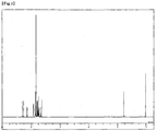
- the structure of the resulting brownish white powder was identified by NMR.
- the 1H-NMR measurement result is presented in FIG. 1 .
- the glass transition points of the compounds used in the present invention were determined using a high-sensitive differential scanning calorimeter DSC 3100S produced by Bruker AXS. Glass transition point Compound of Example 1 of the present invention 142.5°C
- the compounds used in the present invention have glass transition points of 100°C or higher, demonstrating that the compounds used in the present invention have a stable thin-film state.
- a 100 nm-thick vapor-deposited film was fabricated on an ITO substrate using the compounds used in the present invention, and the work function was measured using an atmosphere photoelectron spectrometer (Model AC-3 produced by Riken Keiki Co., Ltd.). Work function Compound of Example 1 of the present invention 5.44 eV
- the compounds used in the present invention have desirable energy levels compared to the work function 5.4 eV of common hole transport materials such as ⁇ -NPD and TPD, and thus possess desirable hole transportability.
- a 1.0 ⁇ 10 -5 mol/L 2-methyltetrahydrofuran solution was prepared for the compounds used in the present invention.
- the prepared solution was placed in a designated quartz tube, and aerated with pure nitrogen to remove the oxygen content.
- the tube was plugged with a septum rubber to prevent mixing with oxygen.
- the solution was irradiated with excitation light to measure the phosphorescence spectrum, using a spectrofluorometer FluoroMax-4 produced by Horiba Ltd.
- the wavelength of the first peak on the shorter wavelength side of the phosphorescence spectrum was taken, and the wavelength value was converted to light energy to calculate T 1 .
- T 1 Compound of Example 1 of the present invention 2.74 eV FIrpic 2.62 eV Ir(ppy) 3 2.42 eV CBP 2.56 eV ⁇ -NPD 2.29 eV
- the compounds used in the present invention have higher T 1 values than commonly used blue phosphorescent material FIrpic, green phosphorescent material Ir(ppy) 3 , commonly used host material CBP, and commonly used hole transport material ⁇ -NPD, and thus have sufficient capability for the confinement of the triplet excitons excited in the light emitting layer.
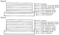
- the organic EL device as illustrated in FIG. 3 , was fabricated from a hole transport layer 4, a light emitting layer 5, a hole blocking layer 6, an electron transport layer 7, an electron injection layer 8, and a cathode (aluminum electrode) 9 successively formed by vapor deposition on a glass substrate 1 that had been provided beforehand with an ITO electrode as a transparent anode 2.
- the glass substrate 1 having ITO (thickness 150 nm) formed thereon was washed with an organic solvent, and subjected to an oxygen plasma treatment to wash the surface.
- the glass substrate with the ITO electrode was then installed in a vacuum vapor deposition apparatus, and the pressure was reduced to 0.001 Pa or less.
- the hole blocking layer 6 was then formed on the light emitting layer 5 by forming BCP in a thickness of 10 nm.
- the electron transport layer 7 was formed on the hole blocking layer 6 by forming Alq 3 in a thickness of 30 nm.
- the electron injection layer 8 was then formed on the electron transport layer 7 by forming lithium fluoride in a thickness of 0.5 nm.
- the cathode 9 was formed by vapor depositing aluminum in a thickness of 150 nm.
- Table 1 summarizes the results of the emission characteristics measurements performed by applying a DC voltage to the organic EL device.
- Example 6 For comparison, an organic EL device was fabricated under the same conditions used in Example 6, except that ⁇ -NPD was used as the material of the hole transport layer 4 of Example 6. The characteristics of the organic EL device thus fabricated were measured in an atmosphere at ordinary temperature. Table 1 summarizes the results of the emission characteristics measurements performed by applying a DC voltage to the organic EL device.
- Example 6 For comparison, an organic EL device was fabricated under the same conditions used in Example 6, except that Compound 54 of the following structural formula was used as the material of the hole transport layer 4 of Example 6. The characteristics of the organic EL device thus fabricated were measured in an atmosphere at ordinary temperature. Table 1 summarizes the results of the emission characteristics measurements performed by applying a DC voltage to the organic EL device.
- the organic EL device as illustrated in FIG. 4 , was fabricated from a hole injection layer 3, a hole transport layer 4, a light emitting layer 5, a hole blocking layer 6, an electron transport layer 7, an electron injection layer 8, and a cathode (aluminum electrode) 9 successively formed by vapor deposition on a glass substrate 1 that had been provided beforehand with an ITO electrode as a transparent anode 2.
- the glass substrate 1 having ITO (thickness 150 nm) formed thereon was washed with an organic solvent, and subjected to an oxygen plasma treatment to wash the surface.
- the glass substrate with the ITO electrode was then installed in a vacuum vapor deposition apparatus, and the pressure was reduced to 0.001 Pa or less.
- the hole transport layer 4 was formed on the hole injection layer 3 by forming the compound of Example 1 of the present invention (Compound 5) in a thickness of 30 nm.
- the hole blocking layer 6 was then formed on the light emitting layer 5 by forming BCP in a thickness of 10 nm.
- the electron transport layer 7 was formed on the hole blocking layer 6 by forming Alq 3 in a thickness of 30 nm.
- the electron injection layer 8 was then formed on the electron transport layer 7 by forming lithium fluoride in a thickness of 0.5 nm.
- the cathode 9 was formed by vapor depositing aluminum in a thickness of 150 nm.
- Table 1 summarizes the results of the emission characteristics measurements performed by applying a DC voltage to the organic EL device.
- Example 8 For comparison, an organic EL device was fabricated under the same conditions used in Example 8, except that ⁇ -NPD was used as the material of the hole transport layer 4 of Example 8. The characteristics of the organic EL device thus fabricated were measured in an atmosphere at ordinary temperature. Table 1 summarizes the results of the emission characteristics measurements performed by applying a DC voltage to the organic EL device.
- Example 1 For comparison, an organic EL device was fabricated under the same conditions used in Example 8, except that the Compound 54 was used as the material of the hole transport layer 4 of Example 8. The characteristics of the organic EL device thus fabricated were measured in an atmosphere at ordinary temperature. Table 1 summarizes the results of the emission characteristics measurements performed by applying a DC voltage to the organic EL device. Table 1 Hole injection layer material/hole transport layer material Voltage [V] (@ 10 mA/cm 2 ) Luminance [cd/m 2 ] (@ 10 mA/cm 2 ) Current efficiency [cd/A] (@ 10 mA/cm 2 ) Power efficiency [lm/W] (@ 10 mA/cm 2 ) Ex.
- V Voltage
- the driving voltage upon passing a current with a current density of 10 mA/cm 2 was 5.41 V for the compound of Example 1 of the present invention (Compound 5) used as the material of the hole transport layer, lower than 6.54 V or 5.89 V of when ⁇ -NPD or Compound 54 was used as the material of the hole transport layer. Further, the emission luminance, current efficiency, and power efficiency all greatly improved when the compound of Example 1 of the present invention (Compound 5) was used than when ⁇ -NPD and Compound 54 were used.
- the driving voltage lowered without affecting emission luminance, current efficiency, and power efficiency when Compound 55 was used as the material of the hole injection layer.
- the organic EL devices in which the compound of general formula (1) having a carbazole ring structure used in the present invention is used as the material of the hole transport layer can have improved emission luminance, luminous efficiency, and power efficiency, and a lower actual driving voltage, compared to the organic EL devices in which the known ⁇ -NPD and the Compound 54 were used as the material of the hole transport layer. It was also found that the driving voltage could be further lowered without affecting emission luminance, luminous efficiency, and power efficiency when an arylamine compound (the Compound 55) of a structure in which three or more triphenylamine structures are joined to each other within the molecule via a single bond or a divalent group that does not contain a heteroatom is used as the material of the hole injection layer.
- an arylamine compound the Compound 55
- the organic EL device produced by using the compound of general formula (1) having a carbazole ring structure can have high emission luminance, high luminous efficiency, and high power efficiency, and can have a low actual driving voltage to improve durability. There are potential applications for, for example, home electronic appliances and illuminations.
Landscapes
- Chemical & Material Sciences (AREA)
- Organic Chemistry (AREA)
- Physics & Mathematics (AREA)
- Engineering & Computer Science (AREA)
- Materials Engineering (AREA)
- Spectroscopy & Molecular Physics (AREA)
- Optics & Photonics (AREA)
- Crystallography & Structural Chemistry (AREA)
- Inorganic Chemistry (AREA)
- Electroluminescent Light Sources (AREA)
- Indole Compounds (AREA)
Claims (7)
- Dispositif électroluminescent organique comprenant une paire d'électrodes et une pluralité de couches organiques intercalées entre la paire d'électrodes et comprenant une couche émettrice de lumière contenant un matériau émettant de la lumière phosphorescente et une couche de transport de trous,
où un composé de la formule générale (1) suivante ayant une structure cyclique de type carbazole est utilisé comme constituant de la couche de transport de trous,
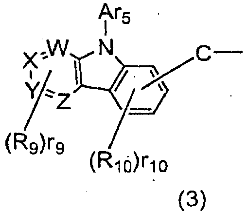
- Dispositif électroluminescent organique selon la revendication 1, dans lequel le composé de structure cyclique de type carbazole est utilisé comme constituant de la couche de transport de trous, où Ar2 dans la formule générale (1) est un groupe monovalent représenté par la formule générale (2) ou (3) suivante :


- Dispositif électroluminescent organique selon la revendication 1, comprenant une paire d'électrodes et une pluralité de couches organiques intercalées entre la paire d'électrodes et comprenant une couche émettrice de lumière contenant un matériau émettant de la lumière phosphorescente et une couche de transport de trous,
où un composé de la formule générale (1") suivante ayant une structure cyclique de type carbazole est utilisé comme constituant de la couche de transport de trous,

- Dispositif électroluminescent organique selon l'une quelconque des revendications 1 à 3, où la pluralité des couches organiques comprend une couche d'injection de trous, et la couche d'injection de trous contient un composé arylamine présentant une structure dans laquelle trois structures triphénylamine ou plus sont jointes les unes aux autres dans la molécule via un groupe bivalent qui ne contient pas d'hétéroatome, ou via une simple liaison.
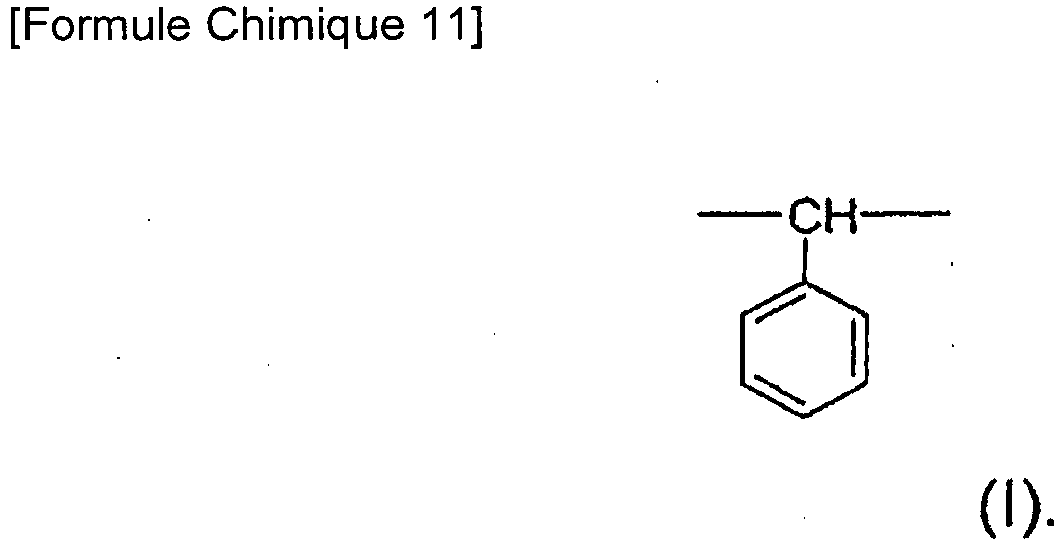
- Dispositif électroluminescent organique selon la revendication 4, où le composé arylamine présent dans la couche d'injection de trous et présentant une structure dans laquelle trois structures triphénylamine ou plus sont jointes les unes aux autres dans la molécule via un groupe bivalent qui ne contient pas d'hétéroatome, ou via une simple liaison, est un composé arylamine représenté par la formule générale (4) :


-CH2- (H)
- Dispositif électroluminescent organique comprenant une paire d'électrodes et une pluralité de couches organiques intercalées entre la paire d'électrodes et comprenant une couche émettrice de lumière contenant un matériau émettant de la lumière phosphorescente et une couche de transport de trous,
où un composé de la formule générale (1) ayant une structure cyclique de type carbazole tel que défini à la revendication 1 est utilisé comme constituant de la couche d'injection de trous, - Dispositif électroluminescent organique selon l'une quelconque des revendications 1 à 6, où le matériau émettant de la lumière phosphorescente est un complexe métallique qui contient de l'iridium ou du platine.
Applications Claiming Priority (2)
| Application Number | Priority Date | Filing Date | Title |
|---|---|---|---|
| JP2009244247 | 2009-10-23 | ||
| PCT/JP2010/006285 WO2011048822A1 (fr) | 2009-10-23 | 2010-10-22 | Élément électroluminescent organique |
Publications (3)
| Publication Number | Publication Date |
|---|---|
| EP2492986A1 EP2492986A1 (fr) | 2012-08-29 |
| EP2492986A4 EP2492986A4 (fr) | 2013-12-11 |
| EP2492986B1 true EP2492986B1 (fr) | 2016-06-15 |
Family
ID=43900066
Family Applications (1)
| Application Number | Title | Priority Date | Filing Date |
|---|---|---|---|
| EP10824674.5A Not-in-force EP2492986B1 (fr) | 2009-10-23 | 2010-10-22 | Élément électroluminescent organique |
Country Status (7)
| Country | Link |
|---|---|
| US (1) | US9306175B2 (fr) |
| EP (1) | EP2492986B1 (fr) |
| JP (1) | JPWO2011048822A1 (fr) |
| KR (2) | KR101843589B1 (fr) |
| CN (1) | CN102598343B (fr) |
| TW (1) | TWI549931B (fr) |
| WO (1) | WO2011048822A1 (fr) |
Families Citing this family (99)
| Publication number | Priority date | Publication date | Assignee | Title |
|---|---|---|---|---|
| EP2415769B1 (fr) | 2010-04-20 | 2015-10-28 | Idemitsu Kosan Co., Ltd. | Dérivé de bis-carbazole, matériau pour élément électroluminescent organique, et élément électroluminescent organique l'utilisant |
| WO2012001986A1 (fr) * | 2010-06-30 | 2012-01-05 | 保土谷化学工業株式会社 | Composé doté d'une structure cyclique de type carbazole et élément électroluminescent organique |
| EP2595208A1 (fr) * | 2010-07-13 | 2013-05-22 | Toray Industries, Inc. | Elément électroluminescent |
| KR20120104086A (ko) | 2010-08-31 | 2012-09-20 | 이데미쓰 고산 가부시키가이샤 | 질소 함유 방향족 복소환 유도체 및 이들을 이용한 유기 전계 발광 소자 |
| KR101478000B1 (ko) * | 2010-12-21 | 2015-01-05 | 롬엔드하스전자재료코리아유한회사 | 신규한 유기 발광 화합물 및 이를 채용하고 있는 유기 전계 발광 소자 |
| TWI538977B (zh) * | 2011-02-07 | 2016-06-21 | Idemitsu Kosan Co | A double carbazole derivative and an organic electroluminescent element using the same |
| WO2012108389A1 (fr) | 2011-02-07 | 2012-08-16 | 出光興産株式会社 | Dérivé de bis-carbazole ainsi qu'élément électroluminescent organique mettant en oeuvre celui-ci |
| CN103429570A (zh) | 2011-03-24 | 2013-12-04 | 出光兴产株式会社 | 双咔唑衍生物及使用其的有机电致发光元件 |
| KR101699583B1 (ko) * | 2011-05-27 | 2017-02-13 | 유니버셜 디스플레이 코포레이션 | 다성분 방출 층을 갖는 oled |
| US9705092B2 (en) | 2011-08-05 | 2017-07-11 | Universal Display Corporation | Phosphorescent organic light emitting devices combined with hole transport material having high operating stability |
| EP2790239B1 (fr) | 2011-12-05 | 2020-02-05 | Idemitsu Kosan Co., Ltd | Matériau pour élément électroluminescent organique et élément électroluminescent organique |
| US9386657B2 (en) | 2012-03-15 | 2016-07-05 | Universal Display Corporation | Organic Electroluminescent materials and devices |
| KR102235596B1 (ko) * | 2013-12-12 | 2021-04-05 | 삼성디스플레이 주식회사 | 유기 발광 소자 |
| US9929361B2 (en) | 2015-02-16 | 2018-03-27 | Universal Display Corporation | Organic electroluminescent materials and devices |
| US11056657B2 (en) | 2015-02-27 | 2021-07-06 | University Display Corporation | Organic electroluminescent materials and devices |
| US9478758B1 (en) * | 2015-05-08 | 2016-10-25 | Universal Display Corporation | Organic electroluminescent materials and devices |
| US9859510B2 (en) | 2015-05-15 | 2018-01-02 | Universal Display Corporation | Organic electroluminescent materials and devices |
| US10418568B2 (en) | 2015-06-01 | 2019-09-17 | Universal Display Corporation | Organic electroluminescent materials and devices |
| US11127905B2 (en) | 2015-07-29 | 2021-09-21 | Universal Display Corporation | Organic electroluminescent materials and devices |
| US10672996B2 (en) | 2015-09-03 | 2020-06-02 | Universal Display Corporation | Organic electroluminescent materials and devices |
| US20170229663A1 (en) | 2016-02-09 | 2017-08-10 | Universal Display Corporation | Organic electroluminescent materials and devices |
| US10236456B2 (en) | 2016-04-11 | 2019-03-19 | Universal Display Corporation | Organic electroluminescent materials and devices |
| US10672997B2 (en) | 2016-06-20 | 2020-06-02 | Universal Display Corporation | Organic electroluminescent materials and devices |
| US10862054B2 (en) | 2016-06-20 | 2020-12-08 | Universal Display Corporation | Organic electroluminescent materials and devices |
| US11482683B2 (en) | 2016-06-20 | 2022-10-25 | Universal Display Corporation | Organic electroluminescent materials and devices |
| US10608186B2 (en) | 2016-09-14 | 2020-03-31 | Universal Display Corporation | Organic electroluminescent materials and devices |
| US10680187B2 (en) | 2016-09-23 | 2020-06-09 | Universal Display Corporation | Organic electroluminescent materials and devices |
| US11196010B2 (en) | 2016-10-03 | 2021-12-07 | Universal Display Corporation | Organic electroluminescent materials and devices |
| US11011709B2 (en) | 2016-10-07 | 2021-05-18 | Universal Display Corporation | Organic electroluminescent materials and devices |
| US12317745B2 (en) | 2016-11-09 | 2025-05-27 | Universal Display Corporation | Organic electroluminescent materials and devices |
| US10680188B2 (en) | 2016-11-11 | 2020-06-09 | Universal Display Corporation | Organic electroluminescent materials and devices |
| US11780865B2 (en) | 2017-01-09 | 2023-10-10 | Universal Display Corporation | Organic electroluminescent materials and devices |
| WO2018168991A1 (fr) * | 2017-03-15 | 2018-09-20 | 保土谷化学工業株式会社 | Élément électroluminescent organique |
| US10844085B2 (en) | 2017-03-29 | 2020-11-24 | Universal Display Corporation | Organic electroluminescent materials and devices |
| US10944060B2 (en) | 2017-05-11 | 2021-03-09 | Universal Display Corporation | Organic electroluminescent materials and devices |
| US12098157B2 (en) | 2017-06-23 | 2024-09-24 | Universal Display Corporation | Organic electroluminescent materials and devices |
| US11228010B2 (en) | 2017-07-26 | 2022-01-18 | Universal Display Corporation | Organic electroluminescent materials and devices |
| US11744142B2 (en) | 2017-08-10 | 2023-08-29 | Universal Display Corporation | Organic electroluminescent materials and devices |
| US12180230B2 (en) | 2017-11-28 | 2024-12-31 | University Of Southern California | Carbene compounds and organic electroluminescent devices |
| EP3492480B1 (fr) | 2017-11-29 | 2021-10-20 | Universal Display Corporation | Matériaux et dispositifs électroluminescents organiques |
| US11937503B2 (en) | 2017-11-30 | 2024-03-19 | Universal Display Corporation | Organic electroluminescent materials and devices |
| WO2019142555A1 (fr) * | 2018-01-17 | 2019-07-25 | コニカミノルタ株式会社 | Film luminescent, dispositif électroluminescent organique et procédé de fabrication de dispositif électroluminescent organique |
| US11542289B2 (en) | 2018-01-26 | 2023-01-03 | Universal Display Corporation | Organic electroluminescent materials and devices |
| US11165028B2 (en) | 2018-03-12 | 2021-11-02 | Universal Display Corporation | Organic electroluminescent materials and devices |
| JP7421476B2 (ja) * | 2018-07-03 | 2024-01-24 | 保土谷化学工業株式会社 | 分子主鎖にターフェニル構造を含むトリアリールアミン高分子量化合物およびこれらの高分子量化合物を含む有機エレクトロルミネッセンス素子 |
| US12453279B2 (en) | 2018-08-22 | 2025-10-21 | Universal Display Corporation | Organic electroluminescent materials and devices |
| US11737349B2 (en) | 2018-12-12 | 2023-08-22 | Universal Display Corporation | Organic electroluminescent materials and devices |
| US11780829B2 (en) | 2019-01-30 | 2023-10-10 | The University Of Southern California | Organic electroluminescent materials and devices |
| US12477890B2 (en) | 2019-02-01 | 2025-11-18 | Universal Display Corporation | Organic electroluminescent materials and devices |
| KR102727031B1 (ko) * | 2019-02-22 | 2024-11-07 | 삼성디스플레이 주식회사 | 유기 발광 소자 |
| JP2020158491A (ja) | 2019-03-26 | 2020-10-01 | ユニバーサル ディスプレイ コーポレイション | 有機エレクトロルミネセンス材料及びデバイス |
| CN110437133B (zh) * | 2019-07-18 | 2022-10-14 | 中国科学院上海微系统与信息技术研究所 | 一种长寿命室温磷光材料及其制备方法和应用 |
| US12281128B2 (en) | 2019-07-30 | 2025-04-22 | Universal Display Corporation | Organic electroluminescent materials and devices |
| US12139501B2 (en) | 2019-08-16 | 2024-11-12 | Universal Display Corporation | Organic electroluminescent materials and devices |
| KR102889982B1 (ko) | 2019-08-23 | 2025-11-25 | 삼성디스플레이 주식회사 | 유기 전계 발광 소자 및 유기 전계 발광 소자용 다환 화합물 |
| US20210135130A1 (en) | 2019-11-04 | 2021-05-06 | Universal Display Corporation | Organic electroluminescent materials and devices |
| US12538698B2 (en) | 2020-01-06 | 2026-01-27 | Universal Display Corporation | Organic electroluminescent materials and devices |
| US12426495B2 (en) | 2020-01-28 | 2025-09-23 | Universal Display Corporation | Organic electroluminescent materials and devices |
| CN111470984B (zh) * | 2020-04-16 | 2022-12-13 | 苏州欧谱科显示科技有限公司 | 一种空穴传输材料及其制备方法和应用 |
| CN113896734A (zh) | 2020-07-06 | 2022-01-07 | 罗门哈斯电子材料韩国有限公司 | 有机电致发光化合物、多种主体材料和包含其的有机电致发光装置 |
| EP3937268B1 (fr) | 2020-07-10 | 2025-05-07 | Universal Display Corporation | Delo plasmoniques et émetteurs à dipôle vertical |
| CN114068825B (zh) * | 2020-07-29 | 2023-09-29 | 江苏三月科技股份有限公司 | 具有多空穴传输通道材料的有机电致发光器件及显示装置 |
| US12187748B2 (en) | 2020-11-02 | 2025-01-07 | Universal Display Corporation | Organic electroluminescent materials and devices |
| US20220158096A1 (en) | 2020-11-16 | 2022-05-19 | Universal Display Corporation | Organic electroluminescent materials and devices |
| US20220165967A1 (en) | 2020-11-24 | 2022-05-26 | Universal Display Corporation | Organic electroluminescent materials and devices |
| US12325717B2 (en) | 2020-11-24 | 2025-06-10 | Universal Display Corporation | Organic electroluminescent materials and devices |
| US12575316B2 (en) | 2021-02-03 | 2026-03-10 | Universal Display Corporation | Organic electroluminescent materials and devices |
| EP4060758A3 (fr) | 2021-02-26 | 2023-03-29 | Universal Display Corporation | Matériaux et dispositifs électroluminescents organiques |
| EP4723858A2 (fr) | 2021-02-26 | 2026-04-08 | Universal Display Corporation | Matériaux électroluminescents organiques et dispositifs |
| US12606582B2 (en) | 2021-03-05 | 2026-04-21 | Universal Display Corporation | Organic electroluminescent materials and devices |
| US12428599B2 (en) | 2021-03-09 | 2025-09-30 | Universal Display Corporation | Organic electroluminescent materials and devices |
| US20220298190A1 (en) | 2021-03-12 | 2022-09-22 | Universal Display Corporation | Organic electroluminescent materials and devices |
| US12421262B2 (en) | 2021-03-15 | 2025-09-23 | Universal Display Corporation | Organic electroluminescent materials and devices |
| US20220340607A1 (en) | 2021-04-05 | 2022-10-27 | Universal Display Corporation | Organic electroluminescent materials and devices |
| US12480042B2 (en) | 2021-04-09 | 2025-11-25 | Universal Display Corporation | Organic electroluminescent materials and devices |
| EP4075531A1 (fr) | 2021-04-13 | 2022-10-19 | Universal Display Corporation | Delo plasmoniques et émetteurs à dipôle vertical |
| US20220352478A1 (en) | 2021-04-14 | 2022-11-03 | Universal Display Corporation | Organic eletroluminescent materials and devices |
| US20230006149A1 (en) | 2021-04-23 | 2023-01-05 | Universal Display Corporation | Organic electroluminescent materials and devices |
| US20220407020A1 (en) | 2021-04-23 | 2022-12-22 | Universal Display Corporation | Organic electroluminescent materials and devices |
| US20230133787A1 (en) | 2021-06-08 | 2023-05-04 | University Of Southern California | Molecular Alignment of Homoleptic Iridium Phosphors |
| US12550611B2 (en) | 2021-08-03 | 2026-02-10 | Universal Display Corporation | Organic electroluminescent materials and devices |
| EP4151699A1 (fr) | 2021-09-17 | 2023-03-22 | Universal Display Corporation | Matériaux et dispositifs électroluminescents organiques |
| US12473318B2 (en) | 2021-10-08 | 2025-11-18 | Universal Display Corporation | Organic electroluminescent materials and devices |
| US12509628B2 (en) | 2021-12-16 | 2025-12-30 | Universal Display Corporation | Organic electroluminescent materials and devices |
| EP4231804A3 (fr) | 2022-02-16 | 2023-09-20 | Universal Display Corporation | Matériaux et dispositifs électroluminescents organiques |
| US20230292592A1 (en) | 2022-03-09 | 2023-09-14 | Universal Display Corporation | Organic electroluminescent materials and devices |
| US20230337516A1 (en) | 2022-04-18 | 2023-10-19 | Universal Display Corporation | Organic electroluminescent materials and devices |
| US20230389421A1 (en) | 2022-05-24 | 2023-11-30 | Universal Display Corporation | Organic electroluminescent materials and devices |
| EP4293001A1 (fr) | 2022-06-08 | 2023-12-20 | Universal Display Corporation | Matériaux électroluminescents organiques et dispositifs |
| US20240016051A1 (en) | 2022-06-28 | 2024-01-11 | Universal Display Corporation | Organic electroluminescent materials and devices |
| US20240107880A1 (en) | 2022-08-17 | 2024-03-28 | Universal Display Corporation | Organic electroluminescent materials and devices |
| US20240196730A1 (en) | 2022-10-27 | 2024-06-13 | Universal Display Corporation | Organic electroluminescent materials and devices |
| US20240188316A1 (en) | 2022-10-27 | 2024-06-06 | Universal Display Corporation | Organic electroluminescent materials and devices |
| US20240188419A1 (en) | 2022-10-27 | 2024-06-06 | Universal Display Corporation | Organic electroluminescent materials and devices |
| US20240188319A1 (en) | 2022-10-27 | 2024-06-06 | Universal Display Corporation | Organic electroluminescent materials and devices |
| US20240180025A1 (en) | 2022-10-27 | 2024-05-30 | Universal Display Corporation | Organic electroluminescent materials and devices |
| US20240247017A1 (en) | 2022-12-14 | 2024-07-25 | Universal Display Corporation | Organic electroluminescent materials and devices |
| US20250204238A1 (en) | 2023-12-15 | 2025-06-19 | Universal Display Corporation | Organic electroluminscent materials and devices |
| US20250204239A1 (en) | 2023-12-15 | 2025-06-19 | Universal Display Corporation | Organic electroluminescent materials and devices |
Family Cites Families (21)
| Publication number | Priority date | Publication date | Assignee | Title |
|---|---|---|---|---|
| JP3194657B2 (ja) | 1993-11-01 | 2001-07-30 | 松下電器産業株式会社 | 電界発光素子 |
| JP3828595B2 (ja) | 1994-02-08 | 2006-10-04 | Tdk株式会社 | 有機el素子 |
| JP3139321B2 (ja) | 1994-03-31 | 2001-02-26 | 東レ株式会社 | 発光素子 |
| JP3674133B2 (ja) | 1996-03-18 | 2005-07-20 | 東レ株式会社 | 発光素子 |
| JPH11144876A (ja) * | 1997-11-12 | 1999-05-28 | Toray Ind Inc | 発光素子 |
| US6998487B2 (en) * | 2001-04-27 | 2006-02-14 | Lg Chem, Ltd. | Double-spiro organic compounds and organic electroluminescent devices using the same |
| US6750608B2 (en) * | 2001-11-09 | 2004-06-15 | Konica Corporation | Organic electroluminescence element and display |
| CN100493286C (zh) | 2003-01-24 | 2009-05-27 | 出光兴产株式会社 | 有机电致发光元件 |
| KR100787425B1 (ko) | 2004-11-29 | 2007-12-26 | 삼성에스디아이 주식회사 | 페닐카바졸계 화합물 및 이를 이용한 유기 전계 발광 소자 |
| KR101097301B1 (ko) * | 2005-02-05 | 2011-12-23 | 삼성모바일디스플레이주식회사 | 백색발광소자 |
| KR101267114B1 (ko) * | 2005-04-18 | 2013-05-23 | 이데미쓰 고산 가부시키가이샤 | 방향족 트라이아민 화합물 및 그것을 이용한 유기 전기발광소자 |
| JP4904734B2 (ja) | 2005-07-20 | 2012-03-28 | 三菱化学株式会社 | 新規ピラゾール誘導体及びこれを含有する有機el素子 |
| CN101277822B (zh) | 2005-08-01 | 2012-01-25 | 日本先锋公司 | 有机膜热转印于其上的转印体的制造方法、有机膜热转印于其上的转印体 |
| JP5055818B2 (ja) | 2006-04-19 | 2012-10-24 | コニカミノルタホールディングス株式会社 | 有機エレクトロルミネッセンス素子材料、有機エレクトロルミネッセンス素子、表示装置及び照明装置 |
| WO2007148660A1 (fr) * | 2006-06-22 | 2007-12-27 | Idemitsu Kosan Co., Ltd. | Dispositif électroluminescent organique employant un dérivé d'arylamide contenant un hétérocyle |
| JP5133259B2 (ja) | 2006-11-24 | 2013-01-30 | 出光興産株式会社 | 芳香族アミン誘導体及びそれを用いた有機エレクトロルミネッセンス素子 |
| US7723722B2 (en) | 2007-03-23 | 2010-05-25 | Semiconductor Energy Laboratory Co., Ltd. | Organic compound, anthracene derivative, and light-emitting element, light-emitting device, and electronic device using anthracene derivative |
| KR20090028943A (ko) | 2007-09-17 | 2009-03-20 | (주)루디스 | 정공주입층/정공수송층 물질 및 이를 포함하는유기전계발광소자 |
| CN101515632A (zh) | 2008-02-14 | 2009-08-26 | 财团法人山形县产业技术振兴机构 | 有机发光元件 |
| JP4675413B2 (ja) | 2008-02-14 | 2011-04-20 | 財団法人山形県産業技術振興機構 | 有機発光素子 |
| KR101853143B1 (ko) * | 2009-08-28 | 2018-04-27 | 호도가야 가가쿠 고교 가부시키가이샤 | 카바졸환 구조를 가지는 화합물 및 유기 일렉트로 루미네센스 소자 |
-
2010
- 2010-10-22 WO PCT/JP2010/006285 patent/WO2011048822A1/fr not_active Ceased
- 2010-10-22 JP JP2011537148A patent/JPWO2011048822A1/ja active Pending
- 2010-10-22 US US13/503,186 patent/US9306175B2/en active Active
- 2010-10-22 KR KR1020127013076A patent/KR101843589B1/ko active Active
- 2010-10-22 EP EP10824674.5A patent/EP2492986B1/fr not_active Not-in-force
- 2010-10-22 KR KR1020177037033A patent/KR101869670B1/ko active Active
- 2010-10-22 CN CN201080047863.4A patent/CN102598343B/zh active Active
- 2010-10-25 TW TW099136330A patent/TWI549931B/zh active
Also Published As
| Publication number | Publication date |
|---|---|
| KR20180003625A (ko) | 2018-01-09 |
| TWI549931B (zh) | 2016-09-21 |
| CN102598343B (zh) | 2015-07-08 |
| KR101843589B1 (ko) | 2018-03-29 |
| CN102598343A (zh) | 2012-07-18 |
| US20120205642A1 (en) | 2012-08-16 |
| EP2492986A1 (fr) | 2012-08-29 |
| US9306175B2 (en) | 2016-04-05 |
| WO2011048822A1 (fr) | 2011-04-28 |
| JPWO2011048822A1 (ja) | 2013-03-07 |
| KR20120085827A (ko) | 2012-08-01 |
| KR101869670B1 (ko) | 2018-06-20 |
| TW201130788A (en) | 2011-09-16 |
| EP2492986A4 (fr) | 2013-12-11 |
Similar Documents
| Publication | Publication Date | Title |
|---|---|---|
| EP2492986B1 (fr) | Élément électroluminescent organique | |
| EP2471771B1 (fr) | Élément électroluminescent organique et composé ayant une structure à cycle carbazole | |
| US9306174B2 (en) | Organic electroluminescent device | |
| EP2679589B1 (fr) | Composés ayant une structure cyclique d'indolocarbazole et éléments électroluminescents organiques | |
| EP2589591A1 (fr) | Composé doté d'une structure cyclique de type carbazole et élément électroluminescent organique | |
| EP3010055B1 (fr) | Matière pour éléments électroluminescents organiques, élément électroluminescent organique utilisant cette matière et dispositif électronique | |
| EP2960958B1 (fr) | Élément électroluminescent organique | |
| EP3291323B1 (fr) | Élément électroluminescent organique | |
| EP3021372B1 (fr) | Élément électroluminescent organique | |
| EP2578572A1 (fr) | Composés avec structures cycliques d'acridane et éléments électroluminescents organiques | |
| US9905770B2 (en) | Compound having acridan ring structure, and organic electroluminescent device | |
| EP3605638B1 (fr) | Dispositif électroluminescent organique | |
| KR102931949B1 (ko) | 아릴아민 화합물 및 그것을 사용하는 전자 기기 | |
| EP4116393A1 (fr) | Élément électroluminescent organique | |
| EP3770158A1 (fr) | Composé comprenant une structure cyclique de benzimidazole et élément électroluminescent organique | |
| EP3139423A1 (fr) | Compose ayant une structure de noyau acridane et dispositif electroluminescent organique |
Legal Events
| Date | Code | Title | Description |
|---|---|---|---|
| PUAI | Public reference made under article 153(3) epc to a published international application that has entered the european phase |
Free format text: ORIGINAL CODE: 0009012 |
|
| 17P | Request for examination filed |
Effective date: 20120503 |
|
| AK | Designated contracting states |
Kind code of ref document: A1 Designated state(s): AL AT BE BG CH CY CZ DE DK EE ES FI FR GB GR HR HU IE IS IT LI LT LU LV MC MK MT NL NO PL PT RO RS SE SI SK SM TR |
|
| DAX | Request for extension of the european patent (deleted) | ||
| A4 | Supplementary search report drawn up and despatched |
Effective date: 20131112 |
|
| RIC1 | Information provided on ipc code assigned before grant |
Ipc: H01L 51/50 20060101AFI20131106BHEP Ipc: C07D 209/86 20060101ALI20131106BHEP Ipc: C09K 11/06 20060101ALI20131106BHEP |
|
| GRAP | Despatch of communication of intention to grant a patent |
Free format text: ORIGINAL CODE: EPIDOSNIGR1 |
|
| INTG | Intention to grant announced |
Effective date: 20160212 |
|
| RIN1 | Information on inventor provided before grant (corrected) |
Inventor name: TOGASHI, KAZUNORI Inventor name: KUSANO, SHIGERU Inventor name: TAKAHASHI, EIJI Inventor name: YOKOYAMA, NORIMASA Inventor name: NAGAOKA, MAKOTO |
|
| GRAS | Grant fee paid |
Free format text: ORIGINAL CODE: EPIDOSNIGR3 |
|
| GRAA | (expected) grant |
Free format text: ORIGINAL CODE: 0009210 |
|
| RIN1 | Information on inventor provided before grant (corrected) |
Inventor name: YOKOYAMA, NORIMASA Inventor name: KUSANO, SHIGERU Inventor name: TAKAHASHI, EIJI Inventor name: NAGAOKA, MAKOTO Inventor name: TOGASHI, KAZUNORI |
|
| RAP1 | Party data changed (applicant data changed or rights of an application transferred) |
Owner name: HODOGAYA CHEMICAL CO., LTD. |
|
| AK | Designated contracting states |
Kind code of ref document: B1 Designated state(s): AL AT BE BG CH CY CZ DE DK EE ES FI FR GB GR HR HU IE IS IT LI LT LU LV MC MK MT NL NO PL PT RO RS SE SI SK SM TR |
|
| REG | Reference to a national code |
Ref country code: CH Ref legal event code: EP Ref country code: GB Ref legal event code: FG4D |
|
| RIN2 | Information on inventor provided after grant (corrected) |
Inventor name: TOGASHI, KAZUNORI Inventor name: YOKOYAMA, NORIMASA Inventor name: TAKAHASHI, EIJI Inventor name: KUSANO, SHIGERU Inventor name: NAGAOKA, MAKOTO |
|
| REG | Reference to a national code |
Ref country code: IE Ref legal event code: FG4D |
|
| REG | Reference to a national code |
Ref country code: AT Ref legal event code: REF Ref document number: 806881 Country of ref document: AT Kind code of ref document: T Effective date: 20160715 |
|
| REG | Reference to a national code |
Ref country code: DE Ref legal event code: R096 Ref document number: 602010034104 Country of ref document: DE |
|
| REG | Reference to a national code |
Ref country code: FR Ref legal event code: PLFP Year of fee payment: 7 |
|
| REG | Reference to a national code |
Ref country code: LT Ref legal event code: MG4D |
|
| REG | Reference to a national code |
Ref country code: NL Ref legal event code: MP Effective date: 20160615 |
|
| PG25 | Lapsed in a contracting state [announced via postgrant information from national office to epo] |
Ref country code: NO Free format text: LAPSE BECAUSE OF FAILURE TO SUBMIT A TRANSLATION OF THE DESCRIPTION OR TO PAY THE FEE WITHIN THE PRESCRIBED TIME-LIMIT Effective date: 20160915 Ref country code: LT Free format text: LAPSE BECAUSE OF FAILURE TO SUBMIT A TRANSLATION OF THE DESCRIPTION OR TO PAY THE FEE WITHIN THE PRESCRIBED TIME-LIMIT Effective date: 20160615 Ref country code: FI Free format text: LAPSE BECAUSE OF FAILURE TO SUBMIT A TRANSLATION OF THE DESCRIPTION OR TO PAY THE FEE WITHIN THE PRESCRIBED TIME-LIMIT Effective date: 20160615 |
|
| REG | Reference to a national code |
Ref country code: AT Ref legal event code: MK05 Ref document number: 806881 Country of ref document: AT Kind code of ref document: T Effective date: 20160615 |
|
| PG25 | Lapsed in a contracting state [announced via postgrant information from national office to epo] |
Ref country code: GR Free format text: LAPSE BECAUSE OF FAILURE TO SUBMIT A TRANSLATION OF THE DESCRIPTION OR TO PAY THE FEE WITHIN THE PRESCRIBED TIME-LIMIT Effective date: 20160916 Ref country code: RS Free format text: LAPSE BECAUSE OF FAILURE TO SUBMIT A TRANSLATION OF THE DESCRIPTION OR TO PAY THE FEE WITHIN THE PRESCRIBED TIME-LIMIT Effective date: 20160615 Ref country code: NL Free format text: LAPSE BECAUSE OF FAILURE TO SUBMIT A TRANSLATION OF THE DESCRIPTION OR TO PAY THE FEE WITHIN THE PRESCRIBED TIME-LIMIT Effective date: 20160615 Ref country code: SE Free format text: LAPSE BECAUSE OF FAILURE TO SUBMIT A TRANSLATION OF THE DESCRIPTION OR TO PAY THE FEE WITHIN THE PRESCRIBED TIME-LIMIT Effective date: 20160615 Ref country code: LV Free format text: LAPSE BECAUSE OF FAILURE TO SUBMIT A TRANSLATION OF THE DESCRIPTION OR TO PAY THE FEE WITHIN THE PRESCRIBED TIME-LIMIT Effective date: 20160615 Ref country code: HR Free format text: LAPSE BECAUSE OF FAILURE TO SUBMIT A TRANSLATION OF THE DESCRIPTION OR TO PAY THE FEE WITHIN THE PRESCRIBED TIME-LIMIT Effective date: 20160615 |
|
| PG25 | Lapsed in a contracting state [announced via postgrant information from national office to epo] |
Ref country code: CZ Free format text: LAPSE BECAUSE OF FAILURE TO SUBMIT A TRANSLATION OF THE DESCRIPTION OR TO PAY THE FEE WITHIN THE PRESCRIBED TIME-LIMIT Effective date: 20160615 Ref country code: RO Free format text: LAPSE BECAUSE OF FAILURE TO SUBMIT A TRANSLATION OF THE DESCRIPTION OR TO PAY THE FEE WITHIN THE PRESCRIBED TIME-LIMIT Effective date: 20160615 Ref country code: EE Free format text: LAPSE BECAUSE OF FAILURE TO SUBMIT A TRANSLATION OF THE DESCRIPTION OR TO PAY THE FEE WITHIN THE PRESCRIBED TIME-LIMIT Effective date: 20160615 Ref country code: IS Free format text: LAPSE BECAUSE OF FAILURE TO SUBMIT A TRANSLATION OF THE DESCRIPTION OR TO PAY THE FEE WITHIN THE PRESCRIBED TIME-LIMIT Effective date: 20161015 Ref country code: IT Free format text: LAPSE BECAUSE OF FAILURE TO SUBMIT A TRANSLATION OF THE DESCRIPTION OR TO PAY THE FEE WITHIN THE PRESCRIBED TIME-LIMIT Effective date: 20160615 Ref country code: SK Free format text: LAPSE BECAUSE OF FAILURE TO SUBMIT A TRANSLATION OF THE DESCRIPTION OR TO PAY THE FEE WITHIN THE PRESCRIBED TIME-LIMIT Effective date: 20160615 |
|
| PGFP | Annual fee paid to national office [announced via postgrant information from national office to epo] |
Ref country code: FR Payment date: 20161007 Year of fee payment: 7 Ref country code: DE Payment date: 20161025 Year of fee payment: 7 |
|
| PG25 | Lapsed in a contracting state [announced via postgrant information from national office to epo] |
Ref country code: BE Free format text: LAPSE BECAUSE OF NON-PAYMENT OF DUE FEES Effective date: 20160615 Ref country code: SM Free format text: LAPSE BECAUSE OF FAILURE TO SUBMIT A TRANSLATION OF THE DESCRIPTION OR TO PAY THE FEE WITHIN THE PRESCRIBED TIME-LIMIT Effective date: 20160615 Ref country code: PT Free format text: LAPSE BECAUSE OF FAILURE TO SUBMIT A TRANSLATION OF THE DESCRIPTION OR TO PAY THE FEE WITHIN THE PRESCRIBED TIME-LIMIT Effective date: 20161017 Ref country code: ES Free format text: LAPSE BECAUSE OF FAILURE TO SUBMIT A TRANSLATION OF THE DESCRIPTION OR TO PAY THE FEE WITHIN THE PRESCRIBED TIME-LIMIT Effective date: 20160615 Ref country code: PL Free format text: LAPSE BECAUSE OF FAILURE TO SUBMIT A TRANSLATION OF THE DESCRIPTION OR TO PAY THE FEE WITHIN THE PRESCRIBED TIME-LIMIT Effective date: 20160615 Ref country code: AT Free format text: LAPSE BECAUSE OF FAILURE TO SUBMIT A TRANSLATION OF THE DESCRIPTION OR TO PAY THE FEE WITHIN THE PRESCRIBED TIME-LIMIT Effective date: 20160615 |
|
| REG | Reference to a national code |
Ref country code: DE Ref legal event code: R097 Ref document number: 602010034104 Country of ref document: DE |
|
| PLBE | No opposition filed within time limit |
Free format text: ORIGINAL CODE: 0009261 |
|
| STAA | Information on the status of an ep patent application or granted ep patent |
Free format text: STATUS: NO OPPOSITION FILED WITHIN TIME LIMIT |
|
| 26N | No opposition filed |
Effective date: 20170316 |
|
| PG25 | Lapsed in a contracting state [announced via postgrant information from national office to epo] |
Ref country code: DK Free format text: LAPSE BECAUSE OF FAILURE TO SUBMIT A TRANSLATION OF THE DESCRIPTION OR TO PAY THE FEE WITHIN THE PRESCRIBED TIME-LIMIT Effective date: 20160615 |
|
| REG | Reference to a national code |
Ref country code: CH Ref legal event code: PL |
|
| REG | Reference to a national code |
Ref country code: IE Ref legal event code: MM4A |
|
| PG25 | Lapsed in a contracting state [announced via postgrant information from national office to epo] |
Ref country code: CH Free format text: LAPSE BECAUSE OF NON-PAYMENT OF DUE FEES Effective date: 20161031 Ref country code: LI Free format text: LAPSE BECAUSE OF NON-PAYMENT OF DUE FEES Effective date: 20161031 |
|
| PG25 | Lapsed in a contracting state [announced via postgrant information from national office to epo] |
Ref country code: LU Free format text: LAPSE BECAUSE OF NON-PAYMENT OF DUE FEES Effective date: 20161022 Ref country code: SI Free format text: LAPSE BECAUSE OF FAILURE TO SUBMIT A TRANSLATION OF THE DESCRIPTION OR TO PAY THE FEE WITHIN THE PRESCRIBED TIME-LIMIT Effective date: 20160615 |
|
| PG25 | Lapsed in a contracting state [announced via postgrant information from national office to epo] |
Ref country code: IE Free format text: LAPSE BECAUSE OF NON-PAYMENT OF DUE FEES Effective date: 20161022 |
|
| REG | Reference to a national code |
Ref country code: DE Ref legal event code: R119 Ref document number: 602010034104 Country of ref document: DE |
|
| PG25 | Lapsed in a contracting state [announced via postgrant information from national office to epo] |
Ref country code: CY Free format text: LAPSE BECAUSE OF FAILURE TO SUBMIT A TRANSLATION OF THE DESCRIPTION OR TO PAY THE FEE WITHIN THE PRESCRIBED TIME-LIMIT Effective date: 20160615 Ref country code: HU Free format text: LAPSE BECAUSE OF FAILURE TO SUBMIT A TRANSLATION OF THE DESCRIPTION OR TO PAY THE FEE WITHIN THE PRESCRIBED TIME-LIMIT; INVALID AB INITIO Effective date: 20101022 |
|
| PG25 | Lapsed in a contracting state [announced via postgrant information from national office to epo] |
Ref country code: MC Free format text: LAPSE BECAUSE OF FAILURE TO SUBMIT A TRANSLATION OF THE DESCRIPTION OR TO PAY THE FEE WITHIN THE PRESCRIBED TIME-LIMIT Effective date: 20160615 Ref country code: TR Free format text: LAPSE BECAUSE OF FAILURE TO SUBMIT A TRANSLATION OF THE DESCRIPTION OR TO PAY THE FEE WITHIN THE PRESCRIBED TIME-LIMIT Effective date: 20160615 Ref country code: MT Free format text: LAPSE BECAUSE OF NON-PAYMENT OF DUE FEES Effective date: 20161031 Ref country code: MK Free format text: LAPSE BECAUSE OF FAILURE TO SUBMIT A TRANSLATION OF THE DESCRIPTION OR TO PAY THE FEE WITHIN THE PRESCRIBED TIME-LIMIT Effective date: 20160615 |
|
| REG | Reference to a national code |
Ref country code: FR Ref legal event code: ST Effective date: 20180629 |
|
| PG25 | Lapsed in a contracting state [announced via postgrant information from national office to epo] |
Ref country code: DE Free format text: LAPSE BECAUSE OF NON-PAYMENT OF DUE FEES Effective date: 20180501 Ref country code: BG Free format text: LAPSE BECAUSE OF FAILURE TO SUBMIT A TRANSLATION OF THE DESCRIPTION OR TO PAY THE FEE WITHIN THE PRESCRIBED TIME-LIMIT Effective date: 20160615 |
|
| PG25 | Lapsed in a contracting state [announced via postgrant information from national office to epo] |
Ref country code: FR Free format text: LAPSE BECAUSE OF NON-PAYMENT OF DUE FEES Effective date: 20171031 |
|
| PG25 | Lapsed in a contracting state [announced via postgrant information from national office to epo] |
Ref country code: AL Free format text: LAPSE BECAUSE OF FAILURE TO SUBMIT A TRANSLATION OF THE DESCRIPTION OR TO PAY THE FEE WITHIN THE PRESCRIBED TIME-LIMIT Effective date: 20160615 |
|
| PGFP | Annual fee paid to national office [announced via postgrant information from national office to epo] |
Ref country code: GB Payment date: 20221020 Year of fee payment: 13 |
|
| GBPC | Gb: european patent ceased through non-payment of renewal fee |
Effective date: 20231022 |
|
| PG25 | Lapsed in a contracting state [announced via postgrant information from national office to epo] |
Ref country code: GB Free format text: LAPSE BECAUSE OF NON-PAYMENT OF DUE FEES Effective date: 20231022 |
|
| PG25 | Lapsed in a contracting state [announced via postgrant information from national office to epo] |
Ref country code: GB Free format text: LAPSE BECAUSE OF NON-PAYMENT OF DUE FEES Effective date: 20231022 |