EP2495754A2 - Herstellungsverfahren eines integrierten Schaltkreises, das auf der Bildung von Leitungen und Gräben beruht - Google Patents
Herstellungsverfahren eines integrierten Schaltkreises, das auf der Bildung von Leitungen und Gräben beruht Download PDFInfo
- Publication number
- EP2495754A2 EP2495754A2 EP12155129A EP12155129A EP2495754A2 EP 2495754 A2 EP2495754 A2 EP 2495754A2 EP 12155129 A EP12155129 A EP 12155129A EP 12155129 A EP12155129 A EP 12155129A EP 2495754 A2 EP2495754 A2 EP 2495754A2
- Authority
- EP
- European Patent Office
- Prior art keywords
- layer
- patterns
- hard mask
- photosensitive
- etching
- Prior art date
- Legal status (The legal status is an assumption and is not a legal conclusion. Google has not performed a legal analysis and makes no representation as to the accuracy of the status listed.)
- Withdrawn
Links
Images


Classifications
-
- H—ELECTRICITY
- H10—SEMICONDUCTOR DEVICES; ELECTRIC SOLID-STATE DEVICES NOT OTHERWISE PROVIDED FOR
- H10P—GENERIC PROCESSES OR APPARATUS FOR THE MANUFACTURE OR TREATMENT OF DEVICES COVERED BY CLASS H10
- H10P50/00—Etching of wafers, substrates or parts of devices
- H10P50/71—Etching of wafers, substrates or parts of devices using masks for conductive or resistive materials
-
- H—ELECTRICITY
- H10—SEMICONDUCTOR DEVICES; ELECTRIC SOLID-STATE DEVICES NOT OTHERWISE PROVIDED FOR
- H10D—INORGANIC ELECTRIC SEMICONDUCTOR DEVICES
- H10D64/00—Electrodes of devices having potential barriers
- H10D64/01—Manufacture or treatment
- H10D64/013—Manufacture or treatment of electrodes having a conductor capacitively coupled to a semiconductor by an insulator
- H10D64/01302—Manufacture or treatment of electrodes having a conductor capacitively coupled to a semiconductor by an insulator the insulator being formed after the semiconductor body, the semiconductor being silicon
- H10D64/01304—Manufacture or treatment of electrodes having a conductor capacitively coupled to a semiconductor by an insulator the insulator being formed after the semiconductor body, the semiconductor being silicon characterised by the conductor
- H10D64/01326—Aspects related to lithography, isolation or planarisation of the conductor
-
- H—ELECTRICITY
- H10—SEMICONDUCTOR DEVICES; ELECTRIC SOLID-STATE DEVICES NOT OTHERWISE PROVIDED FOR
- H10P—GENERIC PROCESSES OR APPARATUS FOR THE MANUFACTURE OR TREATMENT OF DEVICES COVERED BY CLASS H10
- H10P74/00—Testing or measuring during manufacture or treatment of wafers, substrates or devices
- H10P74/20—Testing or measuring during manufacture or treatment of wafers, substrates or devices characterised by the properties tested or measured, e.g. structural or electrical properties
- H10P74/203—Structural properties, e.g. testing or measuring thicknesses, line widths, warpage, bond strengths or physical defects
-
- H—ELECTRICITY
- H10—SEMICONDUCTOR DEVICES; ELECTRIC SOLID-STATE DEVICES NOT OTHERWISE PROVIDED FOR
- H10P—GENERIC PROCESSES OR APPARATUS FOR THE MANUFACTURE OR TREATMENT OF DEVICES COVERED BY CLASS H10
- H10P74/00—Testing or measuring during manufacture or treatment of wafers, substrates or devices
- H10P74/23—Testing or measuring during manufacture or treatment of wafers, substrates or devices characterised by multiple measurements, corrections, marking or sorting processes
-
- H—ELECTRICITY
- H10—SEMICONDUCTOR DEVICES; ELECTRIC SOLID-STATE DEVICES NOT OTHERWISE PROVIDED FOR
- H10P—GENERIC PROCESSES OR APPARATUS FOR THE MANUFACTURE OR TREATMENT OF DEVICES COVERED BY CLASS H10
- H10P76/00—Manufacture or treatment of masks on semiconductor bodies, e.g. by lithography or photolithography
- H10P76/40—Manufacture or treatment of masks on semiconductor bodies, e.g. by lithography or photolithography of masks comprising inorganic materials
- H10P76/408—Manufacture or treatment of masks on semiconductor bodies, e.g. by lithography or photolithography of masks comprising inorganic materials characterised by their sizes, orientations, dispositions, behaviours or shapes
- H10P76/4085—Manufacture or treatment of masks on semiconductor bodies, e.g. by lithography or photolithography of masks comprising inorganic materials characterised by their sizes, orientations, dispositions, behaviours or shapes characterised by the processes involved to create the masks
Definitions
- the present invention relates to a method for manufacturing electronic components on a semiconductor substrate.
- it relates to photolithography processes employing successive etching steps of patterns in a layer called "hard mask” (“hard mask”) deposited on a target layer.
- Photolithography processes involve etching patterns using a layer of a photosensitive material, such as a photoresist, deposited on a target layer to be treated formed on a substrate.
- a layer called "hard mask” may be deposited on the target layer before depositing the photoresist layer.
- the pattern to be transferred to the target layer is then transferred to the resin layer by photolithography, followed by etching to the hard mask layer and the target layer.
- a transfer of patterns to the photoresist layer generally involves exposing the layer in a photolithography machine to a particle beam through a mask having the patterns to be transferred, and then removing the exposed portions (in the case of a positive resin) or unexposed (in the case of a negative resin) using a developing solvent.
- the minimum size of the patterns that can be transferred to a photosensitive layer is called the "critical dimension" (CD) and corresponds, for example, to the width of a pattern line.
- the critical dimension depends on characteristics of the photolithography exposure machine and in particular the optical projection device, and the characteristics of the exposure, the development and the photosensitive material used.
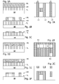
- FIGS. 1A to 1F and 2A to 2C Such a multi-transfer pattern photolithography process is illustrated by the FIGS. 1A to 1F and 2A to 2C .
- the Figures 1A to 1F represent in cross section a portion of a multilayer structure formed from a wafer made of a semiconductor material ("wafer"), at different stages of a photolithography process.
- the FIGS. 2A to 2C represent in top view a portion of the multilayer structure at some of the steps of the photolithography process.
- the multilayer structure comprises a substrate SB on which a target layer TL is formed.
- the target layer TL is covered with a hard mask layer HM, and the HM layer is covered with a layer of photoresist PR.
- line patterns formed on a first mask were transferred to the PR layer by a photolithography machine.
- the Figure 2A presents the shape of the line patterns transferred to the PR layer.
- the line patterns form parallel lines L1, L2, L3, of which two adjacent lines L1, L2 are connected by a bridge.
- the lines L1, L2, L3 formed in the treated layer have a width D that can correspond to the critical dimension of the photolithography treatment. This width is decisive on the electrical performance of components that will be formed by the line patterns in the target layer TL.
- the line patterns were transferred to the HM layer by etching treatment and the PR layer was removed.
- the HM layer is again covered with a layer of photoresist PR '.
- cutting patterns formed on a second mask were transferred to the PR 'layer by the photolithography machine.
- the Figure 2B presents the shape of the cutting patterns transferred to the PR 'layer.
- the cutting patterns form rectangular trenches R1, R2 provided for cutting lines L1, L2, L3 which have been formed in the HM layer.
- the trenches R1, R2 have a width D1 which may be greater than the critical dimension CD.
- the cutting patterns have dimensions that are not critical to the electrical performance of the components formed by the line patterns. It is simply important that the cutting patterns intersect the lines at desired locations to form separate electronic components.
- the HM layer was etched to the shape of the patterns transferred in the PR 'layer, the PR' layer was removed, and the TL target layer was etched to the shape of the patterns transferred in the HM layer.
- the Figure 2C presents the shape of the patterns thus formed in the layers HM and TL. These patterns correspond to lines L1, L2, L3 to which rectangular areas R1, R2 have been removed. The hard mask layer HM can then be completely removed.
- Embodiments are directed to a method of etching a target layer, comprising steps of: depositing a hard mask layer on a target layer and on the hard mask layer, a first layer of a photosensitive material, exposing the first layer light-sensitive layer with a particle beam through a first mask for transferring first patterns, forming the first patterns in the photosensitive layer, transferring the first patterns in the hard mask layer by etching this layer through the first layer photosensitive, depositing on the hard mask layer a second layer of photosensitive material, exposing the second photosensitive layer to a particle beam through a second mask to transfer second patterns, forming the second patterns in the second photosensitive layer , transferring the second patterns into the hard mask layer by etching this layer through the second e photosensitive layer, and transfer the first and second patterns in the target layer by etching this layer through the hard mask layer, the second patterns forming lines in the hard mask layer, and the first patterns forming trenches cutting the lines in the hard mask layer.
- the method comprises the steps of: depositing on the etched hard mask layer a third layer made of a photosensitive material, expose the third light-sensitive layer to a particle beam through a third mask for transferring third patterns, forming the third patterns in the third photosensitive layer, and transferring the third patterns in the hard mask layer by etching this layer through the third light-sensitive layer, the target layer being etched while receiving the first, second and third patterns formed in the hard mask layer, the third patterns forming lines cut by the first patterns.
- one or each of the photosensitive layers is deposited directly on the hard mask layer, previously etched or not, the photosensitive layer having a reflection coefficient of the particle beam of less than 1%, and an upper face. flat, and covers the hard mask layer without trapping gas bubbles.
- an additional layer is deposited directly on the hard mask layer, previously etched or not, one or each of the photosensitive layers being deposited on the additional layer, the method comprising a step of etching the additional layer. for transferring the patterns formed in the photosensitive layer to the additional layer.
- the additional layer has a particle beam reflection coefficient of less than 1%, and a planar upper face, and covers the hard mask layer without trapping gas bubbles.
- the upper surface of one or each of the photosensitive layers has a height variation of less than 20%, and preferably less than 15%.
- one or each of the photosensitive layers is deposited on a second hard mask layer, the second hard mask layer being deposited on the additional layer, the method comprising a step of etching the second mask layer. hard to transfer the patterns formed in the photosensitive layer to the hard mask layer.
- the target layer is a layer provided for forming gates of CMOS transistors.
- step S1 a hard mask layer HM and a layer of a photosensitive material PR are deposited successively on a target layer TL.
- the Figure 4A represents a multilayer structure that can be obtained at the end of step S1.
- the multilayer structure comprises the target layer TL to be processed by the photolithography method, the target layer being formed on a substrate SB.
- the layer TL is covered by the layer HM, and the layer HM is covered with the layer PR.
- step S2 the PR layer is subjected to a particle beam (photons, electrons, ...) through an MSK1 mask.
- Step S3 is a development step during which the exposed (or unexposed) portions are removed by the photolithography machine through the MSK1 mask.
- the Figure 4B represents the multilayer structure after the transfer of the patterns of the mask MSK1 to the PR layer.
- the Figure 5A represents the shape of the patterns transferred to the PR layer.
- the patterns transferred by the mask MSK1 to the PR layer are cutting patterns for forming trenches in the hard mask layer HM.
- the cutting patterns have a minimum dimension that may be larger than the critical dimension of the photolithography process.
- the patterns of the mask MSK1 transferred into the PR layer comprise two trenches R1, R2 of rectangular shape whose width D1 may be greater than the critical dimension of the photolithography machine used.
- step S4 is a metrology step for controlling the quality of the transfer of the mask MSK1 to the PR layer. If, on a batch of platelets, the patterns R1, R2 have larger or smaller dimensions than desired dimensions, the photolithography treatment performed in steps S2, S3 can be readjusted for a next batch of platelets. This readjustment as a function of measurement forms a control loop (here feedback type also called “Run to Run") which improves the overall quality of batches of platelets so produced.
- the measurements obtained in step S4 on a given batch of platelets can also be used to adjust on the same batch of platelets the etching parameters of the hard mask layer in the next step S5. This readjustment performed at a next step (commonly called "Feed Forward"), based on measurements obtained in a previous step, is also important for the control of manufacturing processes.
- step S5 the HM layer is etched through the PR layer to transfer the patterns formed in the PR layer to the HM layer, and the PR layer is removed.
- the figure 4C represents the multilayer structure to the outcome of step S5.
- step S6 is a metrology step for controlling the dimensions of the patterns transferred to the hard mask layer HM. If the measurements obtained in step S6 are not satisfactory, the photolithography treatment performed in steps S2, S3 can be readjusted for a next batch of platelets.
- step S7 a new layer of photoresist PR 'is deposited on the HM layer which has been etched in step S5.
- the figure 4D represents the multilayer structure at the end of step S7.
- This step is for example carried out by centrifugation, by depositing liquid resin in the center of a wafer made of a semiconductor material forming the substrate SB, and rotating the wafer.
- step S8 the resin layer PR 'is subjected to a particle beam (photons, electrons, %) through an MSK2 mask.
- Step S9 is a development step during which the exposed (or unexposed) portions are removed by the photolithography machine through the MSK2 mask.
- the figure 4E represents the multilayer structure after the transfer of the patterns of the mask MSK2 to the layer PR '.
- the patterns transferred by the mask MSK2 to the PR 'layer are line patterns having a minimum dimension which may be equal to the critical dimension of the photolithography treatment.
- the Figure 5B represents the shape of the patterns transferred to the PR 'layer. On the Figure 5B , the transferred patterns have lines L1, L2, L3, among which the adjacent lines L1, L2 are connected by a bridge.
- the lines L1, L2, L3 formed in the PR 'layer have a width D2 which may be equal to the critical dimension of the photolithography treatment. This width is decisive on the electrical performance of components that will be formed by the line patterns in the target layer TL. On the contrary, the cutting patterns R1, R2 have dimensions that are not critical to the electrical performance of the components formed by the line patterns. It is simply important that the cutting patterns intersect the lines at desired locations to form separate electronic components.
- step S10 is a metrology step for controlling the dimensions of the patterns transferred to the PR 'layer. If at step S10, the dimensions of the patterns transferred in the PR layer were greater than or equal to less than desired dimensions, the photolithography treatment performed in steps S8, S9 can be readjusted for a next batch of platelets.
- step S11 the HM layer is etched to the shape of the patterns transferred in the PR 'layer, and the PR' layer is removed. If in step S10, the dimensions of the transferred patterns in the PR 'layer were larger than desired dimensions, the etching process of the HM layer can be extended. The target layer TL is then etched to the shape of the patterns R1, R2, L1, L2, L3 transferred to the HM layer.
- the figure 4F represents the multilayer structure at the end of the etching process in step S11.
- the Figure 5C presents the shape of the patterns formed in the HM and TL layers. These patterns correspond to lines L1, L2, L3 to which rectangular areas R1, R2 have been removed. The hard mask layer HM can then be completely removed.
- the following step S12 is a metrology step to determine in particular whether the dimensions of the transferred patterns in the target layer TL correspond to those desired. If the measurements obtained in step S12 are not satisfactory, the photolithography treatments carried out in steps S2, S3 and S8, S9 can be readjusted for a following batch of platelets.
- the etching treatments of the hard mask layer have a reducing effect on the critical dimension of the patterns formed in this layer and therefore in the target layer.
- the L1, L2, L3 patterns transferred in the PR 'layer have a critical dimension of 52 nm, and when they are transferred into the target layer TL, they can reach a dimension of 34 nm.
- the metrology steps are for example carried out using a scanning electron microscope SEM (Scanning Electron Microscope), or by scalerometry.
- SEM scanning Electron Microscope
- the patterns thus formed in the target layer TL make it possible, for example, to produce gates of CMOS transistors, the layer TL then being of monocrystalline polysilicon.
- the width D2 of the lines L1, L2, L3 corresponds to the length of the gates of the transistors thus formed.
- L1, L2, L3 patterns in the hard mask layer HM is not impaired by the presence of the trenches R1, R2 formed beforehand in the HM layer. Indeed, for a photosensitive layer to be correctly exposed, it is necessary that the surface to be exposed is very flat. The deposition of a photosensitive layer on the slightest relief is therefore to be avoided in particular when the structures to be formed are very critical as regards their dimensions. In the present case, the deposition of the photosensitive layer PR 'on the trenches R1, R2 formed in the HM layer was therefore to be avoided.
- the deposition on the hard mask layer HM of a layer having planarizing and anti-reflective properties may be sufficient to overcome the presence of relief (trenches R1, R2) in the HM layer.
- the resin used to form the PR 'layer may be chosen to cover the HM layer by penetrating the trenches R1, R2 formed in step S5 without trapping gas bubbles, and have a sufficiently flat and anti -reflective, after its deposition on the HM layer to not affect the subsequent photolithography and etching of the hard mask layer HM.
- the layer deposited on the hard mask layer HM it is desirable for the layer deposited on the hard mask layer HM to have sufficient planarizing properties so that its upper surface has, especially on either side of the edge of a trench pattern R1, R2, a variation its height less than 20%, and preferably less than 15%, this variation being expressed as a percentage of the depth of field of the photolithography treatment employed.
- a photolithography treatment having a depth of field of 120 nm and a hard mask of 30 nm thickness
- the local variations in height induced by the presence of the trenches would represent 25% of the depth of field.
- the upper surface of the resin PR ' would also have local variations representing 25% of the depth of field, which is unacceptable in practice for a critical photolithography step.
- a layer of resin making it possible to reduce to less than 20 nm at its upper surface, the variations of height of 30 nm induced at its bottom surface through trenches, reduces local variations in height of the top surface of the resin to less than 17% of the depth of field, which is acceptable.
- the method which has just been described has the advantage of successively carrying out critical photolithography and etching processes (steps S7, S8, S9 and S11), that is to say determinants on the electrical performance of the electronic components produced. .
- the photolithography and trench etching process was carried out between the photolithography process and the final etching of the electrically critical structures.
- This advantage offers the possibility of carrying out critical photolithography and etching treatments without having to change the engraving machine.
- This also makes it possible to optimally implement "Feed Forward" type control loops.
- This method also has the advantage of having to perform only two critical dimensional checks instead of three as in the method of the prior art. Indeed, the dimensional control performed in step S4 does not concern critical reasons with respect to the formation of electronic components.
- the photosensitive resins employed have planarizing and anti-reflective properties.
- the planarizing and anti-reflective properties of the photosensitive resins are generally insufficient to reach critical dimensions of less than 100 nm.
- the anti-reflective property is characterized by a reflection coefficient of the particle beam emitted by the photolithography machine less than 1%, or 0.5%. This property can be obtained using an anti-reflective coating BARC ("Bottom Anti Reflective Coating") formed under the layer of resin PR 'and possibly under the PR layer.
- BARC Bottom Anti Reflective Coating
- the BARC coating can be produced by coating an antireflective resin, or by deposition (CVD - Chemical Vapor Deposition, PECVD - Plasma-Enhanced Chemical Vapor Deposition, ...) of an organic layer (for example amorphous carbon) and / or a dielectric layer (for example silicon oxide SiO 2 , silicon nitride Si 3 N 4 , ).
- CVD - Chemical Vapor Deposition PECVD - Plasma-Enhanced Chemical Vapor Deposition, ...) of an organic layer (for example amorphous carbon) and / or a dielectric layer (for example silicon oxide SiO 2 , silicon nitride Si 3 N 4 , .
- FIG. 6 represents a multilayer structure that can be formed in steps S1 and S7.
- the hard mask layer HM deposited on the target layer TL is covered with an AL layer made of an anti-reflective and planarizing material, for example based on carbon.
- the layer AL is covered with a hard mask layer HM1, on which is deposited the photoresist layer PR, PR '.
- the HM and HM1 layers may be formed of silicon oxide, silicon nitride, or TiN titanium nitride.
- the AL layer is made of a material capable of covering the HM layer by penetrating into the trenches formed in step S5 without trapping gas bubbles, and having a planar upper face after its deposition on the HM layer.
- the AL layer also has antireflective properties, that is to say a reflection coefficient of the particle beam emitted by the photolithography machine less than 1%.
- the AL layer can comprise an organic film (for example carbon) deposited by centrifugation or by CVD or PECVD.
- the layers AL, HM1 and PR are reformed with each transfer of mask patterns to the HM layer.
- the different layers deposited on the target layer TL may be formed by PVD (Physical Vapor Deposition) or CVD, or by centrifugation.
- the development processes of the PR, PR 'photosensitive layers after exposure, and the etching treatments of the hard mask layers HM, HM1, of the AL layer and of the target layer TL, are adapted to the dimensions to be obtained and to the materials to be etched. , and can implement known techniques.
- steps S7 to S10 can be repeated with masks forming complementary patterns such that the combination of masks can form high density structures.
- These high density structures are generally cut after formation in the hard mask layer and before their final transfer into the layer to be etched.
- the steps of forming areas to be removed (trenches) in the hard mask layer are performed prior to the multiple steps of forming the high density structures (lines).
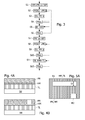
- the Figures 7A to 7E illustrate different steps of a photolithography treatment for successively transferring the patterns of three masks. As previously, steps S1 to S6, corresponding to Figures 4A to 4C , are performed to transfer the patterns R1, R2 represented on the Figure 5A to the hard mask layer HM.
- a new layer of a photosensitive material PR ' is deposited on the HM layer.
- Reasons such as those depicted on the Figures 7A, 8A are transferred to the PR 'layer.
- the patterns comprise three parallel lines L4, L5, L6 whose width may be equal to the critical dimension of the photolithography treatment.
- lines L5, L6, L7 form trenches in the PR 'layer.
- the patterns formed in the PR 'layer are then transferred into the HM layer, as illustrated by the Figure 7B .
- the HM layer is excavated both by the trenches corresponding to the lines L4, L5, L6 and the trenches corresponding to the rectangular zones R1, R2 ( Figure 5A ).
- the new transferred patterns comprise parallel lines L7, L8, L9 which are transferred into the PR layer "forming trenches between the lines L4, L5, L6, the PR layer" makes it possible to transfer the patterns L7, L8, L9 to the HM layer as shown on the Figures 7D and 8D .
- the HM layer collects trenches R1, R2, and lines L4 to L9.
- the target layer TL is then etched to the patterns formed in the HM layer.
- the lines between the trenches formed by lines L4 to L9 form, for example, gates of CMOS transistors.
- the present invention is capable of various alternative embodiments and various applications.
- the invention is not limited to the etching of a polysilicon layer to form transistors gates, but can be applied to the etching of hard mask layers for doping zones of the substrate or of a layer of semiconductor material, or etchings of various layers formed on a wafer of a semiconductor material.
- the various layers presented on the figure 6 can be deposited only to perform the second etching of the hard mask layer HM and any subsequent etchings.
- the present invention is also not limited to rectangular-shaped patterns for line and cut patterns. Other more complex polygonal pattern shapes can of course be transferred to the hard mask layer and the target layer.
Landscapes
- Drying Of Semiconductors (AREA)
- Exposure And Positioning Against Photoresist Photosensitive Materials (AREA)
- Photosensitive Polymer And Photoresist Processing (AREA)
Applications Claiming Priority (1)
| Application Number | Priority Date | Filing Date | Title |
|---|---|---|---|
| FR1100662A FR2972293A1 (fr) | 2011-03-04 | 2011-03-04 | Procédé de fabrication d'un circuit intégré sur la formation de lignes et de tranches |
Publications (2)
| Publication Number | Publication Date |
|---|---|
| EP2495754A2 true EP2495754A2 (de) | 2012-09-05 |
| EP2495754A3 EP2495754A3 (de) | 2013-12-25 |
Family
ID=45562252
Family Applications (1)
| Application Number | Title | Priority Date | Filing Date |
|---|---|---|---|
| EP12155129.5A Withdrawn EP2495754A3 (de) | 2011-03-04 | 2012-02-13 | Herstellungsverfahren eines integrierten Schaltkreises, das auf der Bildung von Leitungen und Gräben beruht |
Country Status (3)
| Country | Link |
|---|---|
| US (1) | US20120225560A1 (de) |
| EP (1) | EP2495754A3 (de) |
| FR (1) | FR2972293A1 (de) |
Families Citing this family (4)
| Publication number | Priority date | Publication date | Assignee | Title |
|---|---|---|---|---|
| CN103309165A (zh) * | 2012-03-09 | 2013-09-18 | 中芯国际集成电路制造(上海)有限公司 | 半导体结构的形成方法 |
| US9204538B2 (en) | 2013-08-16 | 2015-12-01 | Taiwan Semiconductor Manufacturing Company, Ltd. | Method of fine line space resolution lithography for integrated circuit features using double patterning technology |
| US9209076B2 (en) | 2013-11-22 | 2015-12-08 | Taiwan Semiconductor Manufacturing Company, Ltd. | Method of double patterning lithography process using plurality of mandrels for integrated circuit applications |
| CN111383920B (zh) * | 2018-12-29 | 2024-06-18 | 中芯国际集成电路制造(上海)有限公司 | 半导体结构及其形成方法 |
Citations (1)
| Publication number | Priority date | Publication date | Assignee | Title |
|---|---|---|---|---|
| US6787469B2 (en) | 2001-12-28 | 2004-09-07 | Texas Instruments Incorporated | Double pattern and etch of poly with hard mask |
Family Cites Families (15)
| Publication number | Priority date | Publication date | Assignee | Title |
|---|---|---|---|---|
| US5943550A (en) * | 1996-03-29 | 1999-08-24 | Advanced Micro Devices, Inc. | Method of processing a semiconductor wafer for controlling drive current |
| US6277716B1 (en) * | 1999-10-25 | 2001-08-21 | Chartered Semiconductor Manufacturing Ltd. | Method of reduce gate oxide damage by using a multi-step etch process with a predictable premature endpoint system |
| US6686124B1 (en) * | 2000-03-14 | 2004-02-03 | International Business Machines Corporation | Multifunctional polymeric materials and use thereof |
| US6596599B1 (en) * | 2001-07-16 | 2003-07-22 | Taiwan Semiconductor Manufacturing Company | Gate stack for high performance sub-micron CMOS devices |
| AU2003240931A1 (en) * | 2002-05-29 | 2003-12-19 | Massachusetts Institute Of Technology | A method for photolithography using multiple illuminations and a single fine feature mask |
| US6645851B1 (en) * | 2002-09-17 | 2003-11-11 | Taiwan Semiconductor Manufacturing Company | Method of forming planarized coatings on contact hole patterns of various duty ratios |
| US6846360B2 (en) * | 2003-01-13 | 2005-01-25 | Aptos Corporation | Apparatus and method for bubble-free application of a resin to a substrate |
| KR100554514B1 (ko) * | 2003-12-26 | 2006-03-03 | 삼성전자주식회사 | 반도체 장치에서 패턴 형성 방법 및 이를 이용한 게이트형성방법. |
| US20070231748A1 (en) * | 2006-03-29 | 2007-10-04 | Swaminathan Sivakumar | Patterning trenches in a photoresist layer with tight end-to-end separation |
| US8158333B2 (en) * | 2006-04-11 | 2012-04-17 | Kabushiki Kaisha Toshiba | Manufacturing method of semiconductor device |
| US8017310B2 (en) * | 2007-02-02 | 2011-09-13 | Asml Netherlands B.V. | Lithographic method |
| KR100843236B1 (ko) * | 2007-02-06 | 2008-07-03 | 삼성전자주식회사 | 더블 패터닝 공정을 이용하는 반도체 소자의 미세 패턴형성 방법 |
| US8039203B2 (en) * | 2007-09-25 | 2011-10-18 | Infineon Technologies Ag | Integrated circuits and methods of design and manufacture thereof |
| US7927782B2 (en) * | 2007-12-28 | 2011-04-19 | Texas Instruments Incorporated | Simplified double mask patterning system |
| US8173544B2 (en) * | 2008-05-02 | 2012-05-08 | Texas Instruments Incorporated | Integrated circuit having interleaved gridded features, mask set and method for printing |
-
2011
- 2011-03-04 FR FR1100662A patent/FR2972293A1/fr active Pending
-
2012
- 2012-02-13 EP EP12155129.5A patent/EP2495754A3/de not_active Withdrawn
- 2012-03-02 US US13/411,397 patent/US20120225560A1/en not_active Abandoned
Patent Citations (1)
| Publication number | Priority date | Publication date | Assignee | Title |
|---|---|---|---|---|
| US6787469B2 (en) | 2001-12-28 | 2004-09-07 | Texas Instruments Incorporated | Double pattern and etch of poly with hard mask |
Also Published As
| Publication number | Publication date |
|---|---|
| US20120225560A1 (en) | 2012-09-06 |
| EP2495754A3 (de) | 2013-12-25 |
| FR2972293A1 (fr) | 2012-09-07 |
Similar Documents
| Publication | Publication Date | Title |
|---|---|---|
| EP0001030B1 (de) | Verfahren zur Herstellung einer Maske gemäss einem vorgegebenen Muster auf einem Träger | |
| EP2577395B1 (de) | Lithografisches verfahren für pitchverdopplung | |
| JP5644192B2 (ja) | 積層樹脂膜の形成方法及び半導体デバイスの製造方法 | |
| EP2458621B1 (de) | Verfahren zur verbesserten Ausführung eines Motivs aus der Übertragung über seitliche Abstandhalter | |
| EP2495754A2 (de) | Herstellungsverfahren eines integrierten Schaltkreises, das auf der Bildung von Leitungen und Gräben beruht | |
| US8889559B2 (en) | Methods of forming a pattern on a substrate | |
| EP2577723B1 (de) | Lithografisches verfahren zur herstellung von netzwerken aus anhand von durchkontaktierungen verbundenen leitern | |
| CN115799985A (zh) | 一种改善翘曲的vcsel的制备方法 | |
| EP2226678B1 (de) | Verfahren zur Herstellung einer Nanoimprintform | |
| EP0675544B1 (de) | Verfahren zur Herstellung eines Feldeffekttransistors mit isoliertem Gate und kurzem Kanal, und entsprechender Transistor | |
| EP1290498B1 (de) | Verfahren zur herstellung einer schicht in einem integrierten schaltkreis mit feinen und breiten strukturen | |
| EP2772802B1 (de) | Fotolithografieverfahren mit Doppelmaske, bei dem die Auswirkung von Substratfehlern minimiert ist | |
| EP3252830B1 (de) | Verfahren zur herstellung von mustern unter verwendung von ionenimplantationen | |
| EP1960835B1 (de) | Reflexionsmaske für die lithographie und verfahren zu ihrer herstellung | |
| EP3890005B1 (de) | Verfahren zur herstellung einer vielzahl von chips auf einer platte, die jeweils eine individualisierungszone aufweisen | |
| FR2963477A1 (fr) | Procédé de réalisation amélioré d'un motif a partir du transfert par espaceurs latéraux | |
| EP3889683A1 (de) | Verfahren zur herstellung einer individualisierten zone einer integrierten schaltung | |
| EP3985437B1 (de) | Verfahren zur herstellung einer elektronischen baugruppe auf der vorderseite eines halbleiterwafers | |
| FR3155949A1 (fr) | Realisation de motifs dans une couche mince au moyen d’un masque dur doublement implante | |
| EP4398288A1 (de) | Verfahren zur transformation eines trägers | |
| TW202518532A (zh) | 在半導體裝置中形成線狀圖案的方法 | |
| CH721146A1 (fr) | Procédé de fabrication de composants horlogers en silicium | |
| FR2739975A1 (fr) | Procede de fabrication de composants sur une tranche de silicium | |
| EP1800338A1 (de) | Verfahren zum produzieren von auf einer hybridschaltung befindlichen schichten | |
| FR2945664A1 (fr) | Procede lithographique de doublement de motifs |
Legal Events
| Date | Code | Title | Description |
|---|---|---|---|
| PUAI | Public reference made under article 153(3) epc to a published international application that has entered the european phase |
Free format text: ORIGINAL CODE: 0009012 |
|
| 17P | Request for examination filed |
Effective date: 20120213 |
|
| AK | Designated contracting states |
Kind code of ref document: A2 Designated state(s): AL AT BE BG CH CY CZ DE DK EE ES FI FR GB GR HR HU IE IS IT LI LT LU LV MC MK MT NL NO PL PT RO RS SE SI SK SM TR |
|
| AX | Request for extension of the european patent |
Extension state: BA ME |
|
| PUAL | Search report despatched |
Free format text: ORIGINAL CODE: 0009013 |
|
| AK | Designated contracting states |
Kind code of ref document: A3 Designated state(s): AL AT BE BG CH CY CZ DE DK EE ES FI FR GB GR HR HU IE IS IT LI LT LU LV MC MK MT NL NO PL PT RO RS SE SI SK SM TR |
|
| AX | Request for extension of the european patent |
Extension state: BA ME |
|
| RIC1 | Information provided on ipc code assigned before grant |
Ipc: H01L 21/033 20060101AFI20131120BHEP Ipc: H01L 21/3213 20060101ALI20131120BHEP |
|
| STAA | Information on the status of an ep patent application or granted ep patent |
Free format text: STATUS: THE APPLICATION IS DEEMED TO BE WITHDRAWN |
|
| 18D | Application deemed to be withdrawn |
Effective date: 20140626 |