EP2495871A1 - Doherty-Verstärker mit unterschiedlichen Transistortechnologien - Google Patents
Doherty-Verstärker mit unterschiedlichen Transistortechnologien Download PDFInfo
- Publication number
- EP2495871A1 EP2495871A1 EP11290110A EP11290110A EP2495871A1 EP 2495871 A1 EP2495871 A1 EP 2495871A1 EP 11290110 A EP11290110 A EP 11290110A EP 11290110 A EP11290110 A EP 11290110A EP 2495871 A1 EP2495871 A1 EP 2495871A1
- Authority
- EP
- European Patent Office
- Prior art keywords
- electrical signal
- circuit
- amplifier
- amplifying
- transistor
- Prior art date
- Legal status (The legal status is an assumption and is not a legal conclusion. Google has not performed a legal analysis and makes no representation as to the accuracy of the status listed.)
- Withdrawn
Links
- 238000005516 engineering process Methods 0.000 title claims abstract description 19
- 230000001131 transforming effect Effects 0.000 claims abstract description 16
- 238000000034 method Methods 0.000 claims description 10
- 229910052710 silicon Inorganic materials 0.000 claims description 6
- 229910001218 Gallium arsenide Inorganic materials 0.000 claims description 4
- 229910000577 Silicon-germanium Inorganic materials 0.000 claims description 3
- 229910052732 germanium Inorganic materials 0.000 claims description 3
- 238000010586 diagram Methods 0.000 description 7
- 230000005540 biological transmission Effects 0.000 description 5
- 238000010295 mobile communication Methods 0.000 description 4
- XUIMIQQOPSSXEZ-UHFFFAOYSA-N Silicon Chemical compound [Si] XUIMIQQOPSSXEZ-UHFFFAOYSA-N 0.000 description 3
- 230000003321 amplification Effects 0.000 description 3
- 230000005669 field effect Effects 0.000 description 3
- 238000003199 nucleic acid amplification method Methods 0.000 description 3
- 239000010703 silicon Substances 0.000 description 3
- 230000001413 cellular effect Effects 0.000 description 2
- 230000008859 change Effects 0.000 description 2
- 238000004891 communication Methods 0.000 description 2
- 230000006870 function Effects 0.000 description 2
- 230000006872 improvement Effects 0.000 description 2
- 229910044991 metal oxide Inorganic materials 0.000 description 2
- 150000004706 metal oxides Chemical class 0.000 description 2
- 239000004065 semiconductor Substances 0.000 description 2
- 230000015556 catabolic process Effects 0.000 description 1
- 238000004590 computer program Methods 0.000 description 1
- 230000003247 decreasing effect Effects 0.000 description 1
- 230000007774 longterm Effects 0.000 description 1
- 230000008569 process Effects 0.000 description 1
- 239000000758 substrate Substances 0.000 description 1
- 230000009466 transformation Effects 0.000 description 1
- 230000007704 transition Effects 0.000 description 1
Images

Classifications
-
- H—ELECTRICITY
- H03—ELECTRONIC CIRCUITRY
- H03F—AMPLIFIERS
- H03F1/00—Details of amplifiers with only discharge tubes, only semiconductor devices or only unspecified devices as amplifying elements
- H03F1/02—Modifications of amplifiers to raise the efficiency, e.g. gliding Class A stages, use of an auxiliary oscillation
- H03F1/0205—Modifications of amplifiers to raise the efficiency, e.g. gliding Class A stages, use of an auxiliary oscillation in transistor amplifiers
- H03F1/0288—Modifications of amplifiers to raise the efficiency, e.g. gliding Class A stages, use of an auxiliary oscillation in transistor amplifiers using a main and one or several auxiliary peaking amplifiers whereby the load is connected to the main amplifier using an impedance inverter, e.g. Doherty amplifiers
-
- H—ELECTRICITY
- H03—ELECTRONIC CIRCUITRY
- H03F—AMPLIFIERS
- H03F2200/00—Indexing scheme relating to amplifiers
- H03F2200/192—A hybrid coupler being used at the input of an amplifier circuit
Definitions
- the present invention relates to amplification of electronic signals, more particularly but not exclusively to amplification of radio signals in base station transceivers of mobile communication systems.
- Wireless networks are steadily growing and more and more systems for mobile communication are deployed. For example, multiple generations of cellular systems have been developed and introduced to the mass markets. With the continuous extension and improvement of these communication systems their inherent power consumption becomes more and more an issue.
- One of the major contributors to the power consumption of wireless communication systems are the base station transceivers, which are deployed to provide an almost 100% service coverage.
- the power consumption of a base station transceiver depends on several factors, where one major factor is the power consumption of the power amplifiers used for transmission of the RF signals (RF as abbreviation for radio frequency). Power Amplifiers are the most power consuming parts within a radio base station transceiver.
- the efficiency of the power amplifier is critical to the overall power consumption of a base station transceiver and further to the power consumption of an entire network.
- Efficiency is a measure of how much of the source or supply power is usefully applied to the amplifier's output, i.e. radiated as RF power.
- RF Power Amplifiers such as cellular base stations and broadcast transmitters
- special design techniques are used to improve efficiency.
- Doherty designs, which use a second transistor can improve efficiency from the typical 15% up to 30-35% in a narrow bandwidth.
- Envelope tracking designs are able to achieve efficiencies of up to 60%, by modulating the supply voltage to the amplifier in line with the envelope of the signal.
- LDMOS as abbreviation for laterally diffused metal oxide semiconductor
- FET field effect transistor
- Such silicon-based FETs are widely used in power amplifiers for base station transceivers, which may require high output power with a corresponding drain to source breakdown voltage usually above 60 volts, but a have lower maximum power gain frequency compared to other devices such as GaAs FETs.
- Single LDMOS devices suffer from relatively poor efficiency when used in 3G or 4G (as abbreviation for 3 rd and 4 th generation) LTE-networks (as abbreviation for long term evolution), due to the higher peak-to-average power of the waveforms used.
- LTE-networks as abbreviation for long term evolution
- FDMA frequency division multiple access
- TDMA time division multiple access
- 3G and 4G systems using code division multiple access (CDMA for abbreviation) or orthogonal frequency division multiple access (OFDMA for abbreviation) make use of a superposition of the user signals in the transmission band and therewith transmission signals have a statistical dependence on the user signals resulting in higher dynamics, i.e. higher PAPRs (as abbreviation for peak-to-average-ratios).
- the characteristic of the power amplifiers is adapted to the signal characteristics, i.e. in 3G and 4G systems different power amplifiers adapted to the higher PAPRs are utilized.
- the efficiency of LDMOS power amplifiers can be boosted using Doherty or Envelope Tracking techniques.
- the Doherty amplifier was invented by William H. Doherty in 1936, cf. Doherty, M (1936), "A new high efficiency power amplifier for modulated waves ", Annual convention of the Institute of Radio Engineers.
- the amplifier is usually configured as a grounded-cathode, carrier-peak amplifier.
- the amplifier operates by cutting off the negative swing of the RF wave and adding it to the positive swing, greatly improving efficiency and wasting less energy than earlier RF amplifiers.
- Even though the efficiency of the power amplifiers has been improved over the years, they are still one major contributor for the power consumption and therewith to the operator costs of today's mobile communication networks.
- Embodiments can be based on the finding that an increased efficiency of power amplifiers can be achieved when using transistors of different transistor technologies. Furthermore, power amplifiers with higher efficiency than currently available power amplifiers can be developed by using different amplifier concepts, e.g. Doherty amplifier, asymmetric Doherty amplifier and/or using different transistor technologies. Embodiments may be further based on the finding that the currently widely used transistor technology for base station power amplifiers is LDMOS, a well proven technology in the 7th to 8th generation, which is coming closer and closer the its maximum efficiency. Embodiments can be further based on the finding that another relatively new technology is GaN, which is currently in the 1st to 2nd generation and already shows significantly better efficiency values. Embodiments can be further based on the finding that GaN and LDMOS technologies can be combined.
- LDMOS a well proven technology in the 7th to 8th generation
- a concept of an asymmetric Doherty amplifier with a power split ratio of 1:2 between the main and peak amplifier to improve efficiency at output back off of -7.8dB can be used.
- this efficiency maximum can be mainly determined by the efficiency of the main transistor. Therefore, embodiments may utilize a highly efficient GaN-transistor as main device and a relatively cheap LDMOS-transistor as peak device.
- Embodiments may be further based on the finding of a hybrid amplifier structure, the term "Hybrid" in this case may refer to the two different transistor technologies used.
- Embodiments provide a circuit adapted for amplifying an electrical signal.
- the circuit comprises a first amplifier branch comprising a first transistor adapted for amplifying the electrical signal, and a second amplifier branch comprising a second transistor adapted for amplifying the electrical signal, when the level of the electrical signal is above a predefined threshold.
- the first and the second transistors are based on different transistor technologies.
- the first and the second amplifier branches can be coupled in parallel.
- the electrical signal can have a carrier part having a carrier amplitude and a modulation part having a peak amplitude, and the predefined threshold may separate the carrier amplitude from the peak amplitude.
- the first amplifier branch can be adapted for amplifying the carrier part and the modulation part of the electrical signal
- the second amplifier branch can be adapted for amplifying the peak amplitude.
- the second amplifier branch can be adapted for amplifying the electrical signal only if the level of the electrical signal exceeds a certain threshold, and for not amplifying otherwise, e.g. for switching its output to a high impedance otherwise.
- the level of the electrical signal may correspond to its instantaneous amplitude.
- the second amplifier branch can be adapted for amplifying the electrical signal when a level of the electrical signal is above the predefined threshold, and for not amplifying the electrical signal when the level of the electrical signal is below the predefined threshold.
- the first and the second transistors can be from the group of GaN, GaAs, GaC 2 , Ge, Si, SiGe, LDMOS, MOSFET (abbreviating metal oxide semiconductor field effect transistor), IGBT (abbreviating insulated gate bipolar transistor), BJT (abbreviating bipolar junction transistor), JFET (abbreviating junction gate field-effect transistor), IGFET (abbreviating insulated gate FET).
- MOSFET abbreviating metal oxide semiconductor field effect transistor
- IGBT abbreviating insulated gate bipolar transistor
- BJT abbreviating bipolar junction transistor
- JFET abbreviating junction gate field-effect transistor
- IGFET abbreviating insulated gate FET
- the first transistor can correspond to a GaN-transistor and the second transistor can correspond to a LDMOS-transistor.
- the first and second transistors can be coupled to form a Doherty amplifier circuit.
- the first and the second transistors may form a symmetric or an asymmetric Doherty amplifier circuit.
- the circuit may further comprise a power distribution network for distributing the power of the electrical signal between the first and the second amplifier branches according to a predefined ratio.
- the predefined ratio can be such that the second transistor provides at least 2/3 of a total output power of both transistors when both transistors provide their maximum output power.
- the circuit may further comprise an impedance transforming network for changing the phase of the electrical signal such that at an input signal of the first amplifier branch substantially has a phase, which is 90 degrees ahead of an input signal of the second amplifier branch.
- the circuit can further comprise an impedance transforming network at the output of the first amplifier branch.
- the second amplifier branch can be adapted for amplifying the electrical signal when a level of the electrical signal is above the predefined threshold, and for not amplifying the electrical signal when the level of the electrical signal is below the predefined threshold, and the impedance transforming network can be adapted to provide a higher output impedance to the first amplifier branch, when the level of the electrical signal is below the predefined threshold as compared to when the level of the electrical signal is above the predefined threshold.
- Embodiments may also provide a radio transmitter comprising on of the above amplification circuits.
- Embodiments may further provide a method for amplifying an electrical signal.
- the method may comprise a step of amplifying the electrical signal with a first amplifier branch comprising a first transistor, and a step of amplifying the electrical signal with a second amplifier branch comprising a second transistor, when the level of the electrical signal is above a predefined threshold.
- the first and the second transistors are based on different transistor technologies.
- Figure 1 shows a block diagram of an embodiment of a circuit 100 adapted for amplifying an electrical signal, which is input at input connector 105.
- the circuit 100 comprises a first amplifier branch 110 comprising a first transistor adapted for amplifying the electrical signal and a second amplifier branch 115 comprising a second transistor adapted for amplifying the electrical signal, when the level of the electrical signal is above a predefined threshold.
- the first and the second transistors are based on different transistor technologies.
- the amplified signal is output at connector 120.
- the first and the second amplifier branches 105,110 are coupled in parallel.
- the electrical signal has a carrier part, having a carrier amplitude, and a modulation part, having a peak amplitude.
- the predefined threshold may separate the carrier amplitude from the peak amplitude.
- the first amplifier branch 110 can be adapted for amplifying the carrier part and the modulation part of the electrical signal
- the second amplifier branch 115 can be adapted for amplifying the peak amplitude.
- the first amplifier branch 110 can be adapted for always amplifying the electrical signal
- the second amplifier branch 115 amplifies only higher amplitudes of the electrical signal, while it is adapted for not amplifying lower amplitudes of the electrical signal.
- the predefined threshold may determine or separate lower and higher amplitudes.
- the crossover between lower and higher amplitudes of the electrical signal may correspond to a hard switching operation, switching the second amplifier branch 115 on and off.
- the crossover may rather correspond to a soft switching operation, where for the lower amplitudes of the electrical signal the first amplifier branch 110 contributes the significant part of the output signal's power, while the second amplifier branch 115 contributes only a negligible part of the output signal's power, and for the higher amplitudes of the electrical signal the second amplifier branch 115 contributes a significant part of the output signal's power.
- the second amplifier branch 115 can be adapted for amplifying the electrical signal when a level of the electrical signal is above the predefined threshold, and for not amplifying the electrical signal when the level of the electrical signal is below the predefined threshold.
- the first and the second transistors can be, for example, from the group of GaN, GaAs, GaC 2 , Ge, Si, SiGe, LDMOS, MOSFET, IGBT, BJT, JFET, IGFET.
- the first transistor corresponds to a GaN-transistor and the second transistor corresponds to a LDMOS-transistor.
- the first and second transistors can be coupled to form a Doherty amplifier circuit.
- the first and the second transistors form a symmetric or an asymmetric Doherty amplifier circuit, i.e. for the maximum output power of the Doherty structure both amplifier branches 110, 115 may contribute equal or symmetric shares to the output power.
- the load sharing between the first and the second amplifier branches 110, 115 may be asymmetric, i.e. for the maximum output power of the Doherty structure one of the amplifier branches 110, 115 may contribute a higher share to the overall output power than the other.
- the second amplifier branch 115 may contribute twice as much power to the output signal than the first amplifier branch 110 at maximum overall output power.
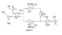
- Figure 2 shows a principal circuit diagram of an embodiment.
- FIG 2 shows an embodiment of the circuit 100, the input connector 105, the first amplifier branch 110, the second amplifier branch 115, and the output connector 120.
- the in- and output connectors 105, 120 can also be referred to as ports.
- the circuit 100 may further comprise a power distribution network 125 for distributing the power of the electrical signal between the first and the second amplifier branches 110, 115 according to a predefmed ratio.
- the predefined ratio may depend on the operating point of the circuit.
- the predefined ratio can be such that the second transistor provides at least 2/3 of a total output power of both transistors when both transistors provide their maximum output power.
- the circuit 100 further comprises an impedance transforming network 125 for changing the phase of the electrical signal such that at an input signal of the first amplifier branch 110 substantially has a phase, which is 90 degrees ahead of an input signal of the second amplifier branch 115.
- the power distribution network and the impedance transforming network are shown as one entity 125. In other embodiments they can be implemented as separate entities.
- the circuit 100 may comprise an impedance transforming network 130 at the output of the first amplifier branch 110.
- the first and the second impedance transforming networks 125 and 130 may be adapted to a Doherty amplifier structure, i.e. the impedance transforming network 125 at the input may change the phase of the input signals to the first and second amplifier branches 110, 115, such that, together with another phase change of the output signals by the impedance transforming network 130, the phase of the output signal of the second amplifier branch 115 is such that an impedance at the output of the first amplifier branch 110 is decreased with increasing output power of the second amplifier branch 115.
- the second amplifier branch can be adapted for amplifying the electrical signal when a level of the electrical signal is above the predefined threshold, and for not amplifying the electrical signal when the level of the electrical signal is below the predefined threshold.
- the impedance transforming network 130 can be adapted to provide a higher output impedance to the first amplifier branch 110, when the level of the electrical signal is below the predefined threshold as compared to when the level of the electrical signal is above the predefined threshold.
- embodiments may further comprise a referencing network 135 to a reference potential.
- Figure 2 can also be interpreted as a principal schematic of an asymmetric Doherty amplifier.
- the power distribution network 125, the impedance transforming network 125, respectively may correspond to an input splitter for splitting the input signal, i.e. the electrical signal, between a main amplifier, corresponding to the first amplifier branch 110, and a peak amplifier, corresponding to the second amplifier branch 115.
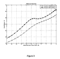
- Figure 3 shows a view chart illustrating efficiency increases with an embodiment.
- the back off from the maximum output power of a Doherty amplifier, along the lines of Figure 2 is shown on the abscissa. The back off is given in dB. The drain efficiency is shown on the ordinate and given in percent.
- Figure 3 shows a comparison of two asymmetric Doherty structures. The first is implemented using LDMOS transistors in both amplifier branches and its results are indicated by circular markers. The second structure uses a hybrid Doherty structure according to an embodiment using two different transistor-technologies for the main and the peak device, i.e. for the first and the second amplifier branches.
- the amplifier concept of the second structure also corresponds to an asymmetric Doherty with a power split ratio of 1:2 between the main, first amplifier branch, and peak amplifier, second amplifier branch.
- the embodiment seeks to improve efficiency at an output back off of -7.8dB. This efficiency maximum is mainly determined by the efficiency of the main transistor, i.e. the first transistor in the first amplifier branch. Therefore this embodiment uses a highly efficient GaN-transistor as main device for the first amplifier branch and a relatively cheap LDMOS-transistor as peak device for the second amplifier branch.
- the word "Hybrid" in this case refers to the two different transistor technologies used.
- the results for the second structure are indicated by square-shaped markers.
- the efficiency of the Hybrid Doherty in the embodiment is significantly higher than that of a LDMOS-only amplifier. Efficiency improvements in the range of 10% can be expected over a large dynamic range.
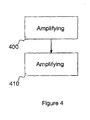
- Embodiments may also provide a radio transmitter comprising an embodiment of the above circuit 100. Moreover, embodiments may provide a method for amplifying an electrical signal, as illustrated by the flow chart in Figure 4 .
- the method may comprise a step 400 of amplifying the electrical signal with a first amplifier branch 110 comprising a first transistor and a step 410 of amplifying the electrical signal with a second amplifier branch 115 comprising a second transistor, when the level of the electrical signal is above a predefined threshold.
- the first and the second transistors are based on different transistor technologies.
- any functional blocks labeled as "power distribution network” may be provided through the use of dedicated hardware, as e.g. an application specific integrated circuit ASIC processor, a controller, as well as hardware capable of executing software in association with appropriate software.
- dedicated hardware e.g. an application specific integrated circuit ASIC processor, a controller
- hardware capable of executing software in association with appropriate software.
- the functions may be provided by a single dedicated processor, by a single shared processor, or by a plurality of individual processors, some of which may be shared.
- processor or “controller” should not be construed to refer exclusively to hardware capable of executing software, and may implicitly include, without limitation, digital signal processor (DSP) hardware, network processor, application specific integrated circuit (ASIC), field programmable gate array (FPGA), read only memory (ROM) for storing software, random access memory (RAM), and non-volatile storage.
- DSP digital signal processor
- ASIC application specific integrated circuit
- FPGA field programmable gate array
- ROM read only memory
- RAM random access memory
- non-volatile storage Other hardware, conventional and/or custom, may also be included.
- any block diagrams herein represent conceptual views of illustrative circuitry embodying the principles of the invention.
- any flow charts, flow diagrams, state transition diagrams, pseudo code, and the like represent various processes which may be substantially represented in computer readable medium and so executed by a computer or processor, whether or not such computer or processor is explicitly shown.
Landscapes
- Engineering & Computer Science (AREA)
- Power Engineering (AREA)
- Amplifiers (AREA)
Priority Applications (1)
| Application Number | Priority Date | Filing Date | Title |
|---|---|---|---|
| EP11290110A EP2495871A1 (de) | 2011-03-03 | 2011-03-03 | Doherty-Verstärker mit unterschiedlichen Transistortechnologien |
Applications Claiming Priority (1)
| Application Number | Priority Date | Filing Date | Title |
|---|---|---|---|
| EP11290110A EP2495871A1 (de) | 2011-03-03 | 2011-03-03 | Doherty-Verstärker mit unterschiedlichen Transistortechnologien |
Publications (1)
| Publication Number | Publication Date |
|---|---|
| EP2495871A1 true EP2495871A1 (de) | 2012-09-05 |
Family
ID=44260055
Family Applications (1)
| Application Number | Title | Priority Date | Filing Date |
|---|---|---|---|
| EP11290110A Withdrawn EP2495871A1 (de) | 2011-03-03 | 2011-03-03 | Doherty-Verstärker mit unterschiedlichen Transistortechnologien |
Country Status (1)
| Country | Link |
|---|---|
| EP (1) | EP2495871A1 (de) |
Cited By (4)
| Publication number | Priority date | Publication date | Assignee | Title |
|---|---|---|---|---|
| CN103326671A (zh) * | 2013-06-25 | 2013-09-25 | 浙江三维无线科技有限公司 | 一种适用于低频段的宽带高效Doherty功放 |
| CN104579186A (zh) * | 2013-10-22 | 2015-04-29 | 北京同方吉兆科技有限公司 | 一种可用于射频功放线性化的模拟预失真放大器 |
| CN104734647A (zh) * | 2013-12-18 | 2015-06-24 | 中兴通讯股份有限公司 | 一种放大器系统及设备 |
| WO2015100489A1 (en) * | 2013-12-31 | 2015-07-09 | Alcatel Lucent | System and method for amplifier design |
Citations (3)
| Publication number | Priority date | Publication date | Assignee | Title |
|---|---|---|---|---|
| US20040222847A1 (en) * | 2003-05-06 | 2004-11-11 | Ahmad Khanifar | RF amplifier employing active load linearization |
| US20090206928A1 (en) * | 2006-09-29 | 2009-08-20 | Nortel Networks Limited | Enhanced doherty amplifier with asymmetrical semiconductors |
| EP2315351A1 (de) * | 2009-10-26 | 2011-04-27 | Alcatel Lucent | Doherty-Leistungsverstärker |
-
2011
- 2011-03-03 EP EP11290110A patent/EP2495871A1/de not_active Withdrawn
Patent Citations (3)
| Publication number | Priority date | Publication date | Assignee | Title |
|---|---|---|---|---|
| US20040222847A1 (en) * | 2003-05-06 | 2004-11-11 | Ahmad Khanifar | RF amplifier employing active load linearization |
| US20090206928A1 (en) * | 2006-09-29 | 2009-08-20 | Nortel Networks Limited | Enhanced doherty amplifier with asymmetrical semiconductors |
| EP2315351A1 (de) * | 2009-10-26 | 2011-04-27 | Alcatel Lucent | Doherty-Leistungsverstärker |
Non-Patent Citations (1)
| Title |
|---|
| DOHERTY, M: "A new high efficiency power amplifier for modulated waves", ANNUAL CONVENTION OF THE INSTITUTE OF RADIO ENGINEERS, 1936 |
Cited By (7)
| Publication number | Priority date | Publication date | Assignee | Title |
|---|---|---|---|---|
| CN103326671A (zh) * | 2013-06-25 | 2013-09-25 | 浙江三维无线科技有限公司 | 一种适用于低频段的宽带高效Doherty功放 |
| CN103326671B (zh) * | 2013-06-25 | 2016-09-28 | 浙江三维无线科技有限公司 | 一种适用于低频段的宽带高效Doherty功放 |
| CN104579186A (zh) * | 2013-10-22 | 2015-04-29 | 北京同方吉兆科技有限公司 | 一种可用于射频功放线性化的模拟预失真放大器 |
| CN104734647A (zh) * | 2013-12-18 | 2015-06-24 | 中兴通讯股份有限公司 | 一种放大器系统及设备 |
| CN104734647B (zh) * | 2013-12-18 | 2018-07-17 | 中兴通讯股份有限公司 | 一种放大器系统及通信设备 |
| WO2015100489A1 (en) * | 2013-12-31 | 2015-07-09 | Alcatel Lucent | System and method for amplifier design |
| US9286429B2 (en) | 2013-12-31 | 2016-03-15 | Alcatel Lucent | System and method for amplifier design |
Similar Documents
| Publication | Publication Date | Title |
|---|---|---|
| US11973468B2 (en) | Apparatus and methods for envelope tracking | |
| US11881818B2 (en) | Envelope tracking for Doherty power amplifiers | |
| KR101145666B1 (ko) | 고주파용 3-스테이지 질화 갈륨계 고전자 이동도 트랜지스터(GaN HEMT) 도허티 전력증폭기 | |
| JP3841416B2 (ja) | 送信装置、送信出力制御方法、および無線通信装置 | |
| CA2234335C (en) | High efficiency power amplifier | |
| CN102549915B (zh) | 多尔蒂放大器 | |
| Bumman et al. | Efficiently amplified | |
| US8098092B2 (en) | Power amplifier | |
| KR101936664B1 (ko) | 전력 증폭기, 무선 원격 유닛 및 기지국 | |
| Son et al. | A highly efficient asymmetric Doherty power amplifier with a new output combining circuit | |
| KR101677555B1 (ko) | 도허티 증폭기에서 낮은 전력 영역에서의 효율을 향상시키기 위한 장치 | |
| CN105981295A (zh) | 具有可调输出功率回退的序贯宽带多尔蒂(Doherty)功率放大器 | |
| CN102282761A (zh) | 高频放大器、无线设备和控制方法 | |
| Bhardwaj et al. | Broadband parallel Doherty power amplifier in GaN for 5G applications | |
| US8395443B2 (en) | Doherty amplifier | |
| Kim et al. | Envelope amplifier with multiple-linear regulator for envelope tracking power amplifier | |
| US11411540B2 (en) | Power amplifier and radio frequency device comprising the same | |
| EP2495871A1 (de) | Doherty-Verstärker mit unterschiedlichen Transistortechnologien | |
| Honda et al. | Efficiency enhancement of GaN Doherty power amplifier at large power back-off with virtual short stub technique | |
| JP2006166141A (ja) | ドハティ増幅器 | |
| Darraji et al. | Generic load-pull-based design methodology for performance optimisation of Doherty amplifiers | |
| EP2536026A1 (de) | Leistungsverstärkerrohr und leistungsverstärkungsverfahren | |
| CN105874705B (zh) | 具有受控包络跟踪调制器和经适配的静态电压的功率放大器设备 | |
| Mimis et al. | A load-modulated low-power amplifier with average power tracking | |
| Lee et al. | A highly efficient three-stage Doherty power amplifier with flat gain for WCDMA applications |
Legal Events
| Date | Code | Title | Description |
|---|---|---|---|
| PUAI | Public reference made under article 153(3) epc to a published international application that has entered the european phase |
Free format text: ORIGINAL CODE: 0009012 |
|
| AK | Designated contracting states |
Kind code of ref document: A1 Designated state(s): AL AT BE BG CH CY CZ DE DK EE ES FI FR GB GR HR HU IE IS IT LI LT LU LV MC MK MT NL NO PL PT RO RS SE SI SK SM TR |
|
| AX | Request for extension of the european patent |
Extension state: BA ME |
|
| 17P | Request for examination filed |
Effective date: 20130305 |
|
| STAA | Information on the status of an ep patent application or granted ep patent |
Free format text: STATUS: THE APPLICATION IS DEEMED TO BE WITHDRAWN |
|
| 18D | Application deemed to be withdrawn |
Effective date: 20130306 |