EP2495988B1 - Procédé et appareil de traitement d'image et d'alimentation de courant - Google Patents
Procédé et appareil de traitement d'image et d'alimentation de courant Download PDFInfo
- Publication number
- EP2495988B1 EP2495988B1 EP11182695.4A EP11182695A EP2495988B1 EP 2495988 B1 EP2495988 B1 EP 2495988B1 EP 11182695 A EP11182695 A EP 11182695A EP 2495988 B1 EP2495988 B1 EP 2495988B1
- Authority
- EP
- European Patent Office
- Prior art keywords
- terminal
- image processing
- processing apparatus
- connector
- circuit
- Prior art date
- Legal status (The legal status is an assumption and is not a legal conclusion. Google has not performed a legal analysis and makes no representation as to the accuracy of the status listed.)
- Active
Links
Images


Classifications
-
- H—ELECTRICITY
- H04—ELECTRIC COMMUNICATION TECHNIQUE
- H04N—PICTORIAL COMMUNICATION, e.g. TELEVISION
- H04N5/00—Details of television systems
- H04N5/44—Receiver circuitry for the reception of television signals according to analogue transmission standards
-
- H—ELECTRICITY
- H04—ELECTRIC COMMUNICATION TECHNIQUE
- H04N—PICTORIAL COMMUNICATION, e.g. TELEVISION
- H04N21/00—Selective content distribution, e.g. interactive television or video on demand [VOD]
- H04N21/40—Client devices specifically adapted for the reception of or interaction with content, e.g. set-top-box [STB]; Operations thereof
- H04N21/43—Processing of content or additional data, e.g. demultiplexing additional data from a digital video stream; Elementary client operations, e.g. monitoring of home network or synchronising decoder's clock; Client middleware
- H04N21/443—OS processes, e.g. booting an STB, implementing a Java virtual machine in an STB or power management in an STB
- H04N21/4436—Power management, e.g. shutting down unused components of the receiver
-
- G—PHYSICS
- G09—EDUCATION; CRYPTOGRAPHY; DISPLAY; ADVERTISING; SEALS
- G09G—ARRANGEMENTS OR CIRCUITS FOR CONTROL OF INDICATING DEVICES USING STATIC MEANS TO PRESENT VARIABLE INFORMATION
- G09G5/00—Control arrangements or circuits for visual indicators common to cathode-ray tube indicators and other visual indicators
- G09G5/003—Details of a display terminal, the details relating to the control arrangement of the display terminal and to the interfaces thereto
- G09G5/006—Details of the interface to the display terminal
-
- H—ELECTRICITY
- H04—ELECTRIC COMMUNICATION TECHNIQUE
- H04N—PICTORIAL COMMUNICATION, e.g. TELEVISION
- H04N21/00—Selective content distribution, e.g. interactive television or video on demand [VOD]
- H04N21/40—Client devices specifically adapted for the reception of or interaction with content, e.g. set-top-box [STB]; Operations thereof
- H04N21/43—Processing of content or additional data, e.g. demultiplexing additional data from a digital video stream; Elementary client operations, e.g. monitoring of home network or synchronising decoder's clock; Client middleware
- H04N21/436—Interfacing a local distribution network, e.g. communicating with another STB or one or more peripheral devices inside the home
- H04N21/43615—Interfacing a Home Network, e.g. for connecting the client to a plurality of peripherals
-
- H—ELECTRICITY
- H04—ELECTRIC COMMUNICATION TECHNIQUE
- H04N—PICTORIAL COMMUNICATION, e.g. TELEVISION
- H04N21/00—Selective content distribution, e.g. interactive television or video on demand [VOD]
- H04N21/40—Client devices specifically adapted for the reception of or interaction with content, e.g. set-top-box [STB]; Operations thereof
- H04N21/43—Processing of content or additional data, e.g. demultiplexing additional data from a digital video stream; Elementary client operations, e.g. monitoring of home network or synchronising decoder's clock; Client middleware
- H04N21/436—Interfacing a local distribution network, e.g. communicating with another STB or one or more peripheral devices inside the home
- H04N21/4363—Adapting the video stream to a specific local network, e.g. a Bluetooth® network
- H04N21/43632—Adapting the video stream to a specific local network, e.g. a Bluetooth® network involving a wired protocol, e.g. IEEE 1394
- H04N21/43635—HDMI
-
- H—ELECTRICITY
- H04—ELECTRIC COMMUNICATION TECHNIQUE
- H04N—PICTORIAL COMMUNICATION, e.g. TELEVISION
- H04N5/00—Details of television systems
- H04N5/63—Generation or supply of power specially adapted for television receivers
-
- G—PHYSICS
- G09—EDUCATION; CRYPTOGRAPHY; DISPLAY; ADVERTISING; SEALS
- G09G—ARRANGEMENTS OR CIRCUITS FOR CONTROL OF INDICATING DEVICES USING STATIC MEANS TO PRESENT VARIABLE INFORMATION
- G09G2330/00—Aspects of power supply; Aspects of display protection and defect management
- G09G2330/02—Details of power systems and of start or stop of display operation
-
- G—PHYSICS
- G09—EDUCATION; CRYPTOGRAPHY; DISPLAY; ADVERTISING; SEALS
- G09G—ARRANGEMENTS OR CIRCUITS FOR CONTROL OF INDICATING DEVICES USING STATIC MEANS TO PRESENT VARIABLE INFORMATION
- G09G2370/00—Aspects of data communication
- G09G2370/04—Exchange of auxiliary data, i.e. other than image data, between monitor and graphics controller
-
- G—PHYSICS
- G09—EDUCATION; CRYPTOGRAPHY; DISPLAY; ADVERTISING; SEALS
- G09G—ARRANGEMENTS OR CIRCUITS FOR CONTROL OF INDICATING DEVICES USING STATIC MEANS TO PRESENT VARIABLE INFORMATION
- G09G2370/00—Aspects of data communication
- G09G2370/12—Use of DVI or HDMI protocol in interfaces along the display data pipeline
-
- G—PHYSICS
- G09—EDUCATION; CRYPTOGRAPHY; DISPLAY; ADVERTISING; SEALS
- G09G—ARRANGEMENTS OR CIRCUITS FOR CONTROL OF INDICATING DEVICES USING STATIC MEANS TO PRESENT VARIABLE INFORMATION
- G09G2370/00—Aspects of data communication
- G09G2370/22—Detection of presence or absence of input display information or of connection or disconnection of a corresponding information source
-
- G—PHYSICS
- G09—EDUCATION; CRYPTOGRAPHY; DISPLAY; ADVERTISING; SEALS
- G09G—ARRANGEMENTS OR CIRCUITS FOR CONTROL OF INDICATING DEVICES USING STATIC MEANS TO PRESENT VARIABLE INFORMATION
- G09G5/00—Control arrangements or circuits for visual indicators common to cathode-ray tube indicators and other visual indicators
- G09G5/003—Details of a display terminal, the details relating to the control arrangement of the display terminal and to the interfaces thereto
Definitions
- Methods and apparatuses consistent with the exemplary embodiments relate to an image processing apparatus, to which an external device is communicatively connected, e.g. depending on preset standards, and a control method thereof. More particularly, the exemplary embodiments are preferably directed to an image processing apparatus having a structure where charge power can be supplied to an external device through a cable connected to the corresponding external device, and a control method thereof.
- An image processing apparatus processes video contents received from a exterior device through various processes, and either displays the processed video contents on its own display panel or outputs the processed video to another image processing apparatus to be displayed as an image on the corresponding image processing apparatus.
- the image processing apparatus may include a television or a monitor in the situation of having its own display panel, or may include a digital versatile disc (DVD)/Blu-ray disc (BD), a set top box, etc. in the situation of having no display panel.
- an image processing system having plural image processing apparatuses communicatively connected each other, by a wire or wirelessly, is often used, rather than using an image processing apparatus independently.
- an image processing apparatus there is a system where a DVD/BD player and a TV are connected by a cable complying with preset standards, , and an image reproduced by the DVD/BD player is displayed on the TV.
- power or a control signal for operational control as well as a video signal containing video contents may be transmitted and received between an image processing apparatus and another image processing apparatus, which are connected to each other.
- a cable and a connector of the image processing apparatus, to which the cable is connected have a plurality of corresponding pins or terminals, in order that the cable and the connector can be physically connected to each other, thereby transmitting various characteristic signals through the plurality of pins or terminals.
- Document EP2172831A1 discloses a transmission device, power supply and switching method.
- the switching unit may include a detection circuit which detects whether the second terminal and the third terminal are connected; and a first switching circuit which is turned on to supply power from the image processing apparatus to the first terminal in response to a detection by the detection circuit that the second terminal and the third terminal are connected.
- the detection circuit may include a pull-up circuit connected to the third terminal.
- the first switching circuit may be connected to the second terminal and turned on by the pull-up circuit so that power from the image processing apparatus can be transmitted to the first terminal when the second terminal and the third terminal are connected.
- the pull-up circuit may include a resistor connected to power and the third terminal.
- the detection circuit may include a pull-down circuit connected to the second terminal and the first switching circuit.
- the first switching circuit may be turned off by the pull-down circuit so that the power of the image processing apparatus cannot be transmitted to the first terminal when the second terminal and the third terminal are disconnected.
- the pull-down circuit may include a resistor connected to ground.
- the switching unit may include a second switching circuit for connecting the chipset unit to the first terminal and the first switching circuit.
- the second switching circuit may be turned on or off by the pull-up circuit and the pull-down circuit in a reverse manner as with the first switching circuit.
- the second switching circuit may prevent the power of the image processing apparatus supplied to the first terminal from being supplied to the chipset unit when the first switching circuit is turned on.
- the second switching circuit may allow the first terminal and the chipset unit to be connected when the first switching circuit is turned off.
- the switching unit may include a controller which turns on the first switching circuit and turns off the second switching circuit in response to connection to the pull-up circuit.
- the controller may turn off the first switching circuit and turn on the second switching circuit in response to being disconnected from the pull-up circuit.
- the switching unit may shut off the power from the image processing apparatus to the first terminal in response to the cable connected to the connector complying with a second preset standard not to connect the second terminal and the third terminal, or in response to the cable not being connected to the connector.
- Another aspect may be achieved by providing a control method of an image processing apparatus according to claim 12 herein.
- the switching may include detecting whether the second terminal and the third terminal are connected; allowing the power from the image processing apparatus to be supplied to the first terminal in response to a detection that the second terminal and the third terminal are connected; and shutting off the power from the image processing apparatus to the first terminal in response to a detection that the second terminal and the third terminal are disconnected.
- the allowing the power of the image processing apparatus to be supplied to the first terminal in response to a detection that the second terminal and the third terminal are connected may include preventing the power from the image processing apparatus, supplied to the first terminal, from being supplied to the chipset unit.
- the shutting off of the power from the image processing apparatus to the first terminal in response to a detection that the second terminal and the third terminal are disconnected, may include allowing the first terminal and the chipset unit to be connected.
- the switching may include shutting off the power from the image processing apparatus to the first terminal in response to the cable connected to the connector complying with a second preset standard not to connect the second terminal and the third terminal, or in response to the cable not being connected to the connector.
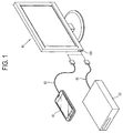
- FIG. 1 illustrates an external device 30 connected to an image processing apparatus 10 according to a first exemplary embodiment.
- image processing apparatus 10 and external devices 20 and 30 are connected for interactive communication through cables 40 and 50.
- image processing apparatus 10 includes at least one connector 100 to which cables 40 and 50 are physically connected.
- image processing apparatus 10 includes one connector 100, but not limited thereto.
- the image processing apparatus may include a plurality of connectors 100, and each connector 100 may correspond to one connector 100 described in this exemplary embodiment.
- image processing apparatus 10 is a display apparatus capable of displaying an image
- external devices 20 and 30 are a DVD/BD player 20 or a mobile device 30, but not limited thereto.
- the above examples do not limit the inventive concept.
- Image processing apparatus 10 can be connected to one of external devices 20 and 30 through connector 100 and cables 40 and 50 connected to connector 100. Image processing apparatus 10 can interactively communicate with external devices 20 and 30. Further, various characteristic signals, such as, a video signal containing video contents, a control signal for operation control of the image processing apparatus 10 or external devices 20 and 30, or unlimited various kinds of data, power, etc. may be transmitted and received between image processing apparatus 10 and external devices 20 and 30.
- connector 100 of image processing apparatus 10 complies with high definition multimedia interface (HDMI) standards.
- HDMI high definition multimedia interface
- Connector 100 in accordance with HDMI standards, includes 19 pins/terminals for transmitting a signal.
- a first cable 40 connected to first device 20 complies with the HDMI standards, like connector 100.
- a second cable 50 connected to second device 30 complies with mobile high-definition link (MHL) standards.
- MHL mobile high-definition link
- the MHL standard is a modified protocol of the HDMI standard for connecting a relatively small mobile device 30 with image processing apparatus 10.
- Second cable 50 of the MHL standards is connectable with connector 100 of the HDMI standards.
- Second cable 50 uses 6 terminals from among the 19 terminals of connector 100.
- Cable 50 of the MHL standards is different from cable 40 of the HDML standards in characteristics or transmissive direction of a signal transmitted through these 6 terminals. In the situation where cables 40 and 50 are connected to connector 100, an example where a signal is assigned to each terminal of connector 100 in accordance with respective standards, will be described later.
- the HDMI and MHL standards and the number of terminals provided in connector 100 are specifically described, but not limited thereto. That is, the present inventive concept may be applied to the HDMI and MHL standards with the exception that the standards specifically illustrated in this exemplary embodiment, and may not be restricted by the number and configurations of terminals provided in the connector 100, signal assignment of each terminal, etc.
- FIG. 2 is a block diagram of the image processing apparatus of FIG. 1 .
- image processing apparatus 10 includes a connector 100 to which a first cable 40 connecting with a first device 20 or a second cable 50 connecting with a second device 30 is connected.
- Image processing apparatus 10 further includes chipset unit 200 which processes data on the basis of a preset process, and a power supply 300 which supplies operation power to different elements.
- connector 100 complies with the HDMI standards, and allows one of the external devices 20 and 30 to interactively communicate with chipset unit 200. Detailed configurations of connector 100 will be described later.
- Chipset unit 200 is achieved by a system-on-chip (SOC) or a combination group of various chipsets, and performs various processes related to image processing.
- Chipset unit 200 may transmit and receive data/control signal/power/etc. to and from external device 20, 30 connected through connector 100, as well as perform the image processing, and processes the corresponding data/control signal/power on the basis of the preset process.
- SOC system-on-chip
- Chipset unit 200 may transmit and receive data/control signal/power/etc. to and from external device 20, 30 connected through connector 100, as well as perform the image processing, and processes the corresponding data/control signal/power on the basis of the preset process.
- Power supply 300 converts alternating current (AC) power received from the exterior of image processing apparatus 10 into direct current (DC) power of various levels, and supplies them to the respective elements of image processing apparatus 10.
- power supply 300 may receive DC power from a battery (not shown) and supply power to image processing apparatus 10.
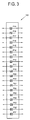
- connector 100 has 19 terminals based on the HDMI standards, as shown in FIG. 3.
- FIG. 3 shows the respective terminals of the connector 100.
- connector 100 includes total 19 terminals from P01 to P19. If first cable 40, complying with the HDMI standards, is connected to connector 100, 19 terminals of connector 100 are connected, respectively, to 19 terminals of first cable 40.
- TMDS transition minimized differential signaling
- CED consumer electronics control
- DDC display data channel
- second cable 50 complying with the MHL standards
- 6 terminals (P02, P10, P12, P15, P18 and P19) of the among 19 terminals (P01 to P19) of connector 100 are connected to second cable 50.
- the characteristics of the signals assigned to the respective terminals (P01 to P19) of connector 100, as shown in the table 1 are changed.
- a signal where data and clocks are combined is transmitted and received through terminals P10 and P12; terminal P18 forms a power bus, and terminal P19 forms a control bus.
- chipset unit 200 of image processing apparatus 10 is configured to supply charging power to second device 30 when receiving a preset control signal from second device 30.
- the second device 30 has to transmit the control signal to image processing apparatus 10. Therefore, power remaining in the battery (not shown) of second device 30 has to be sufficient enough to transmit the control signal. That is, with the above configuration, in response to the power remaining in the battery (not shown) of second device 30 being zero, it is difficult for image processing apparatus 10 to supply the charging power to second device 30.
- chipset unit 200 controls the power to be supplied from power supply 300 to second device 30.
- chipset unit 200 enters a standby mode in a standby mode of image processing apparatus 10. Accordingly, it is difficult to supply power to the second device. That is, in response to image processing apparatus 10 not being a normal mode but rather being in the standby mode, it is difficult to supply charging power to second device 30.
- image processing apparatus 10 in this exemplary embodiment includes a switching unit 400, as shown in FIG. 2 .
- switching unit 400 can supply the power of image processing apparatus 10 to external device 30 via the first terminal, and selectively switches the supply of power to the first terminal on the basis of a signal state of the second terminal, when cable 40, 50 is connected to connector 100.
- the signal state of the second terminal is, for example, changed between high and low (or between 0 and 1) in accordance with whether or not the third terminal of connector 100 is connected to the second terminal.
- switching unit 400 can detect whether second cable 50 complying with the MHL standards, is connected to connector 100. In response to a detection that second cable 50, complying with the MHL standards, is connected, switching unit 400 allows the power of image processing apparatus 10 to be supplied to the first terminal.
- image processing apparatus 10 can supply the charge power to second device 30 via second cable 50 even though the power remaining in the battery (not shown) of second device 30 is zero or image processing apparatus 10 is in the standby mode.
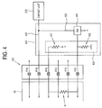
- FIG. 4 is a circuit diagram of the connector and a switching unit in the image processing apparatus of FIG. 1 .
- FIG. 4 only minimum configurations directly related to the present inventive concept will be described and illustrated.
- terminals P02, P10, P12, P15, P18 and P19 from among the 19 terminals of connector 100, comply with the MHL standards.
- terminal P18 is connected to chipset unit 200 via a first line 410, and a second line 420 is connected to the power of the image processing apparatus 10, e.g., standby power of +5V is branched from first line 410.
- Switching unit 400 includes a detection circuit 430 for detecting a connection between the terminals P02 and P15, and a switching circuit 440, which is turned on in order to supply the power of image processing apparatus 10 to terminal P18 in response to a detection by detection circuit 430 that terminals P02 and P15 are connected.
- Detection circuit 430 includes a pull-up circuit 431 connected to the terminal P15, and a pull-down circuit 432 connected to terminal P02.
- Pull-up circuit 431 and pull-down circuit 432 are configured, respectively, to include resistors having predetermined resistance.
- Pull-up circuit 431 connects to the power of +5V, as the standby power for image processing apparatus 10, and pull-down circuit 432 connects to ground.
- Switching circuit 440 is installed on second line 420, and connects with terminal P02 and pull-down circuit 432.
- Switching circuit 440 is configured to include a transistor (not shown) to which the power of image processing apparatus 10 is connected.
- switching circuit 440 is turned off by pull-down circuit 432.
- second line 420 becomes open and the power passing through second line 420 is shut off.
- second cable 50 complying with the MHL standards is configured to include lines, respectively which correspond to terminals P02 and P15 of connector 100, which are connected to each other through a resistor 51 having predetermined resistance, e.g., 3.3k ⁇ .
- terminals P02 and P15 are connected to each other and the pull-up circuit 431 is connected to switching circuit 440.
- the connection is via the terminal P15, the second cable 50 and the terminal P02.
- pull-up circuit 431 causes the signal state of terminal P02 to become high, by way of example, between high and low.
- the high/low states are provided just to distinguish the signal states from one another.
- switching circuit 440 is turned on by pull-up circuit 431, and therefore second line 420 becomes closed and the power is supplied to first line 410 and terminal P18.
- This supplied power for charging is supplied from terminal P18 to second device 30 via the second cable 50.
- switching unit 400 can selectively supply power to terminal P18 in accordance with second cable 50 complying with the MHL standards.
- image processing apparatus 10 can supply power to second device 30.
- switching circuit 440 is turned off by pull-down circuit 432, and shuts off the power supplied through second line 420.
- second line 420 is switched to become open/closed in accordance with the standards of whichever cable 40, 50 is connected to connector 100.
- the apparatus may be configured to prevent the power supplied to terminal P18 from being supplied to chipset unit 200 when second cable 50 is connected to connector 100.
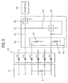
- FIG. 5 is a schematic circuit diagram of connector 100 and switching unit 500 in an image processing apparatus according to a second exemplary embodiment.
- a first line 510 connects the chipset unit 200 and the terminal P18.
- a second line 520, to which power is supplied, is branched from a node 511 of first line 510.
- Switching unit 500 includes a detection circuit 530 for detecting a connection between terminals P02 and P15, a first switching circuit 540 installed on second line 520 and switching second line 520 to be opened and closed.
- a second switching circuit 550 is installed on first line 510 between node 511 and chipset unit 200 of first line 510 and switches first line 510 open and closed.
- Detection circuit 530 includes a pull-up circuit 531 connected to terminal P15, and a pull-down circuit 532 connected to terminal P02.
- Detection circuit 530 and first switching circuit 540 correspond to detection circuit 430 and switching circuit 440 (refer to FIG. 4 ) described in the foregoing first exemplary embodiment. Thus, repetitive descriptions thereof will be avoided.
- Second switching circuit 550 switches connection of the chipset unit 200 to terminal P18 and switching circuit 540.
- Second switching circuit 550 is achieved by a transistor such as the transistor in first switching circuit 540, and is switched to be turned on/off by detection circuit 530.
- Second switching circuit 550 is turned on/off in reverse to first switching circuit 540, under operation of detection circuit 530, i.e., the pull-up circuit 531 and pull-down circuit 532.
- pull-up circuit 531 turns on first switching circuit 540 and turns off second switching circuit 550. That is, since first switching circuit 540 is turned off, the power supplied through second line 520 is shut off. However, the connection between terminal P18 and chipset unit 200 is permitted. In response to first cable 40 being connected to connector 100, chipset unit 200 may receive power from first device 20, via the terminal P18.
- the power supply through terminal P18 and the connection of chipset unit 200 to terminal P18 can be switched in accordance with whether or not cable 50, complying with the MHL standards, is connected to connector 100.
- FIG. 6 is a circuit diagram of a connector 100 and a switching unit 600 in an image processing apparatus according to the third exemplary embodiment.
- a first line 610 connects chipset unit 200 and terminal P18, and a second line 620, to which power is supplied, is branched from a node 611 of first line 610.
- Switching unit 600 includes a detection circuit 630, a first switching circuit 640 and a second switching circuit 650.
- Detection circuit 630 includes a pull-up circuit 631 connected to the terminal P15, and a pull-down circuit 632 connected to terminal P02, which correspond to those of the second exemplary embodiment. Thus, repetitive descriptions thereof will be avoided.
- First switching circuit 640 switches second line 620 to be opened and closed, and second switching circuit 650 switches first line 610 between node 611 and chipset unit 200 to be opened and closed.
- switching unit 600 in this exemplary embodiment includes controller 660 for selectively controlling switching operations of first switching circuit 640 and second switching circuit 650 in accordance with detection results of detection circuit 630.
- Controller 660 is connected to terminal P02 and pull-down circuit 632.
- controller 660 may be achieved by a micro controller unit (MCU), and first switching circuit 640 and second switching circuit 650 may be achieved by a transistor, a relay, etc., but are not limited thereto.
- MCU micro controller unit
- first switching circuit 640 and second switching circuit 650 may be achieved by a transistor, a relay, etc., but are not limited thereto.
- pull-up circuit 631 for example applies a high signal to controller 660.
- controller 660 turns on first switching circuit 640 and turns off second switching circuit 650.
- controller 660 turns off first switching circuit 640 and turns on second switching circuit 650.
- first switching circuit 640 and second switching circuit 650 With regard to whether to supply power, connection states between the elements, etc., depending on the turned-on/off states of first switching circuit 640 and second switching circuit 650, the foregoing exemplary embodiments may be applied thereto and thus repetitive descriptions thereof will be avoided.
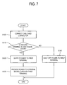
- FIG. 7 is a flowchart showing this operation.
- Connector 100 in this exemplary embodiment includes a first terminal capable of supplying power to external device 30, and second and third terminals for detecting a change in a signal state, depending on connection of the cable 40, 50.
- image forming apparatus 10 determines whether the second terminal is in a high signal state (S110).
- image processing apparatus 10 allows its own power to be supplied to first terminal (S120), and thus provides the power to external device 30 through first terminal (S130).
- image processing apparatus 10 shuts off its own power to first terminal (S140).
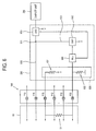
- FIG. 8 is a flowchart showing this operation.
- Connector 100 in this exemplary embodiment includes a first terminal capable of supplying power to external device 30, and second and third terminals for detecting change in a signal state depending on connection of cable 40, 50.
- image forming apparatus 10 determines whether or not the second terminal is in a high signal state (S210).
- image processing apparatus 10 allows its own power to be supplied to first terminal and shuts off the power to chipset unit 200 (S220). Further, image processing apparatus 10 provides power to external device 30 through first terminal (S230).
- image processing apparatus 10 shuts off its own power to the first terminal (S240) and allows a connection between the first terminal and chipset unit 200 (S250).
Landscapes
- Engineering & Computer Science (AREA)
- Multimedia (AREA)
- Signal Processing (AREA)
- Physics & Mathematics (AREA)
- Computer Hardware Design (AREA)
- General Physics & Mathematics (AREA)
- Theoretical Computer Science (AREA)
- General Engineering & Computer Science (AREA)
- Software Systems (AREA)
- Computer Networks & Wireless Communication (AREA)
- Two-Way Televisions, Distribution Of Moving Picture Or The Like (AREA)
- Power Sources (AREA)
Claims (13)
- Dispositif de traitement d'image comprenant :une unité de jeu de puces (200) agencée pour traiter des données ;un connecteur (100) conforme aux normes d'interface multimédia haute définition (HDMI) qui comprend une pluralité de bornes comprenant une première borne, une deuxième borne qui est la borne 2 de blindage de données TDMS du connecteur, et une troisième borne qui est la borne d'horloge DDC du connecteur, le connecteur étant agencé de manière à se connecter à un câble afin que l'unité de jeu de puces puisse émettre et recevoir un signal vers et depuis un dispositif externe ;un bloc d'alimentation (300) agencé pour alimenter l'unité de jeu de puces et une unité de commutation ; etl'unité de commutation (400) agencée de manière à fournir de l'énergie du dispositif de traitement d'image au dispositif externe par l'intermédiaire de ladite première borne, et à commander sélectivement une opération de commutation s'il faut ou non fournir de l'énergie du dispositif de traitement d'image à la première borne sur la base d'un état de signal de ladite deuxième borne quand le câble est connecté au connecteur ;dans lequel ladite troisième borne reçoit une tension du dispositif de traitement d'image ;ce par quoi ledit état de signal est un premier état de signal de tension quand le câble connecté au connecteur est conforme aux normes HDMI de façon que la deuxième borne ne soit ainsi pas connectée à la troisième borne, et ledit état de signal est un deuxième état de signal de tension quand le câble connecté au connecteur est conforme aux normes de lien haute définition mobile (MHL) de façon que la deuxième borne soit ainsi connectée à la troisième borne et à ladite tension fournie de celle-ci ; etdans lequel l'unité de commutation est agencée de manière à détecter ledit deuxième état de signal de tension de ladite deuxième borne tandis que l'unité de jeu de puces est dans un mode veille et, si cela est détecté, à fournir de l'énergie du dispositif de traitement d'image à la première borne.
- Dispositif de traitement d'image selon la revendication 1, dans lequel le premier état de signal de tension comprend un état de signal de tension basse et le deuxième état de signal de tension comprend un état de signal de tension haute.
- Dispositif de traitement d'image selon la revendication 2, dans lequel l'unité de commutation comprend
un circuit de détection qui détecte si la deuxième borne et la troisième borne sont connectées ; et
un premier circuit de commutation qui est mis en service pour fournir de l'énergie du dispositif de traitement d'image à la première borne en réponse à une détection par le circuit de détection détecte que la deuxième borne et la troisième borne sont connectées. - Dispositif de traitement d'image selon la revendication 3, dans lequel
le circuit de détection comprend un circuit de rappel au niveau haut connecté à la troisième borne, et
le premier circuit de commutation est connecté à la deuxième borne et mis en service par le circuit de rappel au niveau haut de façon que de l'énergie du dispositif de traitement d'image puisse être transmise à la première borne quand la deuxième borne et la troisième borne sont connectées. - Dispositif de traitement d'image selon la revendication 4, dans lequel le circuit de rappel au niveau haut comprend une résistance connectée au bloc d'alimentation et à la troisième borne.
- Dispositif de traitement d'image selon la revendication 4, dans lequel
le circuit de détection comprend un circuit de rappel au niveau bas connecté à la deuxième borne et au premier circuit de commutation, et
le premier circuit de commutation est mis hors service par le circuit de rappel au niveau bas de façon que l'énergie du dispositif de traitement d'image ne puisse pas être transmise à la première borne quand la deuxième borne et la troisième borne sont déconnectées. - Dispositif de traitement d'image selon la revendication 6, dans lequel le circuit de rappel au niveau bas comprend une résistance connectée à la terre.
- Dispositif de traitement d'image selon la revendication 6, dans lequel l'unité de commutation comprend un deuxième circuit de commutation pour commuter la connexion de l'unité de jeu de puces à la première borne et au premier circuit de commutation.
- Dispositif de traitement d'image selon la revendication 8, dans lequel le deuxième circuit de commutation est mis en service ou hors service par le circuit de rappel au niveau haut et le circuit de rappel au niveau bas à l'inverse du premier circuit de commutation.
- Dispositif de traitement d'image selon la revendication 8, dans lequel le deuxième circuit de commutation empêche l'énergie du dispositif de traitement d'image fournie à la première borne d'être fournie à l'unité de jeu de puces quand le premier circuit de commutation est mis en service, et permet à la première borne et à l'unité de jeu de puces d'être connectées quand le premier circuit de commutation est mis hors service.
- Dispositif de traitement d'image selon la revendication 8, dans lequel l'unité de commutation comprend un contrôleur qui met en service le premier circuit de commutation et met hors service le deuxième circuit de commutation en réponse à une connexion au circuit de rappel au niveau haut, et met hors service le premier circuit de commutation et met en service le deuxième circuit de commutation en réponse à une déconnexion d'avec le circuit de rappel au niveau haut.
- Procédé de commande d'un dispositif de traitement d'image comprenant une unité de jeu de puces qui traite des données ; et un connecteur conforme aux normes d'interface multimédia haute définition (HDMI) qui comprend une pluralité de bornes comprenant une première borne, une deuxième borne qui est la borne 2 de blindage de données TDMS du connecteur, et une troisième borne qui est la borne d'horloge DDC du connecteur, le connecteur étant agencé de manière à se connecter à un câble afin que l'unité de jeu de puces puisse émettre et recevoir un signal vers et depuis un dispositif externe, le procédé comprenant :la commutation sélective (S110) s'il faut ou non fournir de l'énergie du dispositif de traitement d'image à ladite première borne sur la base d'un état de signal de ladite deuxième borne quand le câble est connecté au connecteur ; etla transmission de l'énergie (S120) du dispositif de traitement d'image à la première borne en réponse à l'état de signal de la deuxième borne qui est un deuxième état de signal de tension ;lequel procédé comprend le fait de fournir à ladite troisième borne une tension du dispositif de traitement d'image, ce par quoi ledit état de signal est un premier état de signal de tension quand le câble connecté au connecteur est conforme aux normes HDMI de façon que la deuxième borne ne soit ainsi pas connectée à la troisième borne, et ledit état de signal est ledit deuxième état de signal de tension quand le câble connecté au connecteur est conforme aux normes de lien haute définition mobile (MHL) de façon que la deuxième borne soit ainsi connectée à la troisième borne et à ladite tension fournie de celle-ci, l'état de signal de la deuxième borne variant ainsi en fonction de la connexion d'une troisième borne du connecteur à la deuxième borne ; etla fourniture d'énergie du dispositif de traitement d'image à la première borne si ledit deuxième état de signal de tension de ladite deuxième borne est détecté tandis que l'unité de jeu de puces est dans un mode veille.
- Procédé selon la revendication 12, dans lequel le premier état de signal de tension comprend un état de signal de tension basse et le deuxième état de signal de tension comprend un état de signal de tension haute.
Priority Applications (1)
| Application Number | Priority Date | Filing Date | Title |
|---|---|---|---|
| EP16172970.2A EP3082343A1 (fr) | 2011-03-02 | 2011-09-26 | Procede et appareil de traitement d'image |
Applications Claiming Priority (1)
| Application Number | Priority Date | Filing Date | Title |
|---|---|---|---|
| KR1020110018385A KR101566174B1 (ko) | 2011-03-02 | 2011-03-02 | 영상처리장치 및 그 제어방법 |
Related Child Applications (1)
| Application Number | Title | Priority Date | Filing Date |
|---|---|---|---|
| EP16172970.2A Division EP3082343A1 (fr) | 2011-03-02 | 2011-09-26 | Procede et appareil de traitement d'image |
Publications (2)
| Publication Number | Publication Date |
|---|---|
| EP2495988A1 EP2495988A1 (fr) | 2012-09-05 |
| EP2495988B1 true EP2495988B1 (fr) | 2016-06-08 |
Family
ID=45491229
Family Applications (2)
| Application Number | Title | Priority Date | Filing Date |
|---|---|---|---|
| EP16172970.2A Withdrawn EP3082343A1 (fr) | 2011-03-02 | 2011-09-26 | Procede et appareil de traitement d'image |
| EP11182695.4A Active EP2495988B1 (fr) | 2011-03-02 | 2011-09-26 | Procédé et appareil de traitement d'image et d'alimentation de courant |
Family Applications Before (1)
| Application Number | Title | Priority Date | Filing Date |
|---|---|---|---|
| EP16172970.2A Withdrawn EP3082343A1 (fr) | 2011-03-02 | 2011-09-26 | Procede et appareil de traitement d'image |
Country Status (4)
| Country | Link |
|---|---|
| US (3) | US8930730B2 (fr) |
| EP (2) | EP3082343A1 (fr) |
| KR (1) | KR101566174B1 (fr) |
| CN (2) | CN102655580B (fr) |
Families Citing this family (22)
| Publication number | Priority date | Publication date | Assignee | Title |
|---|---|---|---|---|
| JP2012174203A (ja) * | 2011-02-24 | 2012-09-10 | Sony Corp | ディスプレイ装置、ディスプレイ装置に接続されたブランチ機器の電源供給要否判定方法 |
| KR101566174B1 (ko) | 2011-03-02 | 2015-11-05 | 삼성전자 주식회사 | 영상처리장치 및 그 제어방법 |
| US20130103962A1 (en) * | 2011-10-25 | 2013-04-25 | Handong Lnc Co., Ltd. | Sleep state synchronization method between docked terminals and docking system using the same |
| JP2013254044A (ja) * | 2012-06-06 | 2013-12-19 | Funai Electric Co Ltd | 端末装置、表示装置および表示システム |
| JP6237637B2 (ja) * | 2012-10-16 | 2017-11-29 | ソニー株式会社 | 電子機器、電子機器の充電制御方法、電子機器のバッテリ残量表示方法、ソース機器およびシンク機器 |
| CN102946556B (zh) * | 2012-10-31 | 2015-11-25 | 京东方科技集团股份有限公司 | 一种显示设备以及包括该显示设备的家庭网络系统 |
| KR102005390B1 (ko) * | 2012-10-31 | 2019-07-30 | 엘지디스플레이 주식회사 | 리셋제어부를 포함하는 표시장치 및 그 구동방법 |
| CN102932620B (zh) * | 2012-11-12 | 2016-12-21 | 深圳创维-Rgb电子有限公司 | 电视机及其自动识别mhl信号的方法 |
| JP5777727B2 (ja) * | 2013-06-28 | 2015-09-09 | 株式会社東芝 | テレビジョン装置、リモートコントローラ及び操作信号指示装置 |
| US8959257B2 (en) * | 2013-07-09 | 2015-02-17 | Kabushiki Kaisha Toshiba | Information processing apparatus and information processing method |
| US20150029398A1 (en) * | 2013-07-24 | 2015-01-29 | Kabushiki Kaisha Toshiba | Information processing apparatus and information processing method for outputting a charging status |
| CN103491412B (zh) * | 2013-09-27 | 2016-08-17 | 广州视源电子科技股份有限公司 | 带待机充电功能的mhl设备识别电路 |
| KR102146733B1 (ko) * | 2013-10-31 | 2020-08-24 | 엘지전자 주식회사 | 전자기기 및 그를 포함하는 방송신호 수신기 |
| WO2015101397A1 (fr) * | 2013-12-30 | 2015-07-09 | Arcelik Anonim Sirketi | Gestion d'alimentation de secours dans un dispositif d'affichage d'images avec fonction de réveil par réseau local |
| WO2015183252A1 (fr) * | 2014-05-28 | 2015-12-03 | Hewlett Packard Development Company, L.P. | Circuit |
| TW201630279A (zh) | 2014-09-19 | 2016-08-16 | 鴻慶鑫電聲科技有限公司 | 電連接器、具有該電連接器之連接裝置及連接組合 |
| CN105676986B (zh) * | 2014-11-20 | 2019-01-22 | 鸿富锦精密工业(武汉)有限公司 | 电子设备接口切换系统 |
| WO2016153249A1 (fr) * | 2015-03-23 | 2016-09-29 | 엘지전자(주) | Procédé et dispositif d'émission/réception de puissance au moyen d'une interface hdmi |
| KR102707430B1 (ko) * | 2017-01-25 | 2024-09-20 | 삼성전자주식회사 | 전력 공급 장치 및 그 전력 공급 장치를 포함하는 전력 공급 시스템 |
| KR20200127415A (ko) * | 2019-05-02 | 2020-11-11 | 엘지전자 주식회사 | 디스플레이 장치 |
| JP2021092861A (ja) * | 2019-12-06 | 2021-06-17 | 東芝テック株式会社 | 電子機器 |
| WO2021261715A1 (fr) * | 2020-06-26 | 2021-12-30 | 삼성전자주식회사 | Dispositif récepteur, dispositif source, et leurs procédés de commande |
Citations (4)
| Publication number | Priority date | Publication date | Assignee | Title |
|---|---|---|---|---|
| US20080313477A1 (en) * | 2004-08-11 | 2008-12-18 | Kabushiki Kaisha Toshiba | Information processing apparatus and method for controlling power supply of the apparatus |
| WO2012003328A2 (fr) * | 2010-06-30 | 2012-01-05 | Silicon Image, Inc. | Détection de connexions de câble pour dispositifs électroniques |
| EP2405654A1 (fr) * | 2010-02-12 | 2012-01-11 | Sony Corporation | Appareil électronique et procédé pour la détermination de l'interface numérique d'un dispositif de connexion externe |
| EP2521953A1 (fr) * | 2010-01-06 | 2012-11-14 | Apple Inc. | Alimentation d'un accessoire pendant la veille prolongée d'un dispositif informatique portable |
Family Cites Families (20)
| Publication number | Priority date | Publication date | Assignee | Title |
|---|---|---|---|---|
| JP3263675B2 (ja) * | 1999-02-02 | 2002-03-04 | 三洋電機株式会社 | 共通コネクターを具えた電子機器 |
| JP3558059B2 (ja) | 2001-08-10 | 2004-08-25 | セイコーエプソン株式会社 | 電源制御回路及び電子機器 |
| KR100690581B1 (ko) | 2005-06-29 | 2007-03-09 | 삼성전자주식회사 | 디스플레이장치 |
| US7624202B2 (en) * | 2006-08-17 | 2009-11-24 | Standard Microsystems Corporation | System and method for enumerating a USB device using low power |
| US8272023B2 (en) | 2006-11-02 | 2012-09-18 | Redmere Technology Ltd. | Startup circuit and high speed cable using the same |
| US7996584B2 (en) | 2006-11-02 | 2011-08-09 | Redmere Technology Ltd. | Programmable cable with deskew and performance analysis circuits |
| CN101542992A (zh) * | 2006-11-02 | 2009-09-23 | 雷德米尔技术有限公司 | 具有嵌入式功率控制的一种可编程高速缆线 |
| JP5292776B2 (ja) | 2007-07-19 | 2013-09-18 | ソニー株式会社 | 送信装置、送信装置の電源切換方法、受信装置および受信装置の電源供給方法 |
| DE202007018449U1 (de) | 2007-11-02 | 2008-10-02 | Fujitsu Siemens Computers Gmbh | Elektronisches Gerät, Computer und Anordnung |
| US8625029B2 (en) | 2007-12-17 | 2014-01-07 | Sony Corporation | HDMI source detection |
| US8084987B2 (en) | 2008-02-13 | 2011-12-27 | Active-Semi, Inc. | USB port with smart power management |
| TW201012024A (en) | 2008-09-08 | 2010-03-16 | Richtek Technology Corp | Battery system and controlling method thereof and the charger for the battery system |
| US20100070659A1 (en) * | 2008-09-17 | 2010-03-18 | Kenneth Ma | Method and system for operating and/or charging a battery powered usb device based on a usb port type |
| US8176214B2 (en) | 2008-10-31 | 2012-05-08 | Silicon Image, Inc. | Transmission of alternative content over standard device connectors |
| JP5636421B2 (ja) * | 2009-04-17 | 2014-12-03 | エスティー‐エリクソン グレノーブル エスエーエスSt−Ericsson Grenoble Sas | Hdmiシステムにおける拡張給電 |
| US8841886B2 (en) * | 2009-09-11 | 2014-09-23 | Nxp B.V. | Power charging of mobile devices via a HDMI interface |
| US8583836B2 (en) * | 2010-02-03 | 2013-11-12 | Stmicroelectronics, Inc. | Packet-based digital display interface signal mapping to bi-directional serial interface signals |
| TWI411909B (zh) * | 2010-05-03 | 2013-10-11 | Delta Electronics Inc | 電子系統及其電子設備 |
| KR101717505B1 (ko) * | 2010-12-02 | 2017-03-17 | 삼성전자주식회사 | 외부 기기 충전 방법 및 이를 이용하는 디스플레이 장치 |
| KR101566174B1 (ko) | 2011-03-02 | 2015-11-05 | 삼성전자 주식회사 | 영상처리장치 및 그 제어방법 |
-
2011
- 2011-03-02 KR KR1020110018385A patent/KR101566174B1/ko active Active
- 2011-09-07 US US13/226,908 patent/US8930730B2/en active Active
- 2011-09-26 EP EP16172970.2A patent/EP3082343A1/fr not_active Withdrawn
- 2011-09-26 EP EP11182695.4A patent/EP2495988B1/fr active Active
-
2012
- 2012-03-02 CN CN201210052794.7A patent/CN102655580B/zh active Active
- 2012-03-02 CN CN201510236251.4A patent/CN104811807B/zh active Active
-
2014
- 2014-07-03 US US14/323,818 patent/US9426526B2/en active Active
-
2016
- 2016-04-14 US US15/099,095 patent/US9800930B2/en active Active
Patent Citations (4)
| Publication number | Priority date | Publication date | Assignee | Title |
|---|---|---|---|---|
| US20080313477A1 (en) * | 2004-08-11 | 2008-12-18 | Kabushiki Kaisha Toshiba | Information processing apparatus and method for controlling power supply of the apparatus |
| EP2521953A1 (fr) * | 2010-01-06 | 2012-11-14 | Apple Inc. | Alimentation d'un accessoire pendant la veille prolongée d'un dispositif informatique portable |
| EP2405654A1 (fr) * | 2010-02-12 | 2012-01-11 | Sony Corporation | Appareil électronique et procédé pour la détermination de l'interface numérique d'un dispositif de connexion externe |
| WO2012003328A2 (fr) * | 2010-06-30 | 2012-01-05 | Silicon Image, Inc. | Détection de connexions de câble pour dispositifs électroniques |
Also Published As
| Publication number | Publication date |
|---|---|
| US8930730B2 (en) | 2015-01-06 |
| US9426526B2 (en) | 2016-08-23 |
| KR20120099881A (ko) | 2012-09-12 |
| US20120226921A1 (en) | 2012-09-06 |
| CN104811807B (zh) | 2017-04-12 |
| US20160227154A1 (en) | 2016-08-04 |
| US9800930B2 (en) | 2017-10-24 |
| EP3082343A1 (fr) | 2016-10-19 |
| KR101566174B1 (ko) | 2015-11-05 |
| CN102655580B (zh) | 2017-10-03 |
| EP2495988A1 (fr) | 2012-09-05 |
| CN104811807A (zh) | 2015-07-29 |
| CN102655580A (zh) | 2012-09-05 |
| US20140320743A1 (en) | 2014-10-30 |
Similar Documents
| Publication | Publication Date | Title |
|---|---|---|
| EP2495988B1 (fr) | Procédé et appareil de traitement d'image et d'alimentation de courant | |
| US8255583B2 (en) | Digital interface system to support ethernet and cable connection state displaying method thereof | |
| EP2230840A2 (fr) | Appareil de traitement de signal d'une interface numérique et procédé correspondant | |
| JP5007657B2 (ja) | 通信システム、電子機器、および通信方法 | |
| CN103702056B (zh) | Hdmi信号处理电路及处理方法 | |
| US8964125B2 (en) | Image display apparatus and method of controlling image display apparatus | |
| US12206931B2 (en) | Cable, method of controlling cable, connection device, electronic device, and method of controlling electronic device | |
| EP3531705B1 (fr) | Câble optique hdmi et appareil de conversion optique hdmi | |
| US8887211B2 (en) | Electronic apparatus, method for controlling, and recording medium | |
| US10897243B2 (en) | Cable and connection device | |
| EP1739545B1 (fr) | Détection d'états de connexion d'un câble | |
| JP4872408B2 (ja) | 映像出力装置、及び映像入力装置 | |
| US20090157917A1 (en) | Signal processing apparatus and control method thereof | |
| CN117939039B (zh) | 车载监控电路、信号切换控制方法 | |
| Lu | EDID mystified | |
| WO2009077964A1 (fr) | Interface vidéo |
Legal Events
| Date | Code | Title | Description |
|---|---|---|---|
| PUAI | Public reference made under article 153(3) epc to a published international application that has entered the european phase |
Free format text: ORIGINAL CODE: 0009012 |
|
| AK | Designated contracting states |
Kind code of ref document: A1 Designated state(s): AL AT BE BG CH CY CZ DE DK EE ES FI FR GB GR HR HU IE IS IT LI LT LU LV MC MK MT NL NO PL PT RO RS SE SI SK SM TR |
|
| AX | Request for extension of the european patent |
Extension state: BA ME |
|
| RAP1 | Party data changed (applicant data changed or rights of an application transferred) |
Owner name: SAMSUNG ELECTRONICS CO., LTD. |
|
| 17P | Request for examination filed |
Effective date: 20130305 |
|
| 17Q | First examination report despatched |
Effective date: 20150212 |
|
| GRAP | Despatch of communication of intention to grant a patent |
Free format text: ORIGINAL CODE: EPIDOSNIGR1 |
|
| INTG | Intention to grant announced |
Effective date: 20160104 |
|
| GRAS | Grant fee paid |
Free format text: ORIGINAL CODE: EPIDOSNIGR3 |
|
| GRAA | (expected) grant |
Free format text: ORIGINAL CODE: 0009210 |
|
| AK | Designated contracting states |
Kind code of ref document: B1 Designated state(s): AL AT BE BG CH CY CZ DE DK EE ES FI FR GB GR HR HU IE IS IT LI LT LU LV MC MK MT NL NO PL PT RO RS SE SI SK SM TR |
|
| REG | Reference to a national code |
Ref country code: GB Ref legal event code: FG4D |
|
| REG | Reference to a national code |
Ref country code: CH Ref legal event code: EP |
|
| REG | Reference to a national code |
Ref country code: IE Ref legal event code: FG4D |
|
| REG | Reference to a national code |
Ref country code: AT Ref legal event code: REF Ref document number: 805942 Country of ref document: AT Kind code of ref document: T Effective date: 20160715 |
|
| REG | Reference to a national code |
Ref country code: DE Ref legal event code: R096 Ref document number: 602011027219 Country of ref document: DE |
|
| REG | Reference to a national code |
Ref country code: FR Ref legal event code: PLFP Year of fee payment: 6 |
|
| REG | Reference to a national code |
Ref country code: LT Ref legal event code: MG4D |
|
| REG | Reference to a national code |
Ref country code: NL Ref legal event code: MP Effective date: 20160608 |
|
| PG25 | Lapsed in a contracting state [announced via postgrant information from national office to epo] |
Ref country code: LT Free format text: LAPSE BECAUSE OF FAILURE TO SUBMIT A TRANSLATION OF THE DESCRIPTION OR TO PAY THE FEE WITHIN THE PRESCRIBED TIME-LIMIT Effective date: 20160608 Ref country code: NO Free format text: LAPSE BECAUSE OF FAILURE TO SUBMIT A TRANSLATION OF THE DESCRIPTION OR TO PAY THE FEE WITHIN THE PRESCRIBED TIME-LIMIT Effective date: 20160908 Ref country code: FI Free format text: LAPSE BECAUSE OF FAILURE TO SUBMIT A TRANSLATION OF THE DESCRIPTION OR TO PAY THE FEE WITHIN THE PRESCRIBED TIME-LIMIT Effective date: 20160608 |
|
| REG | Reference to a national code |
Ref country code: AT Ref legal event code: MK05 Ref document number: 805942 Country of ref document: AT Kind code of ref document: T Effective date: 20160608 |
|
| PG25 | Lapsed in a contracting state [announced via postgrant information from national office to epo] |
Ref country code: HR Free format text: LAPSE BECAUSE OF FAILURE TO SUBMIT A TRANSLATION OF THE DESCRIPTION OR TO PAY THE FEE WITHIN THE PRESCRIBED TIME-LIMIT Effective date: 20160608 Ref country code: ES Free format text: LAPSE BECAUSE OF FAILURE TO SUBMIT A TRANSLATION OF THE DESCRIPTION OR TO PAY THE FEE WITHIN THE PRESCRIBED TIME-LIMIT Effective date: 20160608 Ref country code: RS Free format text: LAPSE BECAUSE OF FAILURE TO SUBMIT A TRANSLATION OF THE DESCRIPTION OR TO PAY THE FEE WITHIN THE PRESCRIBED TIME-LIMIT Effective date: 20160608 Ref country code: LV Free format text: LAPSE BECAUSE OF FAILURE TO SUBMIT A TRANSLATION OF THE DESCRIPTION OR TO PAY THE FEE WITHIN THE PRESCRIBED TIME-LIMIT Effective date: 20160608 Ref country code: NL Free format text: LAPSE BECAUSE OF FAILURE TO SUBMIT A TRANSLATION OF THE DESCRIPTION OR TO PAY THE FEE WITHIN THE PRESCRIBED TIME-LIMIT Effective date: 20160608 Ref country code: SE Free format text: LAPSE BECAUSE OF FAILURE TO SUBMIT A TRANSLATION OF THE DESCRIPTION OR TO PAY THE FEE WITHIN THE PRESCRIBED TIME-LIMIT Effective date: 20160608 Ref country code: GR Free format text: LAPSE BECAUSE OF FAILURE TO SUBMIT A TRANSLATION OF THE DESCRIPTION OR TO PAY THE FEE WITHIN THE PRESCRIBED TIME-LIMIT Effective date: 20160909 |
|
| PG25 | Lapsed in a contracting state [announced via postgrant information from national office to epo] |
Ref country code: IS Free format text: LAPSE BECAUSE OF FAILURE TO SUBMIT A TRANSLATION OF THE DESCRIPTION OR TO PAY THE FEE WITHIN THE PRESCRIBED TIME-LIMIT Effective date: 20161008 Ref country code: SK Free format text: LAPSE BECAUSE OF FAILURE TO SUBMIT A TRANSLATION OF THE DESCRIPTION OR TO PAY THE FEE WITHIN THE PRESCRIBED TIME-LIMIT Effective date: 20160608 Ref country code: EE Free format text: LAPSE BECAUSE OF FAILURE TO SUBMIT A TRANSLATION OF THE DESCRIPTION OR TO PAY THE FEE WITHIN THE PRESCRIBED TIME-LIMIT Effective date: 20160608 Ref country code: RO Free format text: LAPSE BECAUSE OF FAILURE TO SUBMIT A TRANSLATION OF THE DESCRIPTION OR TO PAY THE FEE WITHIN THE PRESCRIBED TIME-LIMIT Effective date: 20160608 Ref country code: IT Free format text: LAPSE BECAUSE OF FAILURE TO SUBMIT A TRANSLATION OF THE DESCRIPTION OR TO PAY THE FEE WITHIN THE PRESCRIBED TIME-LIMIT Effective date: 20160608 Ref country code: CZ Free format text: LAPSE BECAUSE OF FAILURE TO SUBMIT A TRANSLATION OF THE DESCRIPTION OR TO PAY THE FEE WITHIN THE PRESCRIBED TIME-LIMIT Effective date: 20160608 |
|
| PG25 | Lapsed in a contracting state [announced via postgrant information from national office to epo] |
Ref country code: PL Free format text: LAPSE BECAUSE OF FAILURE TO SUBMIT A TRANSLATION OF THE DESCRIPTION OR TO PAY THE FEE WITHIN THE PRESCRIBED TIME-LIMIT Effective date: 20160608 Ref country code: AT Free format text: LAPSE BECAUSE OF FAILURE TO SUBMIT A TRANSLATION OF THE DESCRIPTION OR TO PAY THE FEE WITHIN THE PRESCRIBED TIME-LIMIT Effective date: 20160608 Ref country code: SM Free format text: LAPSE BECAUSE OF FAILURE TO SUBMIT A TRANSLATION OF THE DESCRIPTION OR TO PAY THE FEE WITHIN THE PRESCRIBED TIME-LIMIT Effective date: 20160608 Ref country code: PT Free format text: LAPSE BECAUSE OF FAILURE TO SUBMIT A TRANSLATION OF THE DESCRIPTION OR TO PAY THE FEE WITHIN THE PRESCRIBED TIME-LIMIT Effective date: 20161010 Ref country code: BE Free format text: LAPSE BECAUSE OF NON-PAYMENT OF DUE FEES Effective date: 20160608 |
|
| REG | Reference to a national code |
Ref country code: DE Ref legal event code: R097 Ref document number: 602011027219 Country of ref document: DE |
|
| PLBE | No opposition filed within time limit |
Free format text: ORIGINAL CODE: 0009261 |
|
| STAA | Information on the status of an ep patent application or granted ep patent |
Free format text: STATUS: NO OPPOSITION FILED WITHIN TIME LIMIT |
|
| PG25 | Lapsed in a contracting state [announced via postgrant information from national office to epo] |
Ref country code: MC Free format text: LAPSE BECAUSE OF FAILURE TO SUBMIT A TRANSLATION OF THE DESCRIPTION OR TO PAY THE FEE WITHIN THE PRESCRIBED TIME-LIMIT Effective date: 20160608 |
|
| REG | Reference to a national code |
Ref country code: CH Ref legal event code: PL |
|
| 26N | No opposition filed |
Effective date: 20170309 |
|
| PG25 | Lapsed in a contracting state [announced via postgrant information from national office to epo] |
Ref country code: SI Free format text: LAPSE BECAUSE OF FAILURE TO SUBMIT A TRANSLATION OF THE DESCRIPTION OR TO PAY THE FEE WITHIN THE PRESCRIBED TIME-LIMIT Effective date: 20160608 Ref country code: DK Free format text: LAPSE BECAUSE OF FAILURE TO SUBMIT A TRANSLATION OF THE DESCRIPTION OR TO PAY THE FEE WITHIN THE PRESCRIBED TIME-LIMIT Effective date: 20160608 |
|
| REG | Reference to a national code |
Ref country code: IE Ref legal event code: MM4A |
|
| PG25 | Lapsed in a contracting state [announced via postgrant information from national office to epo] |
Ref country code: IE Free format text: LAPSE BECAUSE OF NON-PAYMENT OF DUE FEES Effective date: 20160926 Ref country code: LI Free format text: LAPSE BECAUSE OF NON-PAYMENT OF DUE FEES Effective date: 20160930 Ref country code: CH Free format text: LAPSE BECAUSE OF NON-PAYMENT OF DUE FEES Effective date: 20160930 |
|
| REG | Reference to a national code |
Ref country code: FR Ref legal event code: PLFP Year of fee payment: 7 |
|
| PG25 | Lapsed in a contracting state [announced via postgrant information from national office to epo] |
Ref country code: LU Free format text: LAPSE BECAUSE OF NON-PAYMENT OF DUE FEES Effective date: 20160926 |
|
| PG25 | Lapsed in a contracting state [announced via postgrant information from national office to epo] |
Ref country code: CY Free format text: LAPSE BECAUSE OF FAILURE TO SUBMIT A TRANSLATION OF THE DESCRIPTION OR TO PAY THE FEE WITHIN THE PRESCRIBED TIME-LIMIT Effective date: 20160608 Ref country code: HU Free format text: LAPSE BECAUSE OF FAILURE TO SUBMIT A TRANSLATION OF THE DESCRIPTION OR TO PAY THE FEE WITHIN THE PRESCRIBED TIME-LIMIT; INVALID AB INITIO Effective date: 20110926 |
|
| PG25 | Lapsed in a contracting state [announced via postgrant information from national office to epo] |
Ref country code: TR Free format text: LAPSE BECAUSE OF FAILURE TO SUBMIT A TRANSLATION OF THE DESCRIPTION OR TO PAY THE FEE WITHIN THE PRESCRIBED TIME-LIMIT Effective date: 20160608 Ref country code: MK Free format text: LAPSE BECAUSE OF FAILURE TO SUBMIT A TRANSLATION OF THE DESCRIPTION OR TO PAY THE FEE WITHIN THE PRESCRIBED TIME-LIMIT Effective date: 20160608 Ref country code: MT Free format text: LAPSE BECAUSE OF NON-PAYMENT OF DUE FEES Effective date: 20160930 |
|
| PG25 | Lapsed in a contracting state [announced via postgrant information from national office to epo] |
Ref country code: BG Free format text: LAPSE BECAUSE OF FAILURE TO SUBMIT A TRANSLATION OF THE DESCRIPTION OR TO PAY THE FEE WITHIN THE PRESCRIBED TIME-LIMIT Effective date: 20160608 |
|
| REG | Reference to a national code |
Ref country code: FR Ref legal event code: PLFP Year of fee payment: 8 |
|
| PG25 | Lapsed in a contracting state [announced via postgrant information from national office to epo] |
Ref country code: AL Free format text: LAPSE BECAUSE OF FAILURE TO SUBMIT A TRANSLATION OF THE DESCRIPTION OR TO PAY THE FEE WITHIN THE PRESCRIBED TIME-LIMIT Effective date: 20160608 |
|
| PGFP | Annual fee paid to national office [announced via postgrant information from national office to epo] |
Ref country code: DE Payment date: 20250820 Year of fee payment: 15 |
|
| PGFP | Annual fee paid to national office [announced via postgrant information from national office to epo] |
Ref country code: GB Payment date: 20250820 Year of fee payment: 15 |
|
| PGFP | Annual fee paid to national office [announced via postgrant information from national office to epo] |
Ref country code: FR Payment date: 20250821 Year of fee payment: 15 |