EP2497146B1 - Ligne de transmission plane large bande a faibles pertes vers une transition de guide d'onde - Google Patents
Ligne de transmission plane large bande a faibles pertes vers une transition de guide d'onde Download PDFInfo
- Publication number
- EP2497146B1 EP2497146B1 EP10754620.2A EP10754620A EP2497146B1 EP 2497146 B1 EP2497146 B1 EP 2497146B1 EP 10754620 A EP10754620 A EP 10754620A EP 2497146 B1 EP2497146 B1 EP 2497146B1
- Authority
- EP
- European Patent Office
- Prior art keywords
- waveguide
- dielectric substrate
- open end
- ground plane
- microwave signal
- Prior art date
- Legal status (The legal status is an assumption and is not a legal conclusion. Google has not performed a legal analysis and makes no representation as to the accuracy of the status listed.)
- Active
Links
Images



Classifications
-
- H—ELECTRICITY
- H01—ELECTRIC ELEMENTS
- H01P—WAVEGUIDES; RESONATORS, LINES, OR OTHER DEVICES OF THE WAVEGUIDE TYPE
- H01P5/00—Coupling devices of the waveguide type
- H01P5/08—Coupling devices of the waveguide type for linking dissimilar lines or devices
- H01P5/10—Coupling devices of the waveguide type for linking dissimilar lines or devices for coupling balanced lines or devices with unbalanced lines or devices
- H01P5/107—Hollow-waveguide/strip-line transitions
-
- H—ELECTRICITY
- H01—ELECTRIC ELEMENTS
- H01Q—ANTENNAS, i.e. RADIO AERIALS
- H01Q13/00—Waveguide horns or mouths; Slot antennas; Leaky-waveguide antennas; Equivalent structures causing radiation along the transmission path of a guided wave
- H01Q13/08—Radiating ends of two-conductor microwave transmission lines, e.g. of coaxial lines, of microstrip lines
- H01Q13/085—Slot-line radiating ends
Definitions
- This disclosure relates to microwave and millimetre wave circuits and particularly to transitions for coupling signals between microstrip and waveguide transmission lines.
- Microwave and millimetre wave circuits may use a combination of rectangular and/or circular waveguides and planar transmission lines such as stripline, microstrip and co-planar waveguides.
- Waveguides are commonly used, for example, in antenna feed networks.
- Microwave circuit modules typically use microstrip transmission lines to interconnect microwave integrated circuits and semiconductor devices mounted on planar substrates. Transition devices are used to couple signals between microstrip transmission lines and waveguides.
- EP 0905814 A2 describes a transition for interfacing a co-planar waveguide with a three dimensional microwave waveguide. The transition includes three co-planar conductors that are formed integrally with the coplanar waveguide.
- JP3169972B B2 20010528 discloses a waveguide-microstrip line converter comprising a transition between a transmission line and a waveguide wherein an antenna coupled to the transmission line has a first tapered conductor which gradually changes in width.
- S. Radiom et al. "An effective technique for symmetric planar monopole antenna miniaturization” in "IEEE Transactions on Antennas and Propagation" pages 2989-2996, vol. 57, no. 10 from 1 October 2009, XP011271068 describes ultrawideband (UWB) monopole antennas with symmetric structure.
- UWB ultrawideband
- JP 2002 208806 describes a microstrip line with a dielectric board, a ground conductor pattern formed on one face of the dielectric board, a strip conductor pattern formed on a face of the dielectric board and, a conductor pattern for the upper wall of a waveguide.
- JPH 08139504 describes three-layered structure including a dielectric substrate for a plane circuit board and coplanar structure for a strip line connected to an antenna pattern.
- waveguide has the relatively narrow definition of an electrically conductive pipe having a hollow interior passage for guiding an electromagnetic wave.
- the cross-sectional shape, normal to the direction of propagation, of the interior passage may commonly be rectangular or circular, but may also be square, oval, or an arbitrary shape adapted for guiding an electromagnetic wave.
- planar transmission line means any transmission line structure formed on a planar substrate. Planar transmission lines include striplines, microstrip lines, coplanar lines, slot lines, and other structures capable of guiding an electromagnetic wave.
- a notch antenna 100 may include a first tapered tapered conductor 102 and a second tapered conductor 104 formed on a dielectric substrate 106.
- tapered means a gradual change in width (a dimension of the conductor normal to a direction of propagation), from wider to narrower along the direction of propagation.
- the direction of propagation is indicated by the arrow 118.
- the tapered conductors 102, 104 may be separated by a gap 108 which widens, or flares, towards the free space side of the antenna (the top side as shown in FIG. 1 ) due to the taper of the conductors.
- the gap 108 may widen linearly or nonlinearly.
- a notch antenna may alternatively be termed a “flared notch antenna", or a “tapered slot antenna”.
- a notch antenna where the edges 110, 112 of the first and second electrodes 104, 104 have a parabolic, elliptical, or other curved shape may commonly be termed a "Vivaldi antenna”.
- Variations of the notch antenna 100 may include tapered conductors on both sides of the dielectric substrate, including configurations where the first tapered conductor 102 is on one side of the substrate 106 and the second tapered conductor 104 is on an opposing side of the conductive substrate.
- the first and second tapered conductors 102, 104 may be symmetrical about a center line 118, as shown in FIG. 1 , or asymmetrical.
- the notch antenna 100 is an end fire traveling wave antenna that radiates in a symmetrical pattern centered about the propagation direction indicated by the arrow 118. Notch antennas are known to provide high bandwidth and moderate gain.
- An input 116 to one or both of the tapered conductors 102, 104 may be fed, through a suitable impedance match, from a stripline, a microstrip line, a coplanar waveguide, or other planar transmission line.
- FIG. 2 is a schematic plan view of what will be referred to in this patent as a "half-notch" antenna.
- the half-notch antenna 200 may include a single tapered conductor 202 formed on a dielectric substrate 206 and a ground plane 220.
- the ground plane 220 effectively reflects the tapered conductor 202 to form a virtual conductor 204.
- the tapered conductor 202 and the virtual conductor 204 effective constitute a notch antenna as previously described.
- An edge 210 of the tapered conductor 202 may be linear or curved, as shown in FIG. 2 .
- the edge 210 may follow a circular, elliptical, parabolic, or other curved shape.
- the edge 210 may follow a series of linear segments or steps that approximate a curved shape.
- An input 216 to the tapered conductor 202 may be fed, through a suitable impedance match, from a strip line, a microstrip line, a coplanar waveguide, or other planar transmission line.
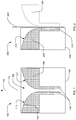
- FIGs. 3-6 show an exemplary planar transmission line to waveguide transition.
- a half-notch antenna 300 which is only partially visible, may be used as a transition between a microstrip line 330 and a waveguide 350.
- the half-notch antenna 300 may be inserted into an open end of the waveguide 350.
- the walls of the waveguide 350 may act as a ground plane to reflect a virtual image (not shown) of the half notch antenna 300.
- the half notch antenna 300 and the virtual image may effectively constitute a notch antenna as previously described.
- the waveguide 350 is shown with a rectangular cross section, but the waveguide 350 may be rectangular, square, circular, or may have some other geometric or arbitrary cross-sectional shape.
- the cross sections shape may vary along waveguide.
- the microstrip line 330 may be formed on a dielectric substrate 332.
- the dielectric substrate 332 may be coupled to a ground plane slab 340.
- the dielectric substrate 332 may be, for example, bonded to the ground plane slab 340.
- the ground plane slab 340 may serve as a heat sink to spread or remove heat generated by electronic components (not shown) mounted on the dielectric substrate 332.
- the ground plane slab 340 may be formed of, for example, copper, aluminum, or another electrically and thermally conductive material.
- the ground plane slab 340 may be electrically connected to the waveguide 350.
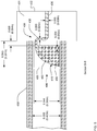
- FIGs. 4 , 5 , and 6 are cross-sectional views of specific exemplary half-notch antenna 400 designed to couple a 95 GHz signal from a microstrip line to a WG10 rectangular waveguide having internal dimensions of 0.05 inch by 0.10 inch. Dimensions in FIGs. 4 , 5 , and 6 are provided in inches for the specific example and as multiples of the signal wavelength, in parenthesis. The half notch antenna 400 of FIGs. 4 , 5 , and 6 may be scaled for other wavelengths and other waveguide dimensions.
- a microstrip to waveguide transition such as the half notch antenna 400, may be designed and simulated using a software tool adapted to solve three-dimensional electromagnetic field problems.
- the software tool may be a commercially available electromagnetic field analysis tool such as CST Microwave StudioTM, Agilent's MomentumTM tool, or Ansoft's HFSSTM tool.
- the electromagnetic field analysis tool may be a proprietary tool using any known mathematical method, such as finite difference time domain analysis, finite element method, boundary element method, method of moments, or other methods for solving electromagnetic field problems.
- the software tool may include a capability to iteratively optimize a design to meet predetermined performance targets. The example of FIGs. 4 , 5 , and 6 may provide a starting point for the design of planer transmission line to waveguide transitions for other wavelengths and/or other waveguide shapes.
- FIG. 4 shows a cross-sectional view of the exemplary microstrip to waveguide transition at a section plane A-A defined in FIG. 3 .
- a microstrip line 430 may be formed on a first surface 431 of a dielectric substrate 432.
- a ground plane 434 may be formed on at least a portion of a second surface 433 of the dielectric substrate 432.
- the dielectric substrate 432 may be coupled to, and supported by, a ground plane slab 440 in electrical contact with the ground plane 434.
- the half-notch antenna 400 may be formed on an extended portion of the dielectric substrate 432 that extends past an edge 442 of the ground plane slab 440 into an open end of a waveguide 450.
- the ground plane slab 440 may be in electrical contact with the waveguide 450.
- the ground plane slab 440 may block a portion 454 of the open end of the waveguide 450.
- Another portion 452 of the open end of the waveguide 450 may be unblocked.
- the unblocked portion 452 may be cut off (may not allow energy to exit the waveguide) at a frequency of operation of the microstrip to waveguide transition 400 if the height of the open portion 452 (0.030 inches in this example) is less than one-half of the wavelength at the frequency of operation.
- the height of the unblocked portion 452 may be a degree of design freedom that may be adjusted as part of optimizing the design of the microstrip to waveguide transition.
- the ground plane slab may block a central portion (not shown in FIG. 4 ) of the open end of the waveguide, leaving upper and lower unblocked portions (not shown).
- the open end of the waveguide may still be cutoff if the conductivity of the ground plane slab is sufficient to effectively short the open end of the waveguide.
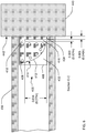
- FIG. 5 shows a cross-sectional view of the exemplary microstrip to waveguide transition at a section plane B-B defined in FIG. 4 .
- FIG. 5 shows a cross-section of the waveguide 450 and a top view of the first surface 431 of the dielectric substrate 432.
- the microstrip line 430 may be formed on the first surface 431.
- a half-notch antenna 400 may be formed on an extended portion 406 of the dielectric substrate 432.
- the half-notch antenna may include a first tapered conductor 402 formed on the first surface 431 of the extended portion 406.
- the tapered conductor 402 may be connected to the microstrip line 430 through an impedance transformer 436, which may be implemented, for example, by a narrow (compared to the microstrip line 430) conductor 438 formed on the first surface 431.
- the impedance transformer 436 may be implemented by other conductor configurations formed on the first surface 431.
- the impedance transformer 436 may match the impedance of the microstrip line 430 to the half notch antenna 400.
- An edge 410 of the tapered conductor 402 may be linear or curved. When the edge 410 is curved, as shown in FIG. 5 , the tapered conductor 402 may be considered to form one-half of a Vivaldi antenna.
- the edge 410 may follow a circular, elliptical, parabolic, or other curved shape.
- the edge 410 may follow a series of linear segments or steps that approximate a curved shape.
- the half-notch antenna 400 may include a second conductor (not visible) formed on a second surface of the extended portion 406.
- the tapered conductor 402 may be connected to the second conductor through one or more conductive vias 408.
- the conductive vias 408 may be, for example, plated through holes.
- FIG. 6 shows a cross-sectional view of the exemplary microstrip to waveguide transition at a section plane C-C defined in FIG. 4 .
- FIG. 5 shows a cross-section of the waveguide 450 and the ground plane slab 440, and a plan view of the second surface 433 of the extended portion 406 the dielectric substrate.
- the half-notch antenna 400 may include a second tapered conductor 412 formed on the second surface 433 of the extended portion 406.
- An edge 414 of the second tapered conductor 412 may have essentially the same contour as the edge 410 of the first conductor 402 of FIG. 5 .
- the second tapered conductor 412 may be connected to the first tapered conductor 402 through plurality of conductive vias 408.
- a ground plane 434 may be formed on the second surface 433 of the dielectric substrate.
- the ground plane 434 may extend past the edge 442 of the ground plane slab 440 onto the extended portion 406 of the dielectric substrate.
- the second tapered conductor 412 may be separated from the ground plane 434 by a gap 416 extending over a portion of a width of the second tapered conductor, and may be connected to the ground plane 434 by a conductor 418.
- FIG. 7 shows a graph 700 of the expected W-band performance of a microstrip to waveguide transition, derived from simulation of the microstrip to waveguide transition 400 as shown in FIGs. 4 , 5 , and 6 .
- the dashed line 702 and the solid line 704 represent the return loss for signals coupled from the microstrip to the waveguide, and from the waveguide to the microstrip, respectively.
- the return loss is more than 10 dB over a frequency band from about 81 GHz to more than 110 GHz.
- the solid line 706 represents the insertion loss for signals coupled from the microstrip to the waveguide.
- the insertion loss is less than 1 db over the 81 GHZ to 110 GHz frequency range.
- the insertion loss is nearly zero from 90 GHz to 100 GHz.
Landscapes
- Waveguide Aerials (AREA)
Claims (9)
- Module de circuit comportant une transition destinée au couplage d'un signal hyperfréquence dans un guide d'ondes creux (450), le module de circuit comprenant :une plaque conductrice faisant plan de masse (440) ayant un bord (442) ;un substrat diélectrique (432) couplé à la plaque conductrice faisant plan de masse (440), le substrat diélectrique comportant une partie prolongée (406) s'étendant au-delà du bord (442) de la plaque faisant plan de masse (440) et configurée pour être insérée à travers une extrémité ouverte du guide d'ondes creux (450) et à l'intérieur d'un passage creux du guide d'ondes creux (450) ;dans lequel la transition comprend :une ligne de transmission (430) formée sur le substrat diélectrique (432) ; etune antenne à demi-encoche (400) formée sur la partie prolongée (406) du substrat diélectrique (432) et couplée à la ligne de transmission (430) ; etdans lequel l'antenne à demi-encoche (400) comprend :un premier conducteur effilé (402) formé sur une première surface (431) du substrat diélectrique (432) et changeant progressivement de largeur de plus large à plus étroit le long d'une direction de propagation du signal hyperfréquence ;un deuxième conducteur effilé (412) formé sur une deuxième surface (433) du substrat diélectrique (432) et changeant progressivement de largeur de plus large à plus étroit le long de la direction de propagation du signal hyperfréquence, la deuxième surface (433) du substrat diélectrique (432) étant sur un côté sensiblement opposé à la première surface (431) ; etau moins un trou d'interconnexion conducteur (408) reliant le premier conducteur effilé (402) et le deuxième conducteur effilé (412).
- Module de la revendication 1, dans lequel le premier conducteur effilé (402) forme la moitié d'une antenne Vivaldi.
- Module de la revendication 1, dans lequel le deuxième conducteur effilé (412) est relié à un plan de masse (434) formé sur la deuxième surface (433) du substrat diélectrique (432) par un connecteur (418).
- Module de la revendication 1, dans lequel la ligne de transmission (430) est choisie dans le groupe constitué par une ligne microruban, une ligne ruban, une ligne à fente, et un guide d'ondes coplanaire.
- Module de la revendication 4, dans lequel :la ligne de transmission (430) est une ligne microruban formée sur la première surface (431) du substrat diélectrique (432), etle premier conducteur effilé (402) est couplé à la ligne microruban (430) par un transformateur d'impédance (436) formé sur la première surface (431) du substrat diélectrique (432).
- Système de transmission de signal hyperfréquence, comprenant :un guide d'ondes conducteur allongé (450) ayant une extrémité ouverte et un passage creux étant s'étendant depuis l'extrémité ouverte, le passage creux adapté pour guider une onde électromagnétique ; etle module de circuit d'une quelconque revendication précédente, disposé à proximité de l'extrémité ouverte du guide d'ondes, avec la partie prolongée (406) s'étendant au-delà du bord (442) de la plaque faisant plan de masse (440) à travers l'extrémité ouverte et à l'intérieur du passage creux du guide d'ondes.
- Système de transmission de signal hyperfréquence de la revendication 6, dans lequel le passage creux a une forme en coupe transversale choisie parmi rectangulaire, carrée, et circulaire.
- Système de transmission de signal hyperfréquence de la revendication 6, dans lequel la plaque faisant plan de masse (440) bloque une partie suffisante (454) de l'extrémité ouverte du guide d'ondes pour empêcher l'énergie de sortir par l'extrémité ouverte du guide d'ondes.
- Système de transmission de signal hyperfréquence de la revendication 8, dans lequel une hauteur d'une partie non bloquée (452) de l'extrémité ouverte du guide d'ondes est inférieure à la moitié d'une longueur d'onde du signal hyperfréquence.
Applications Claiming Priority (2)
| Application Number | Priority Date | Filing Date | Title |
|---|---|---|---|
| US12/612,591 US8305280B2 (en) | 2009-11-04 | 2009-11-04 | Low loss broadband planar transmission line to waveguide transition |
| PCT/US2010/047576 WO2011056287A1 (fr) | 2009-11-04 | 2010-09-01 | Ligne de transmission plane large bande a faibles pertes vers une transition de guide d'onde |
Publications (3)
| Publication Number | Publication Date |
|---|---|
| EP2497146A1 EP2497146A1 (fr) | 2012-09-12 |
| EP2497146B1 true EP2497146B1 (fr) | 2018-11-14 |
| EP2497146B8 EP2497146B8 (fr) | 2019-01-09 |
Family
ID=43086194
Family Applications (1)
| Application Number | Title | Priority Date | Filing Date |
|---|---|---|---|
| EP10754620.2A Active EP2497146B8 (fr) | 2009-11-04 | 2010-09-01 | Ligne de transmission plane large bande a faibles pertes vers une transition de guide d'onde |
Country Status (4)
| Country | Link |
|---|---|
| US (1) | US8305280B2 (fr) |
| EP (1) | EP2497146B8 (fr) |
| JP (1) | JP5362120B2 (fr) |
| WO (1) | WO2011056287A1 (fr) |
Cited By (1)
| Publication number | Priority date | Publication date | Assignee | Title |
|---|---|---|---|---|
| EP4012834B1 (fr) * | 2020-12-10 | 2024-02-21 | Thales | Source d'antenne pour une antenne réseau à rayonnement direct, panneau rayonnant et antenne comprenant plusieurs sources d'antenne |
Families Citing this family (32)
| Publication number | Priority date | Publication date | Assignee | Title |
|---|---|---|---|---|
| GB201113131D0 (en) * | 2011-07-29 | 2011-09-14 | Bae Systems Plc | Radio frequency communication |
| KR101343718B1 (ko) * | 2011-08-09 | 2013-12-20 | 주식회사 만도 | 바룬을 포함하는 레이더 시스템 |
| US9627777B2 (en) | 2011-08-10 | 2017-04-18 | Lawrence Livermore National Security, Llc | Broad band antennas and feed methods |
| US8552813B2 (en) | 2011-11-23 | 2013-10-08 | Raytheon Company | High frequency, high bandwidth, low loss microstrip to waveguide transition |
| JP5628245B2 (ja) * | 2012-07-27 | 2014-11-19 | 日本電信電話株式会社 | ガイド付き平面アンテナ |
| JP6039472B2 (ja) * | 2013-03-15 | 2016-12-07 | 日東電工株式会社 | アンテナモジュールおよびその製造方法 |
| FR3010835B1 (fr) | 2013-09-19 | 2015-09-11 | Inst Mines Telecom Telecom Bretagne | Dispositif de jonction entre une ligne de transmission imprimee et un guide d'ondes dielectrique |
| RU2584502C2 (ru) * | 2013-12-30 | 2016-05-20 | Федеральное государственное бюджетное образовательное учреждение высшего профессионального образования "Томский государственный университет систем управления и радиоэлектроники" | Микрополосковая линия со стабильной задержкой |
| JP6216267B2 (ja) * | 2014-03-10 | 2017-10-18 | 日本ピラー工業株式会社 | アンテナ用ユニット |
| US9917372B2 (en) | 2014-06-13 | 2018-03-13 | Nxp Usa, Inc. | Integrated circuit package with radio frequency coupling arrangement |
| US10103447B2 (en) | 2014-06-13 | 2018-10-16 | Nxp Usa, Inc. | Integrated circuit package with radio frequency coupling structure |
| US9620841B2 (en) | 2014-06-13 | 2017-04-11 | Nxp Usa, Inc. | Radio frequency coupling structure |
| US10225925B2 (en) | 2014-08-29 | 2019-03-05 | Nxp Usa, Inc. | Radio frequency coupling and transition structure |
| US9887449B2 (en) | 2014-08-29 | 2018-02-06 | Nxp Usa, Inc. | Radio frequency coupling structure and a method of manufacturing thereof |
| US9444135B2 (en) | 2014-09-19 | 2016-09-13 | Freescale Semiconductor, Inc. | Integrated circuit package |
| GB2531082B (en) * | 2014-10-10 | 2018-04-04 | Kathrein Werke Kg | Half-ridge horn antenna array arrangement |
| US10615499B2 (en) | 2015-01-14 | 2020-04-07 | Skywave Mobile Communications Inc. | Dual role antenna assembly |
| SE541830C2 (en) * | 2015-02-19 | 2019-12-27 | Trxmems Ab | Mems based waveguide chip |
| US9929775B2 (en) * | 2015-03-25 | 2018-03-27 | Intel Corporation | Techniques for device-to-device communications |
| RU2607252C1 (ru) * | 2015-07-16 | 2017-01-10 | Федеральное государственное бюджетное образовательное учреждение высшего профессионального образования "Томский государственный университет систем управления и радиоэлектроники" (ТУСУР) | Меандровая микрополосковая линия задержки, защищающая от сверхкоротких импульсов |
| US9692135B1 (en) | 2015-12-10 | 2017-06-27 | Semiconductor Components Industries, Llc | Direct transition from a waveguide to a buried chip |
| WO2018057002A1 (fr) | 2016-09-23 | 2018-03-29 | Intel Corporation | Systèmes et procédés de couplage de guides d'ondes |
| US10566672B2 (en) | 2016-09-27 | 2020-02-18 | Intel Corporation | Waveguide connector with tapered slot launcher |
| US10256521B2 (en) | 2016-09-29 | 2019-04-09 | Intel Corporation | Waveguide connector with slot launcher |
| US11394094B2 (en) | 2016-09-30 | 2022-07-19 | Intel Corporation | Waveguide connector having a curved array of waveguides configured to connect a package to excitation elements |
| RU2691844C1 (ru) * | 2018-06-18 | 2019-06-18 | Федеральное государственное бюджетное образовательное учреждение высшего образования "Томский государственный университет систем управления и радиоэлектроники" | Усовершенствованная меандровая микрополосковая линия задержки, защищающая от электростатического разряда |
| CN111193087A (zh) * | 2018-11-14 | 2020-05-22 | 日本电产株式会社 | 波导装置以及信号发生装置 |
| EP4010942A1 (fr) * | 2019-09-27 | 2022-06-15 | Sony Group Corporation | Antenne destinée à être utilisée dans un terminal de communication radio |
| CN113937450B (zh) * | 2020-06-29 | 2022-12-27 | 华为技术有限公司 | 耦合器、收发模块及通信系统 |
| JP2024054432A (ja) * | 2021-02-01 | 2024-04-17 | 国立大学法人東京工業大学 | アレーアンテナ |
| CN114284676B (zh) * | 2021-12-24 | 2022-07-29 | 电子科技大学 | 一种基于v型天线的波导-微带过渡结构 |
| CN118352779A (zh) * | 2024-04-29 | 2024-07-16 | 深圳市信维通信股份有限公司 | 一种波导天线、雷达及汽车 |
Citations (1)
| Publication number | Priority date | Publication date | Assignee | Title |
|---|---|---|---|---|
| JPH04271501A (ja) * | 1991-02-26 | 1992-09-28 | Toshiba Corp | 導波管−マイクロストリップ線路変換器 |
Family Cites Families (22)
| Publication number | Priority date | Publication date | Assignee | Title |
|---|---|---|---|---|
| US3969691A (en) * | 1975-06-11 | 1976-07-13 | The United States Of America As Represented By The Secretary Of The Navy | Millimeter waveguide to microstrip transition |
| US4260964A (en) * | 1979-05-07 | 1981-04-07 | The United States Of America As Represented By The Secretary Of The Navy | Printed circuit waveguide to microstrip transition |
| DE3217945A1 (de) * | 1982-05-13 | 1984-02-02 | ANT Nachrichtentechnik GmbH, 7150 Backnang | Uebergang von einem hohlleiter auf eine mikrostreifenleitung |
| US4500887A (en) * | 1982-09-30 | 1985-02-19 | General Electric Company | Microstrip notch antenna |
| US4672384A (en) * | 1984-12-31 | 1987-06-09 | Raytheon Company | Circularly polarized radio frequency antenna |
| US4651115A (en) * | 1985-01-31 | 1987-03-17 | Rca Corporation | Waveguide-to-microstrip transition |
| US4782346A (en) * | 1986-03-11 | 1988-11-01 | General Electric Company | Finline antennas |
| US5202648A (en) * | 1991-12-09 | 1993-04-13 | The Boeing Company | Hermetic waveguide-to-microstrip transition module |
| US5600286A (en) * | 1994-09-29 | 1997-02-04 | Hughes Electronics | End-on transmission line-to-waveguide transition |
| JP2661568B2 (ja) | 1994-11-14 | 1997-10-08 | 日本電気株式会社 | 導波管・平面線路変換器 |
| US6100853A (en) * | 1997-09-10 | 2000-08-08 | Hughes Electronics Corporation | Receiver/transmitter system including a planar waveguide-to-stripline adapter |
| US6002305A (en) | 1997-09-25 | 1999-12-14 | Endgate Corporation | Transition between circuit transmission line and microwave waveguide |
| DE19805911A1 (de) * | 1998-02-13 | 1999-08-19 | Cit Alcatel | Übergang von einer Mikrostripleitung zu einem Hohlleiter sowie Verwendung eines solchen Übergangs |
| US6043785A (en) * | 1998-11-30 | 2000-03-28 | Radio Frequency Systems, Inc. | Broadband fixed-radius slot antenna arrangement |
| US6127901A (en) * | 1999-05-27 | 2000-10-03 | Hrl Laboratories, Llc | Method and apparatus for coupling a microstrip transmission line to a waveguide transmission line for microwave or millimeter-wave frequency range transmission |
| JP3672241B2 (ja) | 2001-01-11 | 2005-07-20 | 三菱電機株式会社 | 導波管/マイクロストリップ線路変換器およびこれを用いた高周波パッケージ |
| GB0108696D0 (en) * | 2001-04-05 | 2001-05-30 | Koninkl Philips Electronics Nv | A transition from microstrip to waveguide |
| GB2379088B (en) * | 2001-08-24 | 2005-06-01 | Roke Manor Research | Improvements in antennas |
| JP2003078310A (ja) * | 2001-09-04 | 2003-03-14 | Murata Mfg Co Ltd | 高周波用線路変換器、部品、モジュールおよび通信装置 |
| FR2849720B1 (fr) * | 2003-01-03 | 2005-04-15 | Thomson Licensing Sa | Transition entre un guide d'onde rectangulaire et une ligne microruban |
| US7193575B2 (en) * | 2003-04-25 | 2007-03-20 | Qualcomm Incorporated | Wideband antenna with transmission line elbow |
| US6967624B1 (en) * | 2004-04-23 | 2005-11-22 | Lockheed Martin Corporation | Wideband antenna element and array thereof |
-
2009
- 2009-11-04 US US12/612,591 patent/US8305280B2/en active Active
-
2010
- 2010-09-01 EP EP10754620.2A patent/EP2497146B8/fr active Active
- 2010-09-01 WO PCT/US2010/047576 patent/WO2011056287A1/fr not_active Ceased
- 2010-09-01 JP JP2012536807A patent/JP5362120B2/ja active Active
Patent Citations (2)
| Publication number | Priority date | Publication date | Assignee | Title |
|---|---|---|---|---|
| JPH04271501A (ja) * | 1991-02-26 | 1992-09-28 | Toshiba Corp | 導波管−マイクロストリップ線路変換器 |
| JP3169972B2 (ja) * | 1991-02-26 | 2001-05-28 | 株式会社東芝 | 導波管−マイクロストリップ線路変換器 |
Cited By (1)
| Publication number | Priority date | Publication date | Assignee | Title |
|---|---|---|---|---|
| EP4012834B1 (fr) * | 2020-12-10 | 2024-02-21 | Thales | Source d'antenne pour une antenne réseau à rayonnement direct, panneau rayonnant et antenne comprenant plusieurs sources d'antenne |
Also Published As
| Publication number | Publication date |
|---|---|
| US8305280B2 (en) | 2012-11-06 |
| EP2497146B8 (fr) | 2019-01-09 |
| WO2011056287A1 (fr) | 2011-05-12 |
| JP5362120B2 (ja) | 2013-12-11 |
| EP2497146A1 (fr) | 2012-09-12 |
| US20110102284A1 (en) | 2011-05-05 |
| JP2013510466A (ja) | 2013-03-21 |
Similar Documents
| Publication | Publication Date | Title |
|---|---|---|
| EP2497146B1 (fr) | Ligne de transmission plane large bande a faibles pertes vers une transition de guide d'onde | |
| EP3460908B1 (fr) | Antenne de réseau en phase | |
| Djerafi et al. | Super-compact substrate integrated waveguide cruciform directional coupler | |
| EP2783419B1 (fr) | Microruban à haute fréquence, à large bande passante et à faible perte sur transition de guide d'ondes | |
| US20110037530A1 (en) | Stripline to waveguide perpendicular transition | |
| KR101120043B1 (ko) | 마이크로스트립 선로와 서스펜디드 스트립선로간 전이구조 및 그 응용 모듈 | |
| JP2005045815A (ja) | ミリ波信号変換デバイス | |
| CN109616764B (zh) | 基片集成间隙波导圆极化天线 | |
| EP2315304B1 (fr) | Circuit de terminaison de bandelette doté de résonateurs | |
| US7002433B2 (en) | Microwave coupler | |
| US20220059916A1 (en) | Transmission line and electronic apparatus | |
| KR101182425B1 (ko) | 스터브가 있는 슬롯 안테나 | |
| CN116031601B (zh) | 一种平面传输线至矩形波导的转换结构 | |
| Taringou et al. | New substrate-integrated to coplanar waveguide transition | |
| Yuasa et al. | A millimeter wave wideband differential line to waveguide transition using short ended slot line | |
| Logan et al. | On the design of 6∶ 1 mm-wave PUMA arrays | |
| KR100986190B1 (ko) | 동축커넥터 변환 구조체 | |
| Taringou et al. | New interface design from substrate-integrated to regular coplanar waveguide | |
| Liu et al. | A dual-board substrate integrated waveguide for large phase delay application | |
| CN120089923A (zh) | 共面波导-矩形波导水平转换馈电结构和波导缝隙天线 | |
| KR20220055435A (ko) | 금속선 모드 변환기 | |
| US20080111654A1 (en) | Transmission Arrangement | |
| Nahid et al. | An analysis of a tetrahedral-slot and substrate integrated waveguide fed microstrip patch antenna | |
| Labay et al. | Substrate-integrated waveguide-to-microstrip couplers for integrated-circuit antenna applications |
Legal Events
| Date | Code | Title | Description |
|---|---|---|---|
| PUAI | Public reference made under article 153(3) epc to a published international application that has entered the european phase |
Free format text: ORIGINAL CODE: 0009012 |
|
| 17P | Request for examination filed |
Effective date: 20120601 |
|
| AK | Designated contracting states |
Kind code of ref document: A1 Designated state(s): AL AT BE BG CH CY CZ DE DK EE ES FI FR GB GR HR HU IE IS IT LI LT LU LV MC MK MT NL NO PL PT RO SE SI SK SM TR |
|
| DAX | Request for extension of the european patent (deleted) | ||
| 17Q | First examination report despatched |
Effective date: 20140729 |
|
| GRAP | Despatch of communication of intention to grant a patent |
Free format text: ORIGINAL CODE: EPIDOSNIGR1 |
|
| STAA | Information on the status of an ep patent application or granted ep patent |
Free format text: STATUS: GRANT OF PATENT IS INTENDED |
|
| INTG | Intention to grant announced |
Effective date: 20180718 |
|
| GRAS | Grant fee paid |
Free format text: ORIGINAL CODE: EPIDOSNIGR3 |
|
| GRAA | (expected) grant |
Free format text: ORIGINAL CODE: 0009210 |
|
| STAA | Information on the status of an ep patent application or granted ep patent |
Free format text: STATUS: THE PATENT HAS BEEN GRANTED |
|
| AK | Designated contracting states |
Kind code of ref document: B1 Designated state(s): AL AT BE BG CH CY CZ DE DK EE ES FI FR GB GR HR HU IE IS IT LI LT LU LV MC MK MT NL NO PL PT RO SE SI SK SM TR |
|
| REG | Reference to a national code |
Ref country code: GB Ref legal event code: FG4D |
|
| REG | Reference to a national code |
Ref country code: CH Ref legal event code: EP Ref country code: AT Ref legal event code: REF Ref document number: 1065919 Country of ref document: AT Kind code of ref document: T Effective date: 20181115 |
|
| REG | Reference to a national code |
Ref country code: DE Ref legal event code: R096 Ref document number: 602010055098 Country of ref document: DE |
|
| REG | Reference to a national code |
Ref country code: IE Ref legal event code: FG4D |
|
| REG | Reference to a national code |
Ref country code: CH Ref legal event code: PK Free format text: BERICHTIGUNG B8 |
|
| RAP2 | Party data changed (patent owner data changed or rights of a patent transferred) |
Owner name: RAYTHEON COMPANY |
|
| REG | Reference to a national code |
Ref country code: DE Ref legal event code: R081 Ref document number: 602010055098 Country of ref document: DE Owner name: RAYTHEON COMPANY, WALTHAM, US Free format text: FORMER OWNERS: BROWN, ANDREW K., TUCSON, AZ, US; GRITTERS, DARIN M., TUCSON, AZ, US; RAYTHEON CO., WALTHAM, MASS., US |
|
| REG | Reference to a national code |
Ref country code: GB Ref legal event code: 732E Free format text: REGISTERED BETWEEN 20190222 AND 20190227 Ref country code: NL Ref legal event code: MP Effective date: 20181114 |
|
| REG | Reference to a national code |
Ref country code: LT Ref legal event code: MG4D |
|
| REG | Reference to a national code |
Ref country code: AT Ref legal event code: MK05 Ref document number: 1065919 Country of ref document: AT Kind code of ref document: T Effective date: 20181114 |
|
| PG25 | Lapsed in a contracting state [announced via postgrant information from national office to epo] |
Ref country code: FI Free format text: LAPSE BECAUSE OF FAILURE TO SUBMIT A TRANSLATION OF THE DESCRIPTION OR TO PAY THE FEE WITHIN THE PRESCRIBED TIME-LIMIT Effective date: 20181114 Ref country code: AT Free format text: LAPSE BECAUSE OF FAILURE TO SUBMIT A TRANSLATION OF THE DESCRIPTION OR TO PAY THE FEE WITHIN THE PRESCRIBED TIME-LIMIT Effective date: 20181114 Ref country code: HR Free format text: LAPSE BECAUSE OF FAILURE TO SUBMIT A TRANSLATION OF THE DESCRIPTION OR TO PAY THE FEE WITHIN THE PRESCRIBED TIME-LIMIT Effective date: 20181114 Ref country code: LV Free format text: LAPSE BECAUSE OF FAILURE TO SUBMIT A TRANSLATION OF THE DESCRIPTION OR TO PAY THE FEE WITHIN THE PRESCRIBED TIME-LIMIT Effective date: 20181114 Ref country code: NO Free format text: LAPSE BECAUSE OF FAILURE TO SUBMIT A TRANSLATION OF THE DESCRIPTION OR TO PAY THE FEE WITHIN THE PRESCRIBED TIME-LIMIT Effective date: 20190214 Ref country code: IS Free format text: LAPSE BECAUSE OF FAILURE TO SUBMIT A TRANSLATION OF THE DESCRIPTION OR TO PAY THE FEE WITHIN THE PRESCRIBED TIME-LIMIT Effective date: 20190314 Ref country code: ES Free format text: LAPSE BECAUSE OF FAILURE TO SUBMIT A TRANSLATION OF THE DESCRIPTION OR TO PAY THE FEE WITHIN THE PRESCRIBED TIME-LIMIT Effective date: 20181114 Ref country code: LT Free format text: LAPSE BECAUSE OF FAILURE TO SUBMIT A TRANSLATION OF THE DESCRIPTION OR TO PAY THE FEE WITHIN THE PRESCRIBED TIME-LIMIT Effective date: 20181114 Ref country code: BG Free format text: LAPSE BECAUSE OF FAILURE TO SUBMIT A TRANSLATION OF THE DESCRIPTION OR TO PAY THE FEE WITHIN THE PRESCRIBED TIME-LIMIT Effective date: 20190214 |
|
| PG25 | Lapsed in a contracting state [announced via postgrant information from national office to epo] |
Ref country code: AL Free format text: LAPSE BECAUSE OF FAILURE TO SUBMIT A TRANSLATION OF THE DESCRIPTION OR TO PAY THE FEE WITHIN THE PRESCRIBED TIME-LIMIT Effective date: 20181114 Ref country code: PT Free format text: LAPSE BECAUSE OF FAILURE TO SUBMIT A TRANSLATION OF THE DESCRIPTION OR TO PAY THE FEE WITHIN THE PRESCRIBED TIME-LIMIT Effective date: 20190314 Ref country code: SE Free format text: LAPSE BECAUSE OF FAILURE TO SUBMIT A TRANSLATION OF THE DESCRIPTION OR TO PAY THE FEE WITHIN THE PRESCRIBED TIME-LIMIT Effective date: 20181114 Ref country code: NL Free format text: LAPSE BECAUSE OF FAILURE TO SUBMIT A TRANSLATION OF THE DESCRIPTION OR TO PAY THE FEE WITHIN THE PRESCRIBED TIME-LIMIT Effective date: 20181114 Ref country code: GR Free format text: LAPSE BECAUSE OF FAILURE TO SUBMIT A TRANSLATION OF THE DESCRIPTION OR TO PAY THE FEE WITHIN THE PRESCRIBED TIME-LIMIT Effective date: 20190215 |
|
| PG25 | Lapsed in a contracting state [announced via postgrant information from national office to epo] |
Ref country code: CZ Free format text: LAPSE BECAUSE OF FAILURE TO SUBMIT A TRANSLATION OF THE DESCRIPTION OR TO PAY THE FEE WITHIN THE PRESCRIBED TIME-LIMIT Effective date: 20181114 Ref country code: PL Free format text: LAPSE BECAUSE OF FAILURE TO SUBMIT A TRANSLATION OF THE DESCRIPTION OR TO PAY THE FEE WITHIN THE PRESCRIBED TIME-LIMIT Effective date: 20181114 Ref country code: IT Free format text: LAPSE BECAUSE OF FAILURE TO SUBMIT A TRANSLATION OF THE DESCRIPTION OR TO PAY THE FEE WITHIN THE PRESCRIBED TIME-LIMIT Effective date: 20181114 Ref country code: DK Free format text: LAPSE BECAUSE OF FAILURE TO SUBMIT A TRANSLATION OF THE DESCRIPTION OR TO PAY THE FEE WITHIN THE PRESCRIBED TIME-LIMIT Effective date: 20181114 |
|
| REG | Reference to a national code |
Ref country code: DE Ref legal event code: R097 Ref document number: 602010055098 Country of ref document: DE |
|
| PG25 | Lapsed in a contracting state [announced via postgrant information from national office to epo] |
Ref country code: EE Free format text: LAPSE BECAUSE OF FAILURE TO SUBMIT A TRANSLATION OF THE DESCRIPTION OR TO PAY THE FEE WITHIN THE PRESCRIBED TIME-LIMIT Effective date: 20181114 Ref country code: SM Free format text: LAPSE BECAUSE OF FAILURE TO SUBMIT A TRANSLATION OF THE DESCRIPTION OR TO PAY THE FEE WITHIN THE PRESCRIBED TIME-LIMIT Effective date: 20181114 Ref country code: SK Free format text: LAPSE BECAUSE OF FAILURE TO SUBMIT A TRANSLATION OF THE DESCRIPTION OR TO PAY THE FEE WITHIN THE PRESCRIBED TIME-LIMIT Effective date: 20181114 Ref country code: RO Free format text: LAPSE BECAUSE OF FAILURE TO SUBMIT A TRANSLATION OF THE DESCRIPTION OR TO PAY THE FEE WITHIN THE PRESCRIBED TIME-LIMIT Effective date: 20181114 |
|
| PLBE | No opposition filed within time limit |
Free format text: ORIGINAL CODE: 0009261 |
|
| STAA | Information on the status of an ep patent application or granted ep patent |
Free format text: STATUS: NO OPPOSITION FILED WITHIN TIME LIMIT |
|
| 26N | No opposition filed |
Effective date: 20190815 |
|
| PG25 | Lapsed in a contracting state [announced via postgrant information from national office to epo] |
Ref country code: SI Free format text: LAPSE BECAUSE OF FAILURE TO SUBMIT A TRANSLATION OF THE DESCRIPTION OR TO PAY THE FEE WITHIN THE PRESCRIBED TIME-LIMIT Effective date: 20181114 |
|
| PG25 | Lapsed in a contracting state [announced via postgrant information from national office to epo] |
Ref country code: TR Free format text: LAPSE BECAUSE OF FAILURE TO SUBMIT A TRANSLATION OF THE DESCRIPTION OR TO PAY THE FEE WITHIN THE PRESCRIBED TIME-LIMIT Effective date: 20181114 |
|
| PG25 | Lapsed in a contracting state [announced via postgrant information from national office to epo] |
Ref country code: MC Free format text: LAPSE BECAUSE OF FAILURE TO SUBMIT A TRANSLATION OF THE DESCRIPTION OR TO PAY THE FEE WITHIN THE PRESCRIBED TIME-LIMIT Effective date: 20181114 |
|
| REG | Reference to a national code |
Ref country code: CH Ref legal event code: PL |
|
| PG25 | Lapsed in a contracting state [announced via postgrant information from national office to epo] |
Ref country code: LU Free format text: LAPSE BECAUSE OF NON-PAYMENT OF DUE FEES Effective date: 20190901 Ref country code: IE Free format text: LAPSE BECAUSE OF NON-PAYMENT OF DUE FEES Effective date: 20190901 Ref country code: LI Free format text: LAPSE BECAUSE OF NON-PAYMENT OF DUE FEES Effective date: 20190930 Ref country code: CH Free format text: LAPSE BECAUSE OF NON-PAYMENT OF DUE FEES Effective date: 20190930 |
|
| REG | Reference to a national code |
Ref country code: BE Ref legal event code: MM Effective date: 20190930 |
|
| PG25 | Lapsed in a contracting state [announced via postgrant information from national office to epo] |
Ref country code: BE Free format text: LAPSE BECAUSE OF NON-PAYMENT OF DUE FEES Effective date: 20190930 |
|
| PG25 | Lapsed in a contracting state [announced via postgrant information from national office to epo] |
Ref country code: CY Free format text: LAPSE BECAUSE OF FAILURE TO SUBMIT A TRANSLATION OF THE DESCRIPTION OR TO PAY THE FEE WITHIN THE PRESCRIBED TIME-LIMIT Effective date: 20181114 |
|
| PG25 | Lapsed in a contracting state [announced via postgrant information from national office to epo] |
Ref country code: MT Free format text: LAPSE BECAUSE OF FAILURE TO SUBMIT A TRANSLATION OF THE DESCRIPTION OR TO PAY THE FEE WITHIN THE PRESCRIBED TIME-LIMIT Effective date: 20181114 Ref country code: HU Free format text: LAPSE BECAUSE OF FAILURE TO SUBMIT A TRANSLATION OF THE DESCRIPTION OR TO PAY THE FEE WITHIN THE PRESCRIBED TIME-LIMIT; INVALID AB INITIO Effective date: 20100901 |
|
| PG25 | Lapsed in a contracting state [announced via postgrant information from national office to epo] |
Ref country code: MK Free format text: LAPSE BECAUSE OF FAILURE TO SUBMIT A TRANSLATION OF THE DESCRIPTION OR TO PAY THE FEE WITHIN THE PRESCRIBED TIME-LIMIT Effective date: 20181114 |
|
| P01 | Opt-out of the competence of the unified patent court (upc) registered |
Effective date: 20230530 |
|
| PGFP | Annual fee paid to national office [announced via postgrant information from national office to epo] |
Ref country code: DE Payment date: 20250820 Year of fee payment: 16 |
|
| PGFP | Annual fee paid to national office [announced via postgrant information from national office to epo] |
Ref country code: GB Payment date: 20250820 Year of fee payment: 16 |
|
| PGFP | Annual fee paid to national office [announced via postgrant information from national office to epo] |
Ref country code: FR Payment date: 20250820 Year of fee payment: 16 |